

Page 1
General Description
The MAX125/MAX126 are high-speed, multichannel,
14-bit data-acquisition systems (DAS) with simultaneous
track/holds (T/Hs). These devices contain a 14-bit, 3µs,
successive-approximation analog-to-digital converter
(ADC), a +2.5V reference, a buffered reference input,
and a bank of four simultaneous-sampling T/H amplifiers that preserve the relative phase information of the
sampled inputs. The MAX125/MAX126 have two multiplexed inputs for each T/H, allowing a total of eight
inputs. In addition, the converter is overvoltage tolerant
to ±17V; a fault condition on any channel will not harm
the IC. Available input ranges are ±5V (MAX125) and
±2.5V (MAX126).
An on-board sequencer converts one to four channels
per CONVST pulse. In the default mode, one T/H output
(CH1A) is converted. An interrupt signal (INT) is provided
after the last conversion is complete. Convert two,
three, or four channels by reprogramming the
MAX125/MAX126 through the bidirectional parallel
interface. Once programmed, the MAX125/MAX126
continue to convert the specified number of channels
per CONVST pulse until they are reprogrammed. The
channels are converted sequentially, beginning with
CH1. The INT signal always follows the end of the last
conversion in a conversion sequence. The ADC converts each assigned channel in 3µs and stores the
result in an internal 14x4 RAM. Upon completion of the
conversions, data can be accessed by applying successive pulses to the RD pin. Four successive reads
access four data words sequentially.
The parallel interface’s data-access and bus-release
timing specifications are compatible with most popular
digital signal processors and 16-bit/32-bit microprocessors, so the MAX125/MAX126 conversion results can
be accessed without resorting to wait states.
Applications
Multiphase Motor Control
Power-Grid Synchronization
Power-Factor Monitoring
Digital Signal Processing
Vibration and Waveform Analysis
Features
o Four Simultaneous-Sampling T/H Amplifiers with
Two Multiplexed Inputs (eight single-ended inputs
total)
o 3µs Conversion Time per Channel
o Throughput: 250ksps (1 channel)
142ksps (2 channels)
100ksps (3 channels)
76ksps (4 channels)
o Input Range: ±5V (MAX125)
±2.5V (MAX126)
o Fault-Protected Input Multiplexer (±17V)
o ±5V Supplies
o Internal +2.5V or External Reference Operation
o Programmable On-Board Sequencer
o High-Speed Parallel DSP Interface
MAX125/MAX126
2x4-Channel, Simultaneous-Sampling
14-Bit DAS
________________________________________________________________
Maxim Integrated Products
1
Ordering Information
19-1319; Rev 2; 6/07
For pricing delivery, and ordering information please contact Maxim Direct at 1-888-629-4642,
or visit Maxim’s website at www.maxim-ic.com.
Typical Operating Circuit appears at end of data sheet.
Pin Configuration appears at end of data sheet.
EVALUATION KIT
AVAILABLE
PART
TEMP RANGE
PIN-
INL
PKG
CODE
MAX125CCAX
A36-4
MAX125CEAX
A36-4
MAX126CCAX
A36-4
MAX126CEAX
A36-4
PACKAGE
0°C to +70°C 36 SSOP ±4
-40°C to +85°C 36 SSOP ±4
0°C to +70°C 36 SSOP ±4
-40°C to +85°C 36 SSOP ±4
(LSB)
Page 2
MAX125/MAX126
2x4-Channel, Simultaneous-Sampling
14-Bit DAS
2 _______________________________________________________________________________________
ABSOLUTE MAXIMUM RATINGS
ELECTRICAL CHARACTERISTICS
(AVDD= +5V ±5%, AVSS= -5V ±5%, DVDD= +5V ±5%, V
REFIN
= 2.5V, AGND = DGND = 0V, 4.7µF capacitor from REFOUT to
AGND, 0.1µF capacitor from REFIN to AGND, f
CLK
= 16MHz, external clock, 50% duty cycle, TA= T
MIN
to T
MAX
, unless otherwise
noted.)
Stresses beyond those listed under “Absolute Maximum Ratings” may cause permanent damage to the device. These are stress ratings only, and functional
operation of the device at these or any other conditions beyond those indicated in the operational sections of the specifications is not implied. Exposure to
absolute maximum rating conditions for extended periods may affect device reliability.
AVDDto AGND ...........................................................-0.3V to 6V
AV
SS
to AGND ............................................................0.3V to -6V
DVDDto DGND ...........................................................-0.3V to 6V
AGND to DGND .......................................................-0.3V to 0.3V
CH_ _ to AGND....................................................................±17V
REFIN, REFOUT to AGND ..........................................-0.3V to 6V
Digital Inputs/Outputs to DGND ..............-0.3V to (DV
DD
+ 0.3V)
Continuous Power Dissipation (T
A
= +70°C)
SSOP (derate 11.8mW/°C above +70°C) ....................941mW
Operating Temperature Ranges
MAX125CCAX/MAX126CCAX ............................0°C to +70°C
MAX125CEAX/MAX126CEAX..........................-40°C to +85°C
Storage Temperature Range .............................-65°C to +150°C
Lead Temperature (soldering, 10sec)................................300°C
DC ACCURACY (Note 1)
Resolution N All channels 14 Bits
Integral Nonlinearity INL (Note 2) ±2 ±4 LSB
Differential Nonlinearity DNL Guaranteed monotonic to 13 bits ±2 LSB
Bipolar Zero Error
Bipolar Zero-Error Match Between all channels 1.2 5 mV
Zero-Code Tempco ±5 ppm/°C
Gain Error
Gain-Error Match Between all channels 1.2 5 mV
Gain-Error Tempco ±5 ppm/°C
DYNAMIC PERFORMANCE (f
Signal-to-Noise Plus Distortion SINAD
Total Harmonic Distortion THD
Spurious-Free Dynamic Range SFDR
Channel-to-Channel Isolation
PARAMETER SYMBOL CONDITIONS MIN TYP MAX UNITS
= 16MHz, fIN = 10.06kHz (Notes 1, 3)
CLK
TA = +25°C ±5 ±15
T
A = TMIN
TA = +25°C ±5 ±10
T
A = TMIN
Single-channel mode,
channel 1A, 250ksps (Note 4)
Single-channel mode, channel 1A, 250ksps
(Notes 4, 5)
Single-channel mode, channel 1A, 250ksps
(Note 4)
Single-channel mode, channel 1A, 250ksps
(Note 6)
to T
MAX
to T
MAX
MAX125 72 75
MAX126 70 72
80 90 dB
-89 -80 dB
80 dB
±25
±15
mV
mV
dB
Page 3
µA
MAX125/MAX126
2x4-Channel, Simultaneous-Sampling
14-Bit DAS
_______________________________________________________________________________________ 3
ELECTRICAL CHARACTERISTICS (continued)
(AVDD= +5V ±5%, AVSS= -5V ±5%, DVDD= +5V ±5%, V
REFIN
= 2.5V, AGND = DGND = 0V, 4.7µF capacitor from REFOUT to
AGND, 0.1µF capacitor from REFIN to AGND, f
CLK
= 16MHz, external clock, 50% duty cycle, TA= T
MIN
to T
MAX
, unless otherwise
noted.)
CONDITIONS UNITSMIN TYP MAXSYMBOLPARAMETER
MAX125
V
±5
V
IN
Input Voltage Range
MAX125, VIN= ±5V
µA±667I
IN
Input Current
(Note 7) pF16C
IN
Input Capacitance
µs1t
ACQ
Acquisition Time
MHz8Small-Signal Bandwidth
MHz0.5Full-Power Bandwidth
mV/ms2Droop Rate
ns5Aperture Delay
ps
RMS
30Aperture Jitter
ps500Aperture-Delay Matching
TA= +25°C V2.475 2.500 2.525V
REFOUT
Output Voltage
0mA < I
LOAD
< 1mA %±1External Load Regulation
(Note 9) ppm/°C30REFOUT Tempco
µF0.1
External Capacitive
Bypass at REFIN
V2.50 ±10%Input Voltage Range
µF4.7 22
External Capacitive
Bypass at REFOUT
REFIN = 2.5V µA±10Input Current
(Note 10) kΩ10Input Resistance
(Note 7) pF10Input Capacitance
MHz0.1 16External Clock Frequency
V2.4V
IH
Input High Voltage
V0.8V
IL
Input Low Voltage
CONVST, RD, WR, CS, CLK
±1
(Note 7) pF15C
IN
Input Capacitance
A0–A3
µA
±10
I
IN
Input Current
MAX126 ±2.5
MAX126, VIN= ±2.5V
ANALOG INPUT
TRACK/HOLD
REFERENCE OUTPUT (Note 8)
REFERENCE INPUT
EXTERNAL CLOCK
DIGITAL INPUTS (CONVST, RD, WR, CS, CLK, A0–A3) (Note 1)
Page 4
MAX125/MAX126
2x4-Channel, Simultaneous-Sampling
14-Bit DAS
4 _______________________________________________________________________________________
CONDITIONS UNITSMIN TYP MAXSYMBOLPARAMETER
I
OUT
= 1mA V4V
OH
Output High Voltage
I
OUT
= -1.6mA V0.4V
OL
Output Low Voltage
D0–D13 µA±10Three-State Leakage Current
(Note 7) pF10
Three-State Output
Capacitance
V4.75 5 5.25AV
DD
Positive Supply Voltage
V-5.25 -5 -4.75AV
SS
Negative Supply Voltage
V4.75 5 5.25DV
DD
Digital Supply Voltage
mA17 25I(AVDD)Positive Supply Current
mA-17 -13I(AVSS)Negative Supply Current
mA3 5I(DVDD)Digital Supply Current
mA3Shutdown Positive Current
mA-1Shutdown Negative Current
mA3Shutdown Digital Current
(Note 11) LSB±1 ±2PSRR+Positive Supply Rejection
(Note 11) LSB±2PSRR-Negative Supply Rejection
(Note 12) mW165 250Power Dissipation
DIGITAL OUTPUTS (D0–D13, INT) (Note 1)
POWER REQUIREMENTS
ELECTRICAL CHARACTERISTICS (continued)
(AVDD= +5V ±5%, AVSS= -5V ±5%, DVDD= +5V ±5%, V
REFIN
= 2.5V, AGND = DGND = 0V, 4.7µF capacitor from REFOUT to
AGND, 0.1µF capacitor from REFIN to AGND, f
CLK
= 16MHz, external clock, 50% duty cycle, TA= T
MIN
to T
MAX
, unless otherwise
noted.)
Page 5
MAX125/MAX126
2x4-Channel, Simultaneous-Sampling
14-Bit DAS
_______________________________________________________________________________________ 5
CONDITIONS
ns30t
CW
CONVST Pulse Width
UNITSMIN TYP MAXSYMBOLPARAMETER
TIMING CHARACTERISTICS (Figure 4)
(AVDD= +5V, AVSS= -5V, DVDD= +5V, AGND = DGND = 0V, TA= T
MIN
to T
MAX
, unless otherwise noted.)
ns0t
CWS
CS to WR Setup Time
ns0t
CWH
CS to WR Hold Time
ns30t
WR
WR Low Pulse Width
ns125t
CSD
CS to CONVST Delay
ns30t
AS
Address Setup Time
ns0t
AH
Address Hold Time
25pF load ns30t
ID
RD to INT Delay
ns40t
RD
Delay Time Between Reads
ns0t
CRS
CS to RD Setup Time
ns0t
CRH
CS to RD Hold Time
ns30t
RD
RD Low Pulse Width
25pF load (Note 13) ns30t
DA
Data-Access Time
25pF load (Note 14) ns5 45t
DH
Bus-Relinquish Time
Mode 1, 1 channel
µs
3
Mode 2, 2 channel 6
Mode 3, 3 channel 9
Mode 4, 4 channel 12
t
CONV
Exiting shutdown µs5Start-Up Time
Note 1: AV
DD
= +5V, AVSS= -5V, DVDD= +5V, V
REFIN
= 2.500V (external), VIN= ±5V (MAX125) or ±2.5V (MAX126).
Note 2: Relative accuracy is the analog value’s deviation at any code from its theoretical value after the full-scale range has been
calibrated.
Note 3: CLK synchronized with CONVST.
Note 4: f
IN
= 10.06kHz, VIN= ±5V (MAX125) or ±2.5V (MAX126).
Note 5: First five harmonics.
Note 6: All inputs except CH1A driven with ±5V (MAX125) or ±2.5V (MAX126) 10kHz signal; CH1A connected to AGND and digitized.
Note 7: Guaranteed by design. Not production tested.
Note 8: AV
DD
= +5V, AVSS= -5V, DVDD= +5V, VIN= 0V (all channels).
Note 9: Temperature drift is defined as the change in output voltage from +25°C to T
MIN
or T
MAX
. It is calculated as
TC = [∆REFOUT/REFOUT] / ∆T.
Note 10: See Figure 2.
Note 11: Defined as the change in positive full scale caused by a ±5% variation in the nominal supply voltage. Tested with one input
at full scale and all others at AGND. V
REFIN
= 2.5V (internal).
Note 12: Tested with V
IN
= AGND on all channels, V
REFIN
= 2.5V (internal).
Note 13: The data-access time is defined as the time required for an output to cross 0.8V or 2.0V. It is measured using the circuit of
Figure 1. The measured number is then extrapolated back to determine the value with a 25pF load.
Note 14: The bus-relinquish time is derived from the measured time taken for the data outputs to change 0.5V when loaded with the
circuit of Figure 1. The measured number is then extrapolated back to remove the effects of charging/discharging the 120pF
capacitor. Thus, the time given is the part’s true bus-relinquish time, independent of the external bus loading capacitance.
Conversion Time
Mode 1, 1 channel
ksps
250
Conversion Rate/Channel
Mode 2, 2 channel 142
Mode 3, 3 channel 100
Mode 4, 4 channel 76
Page 6
_______________Detailed Description
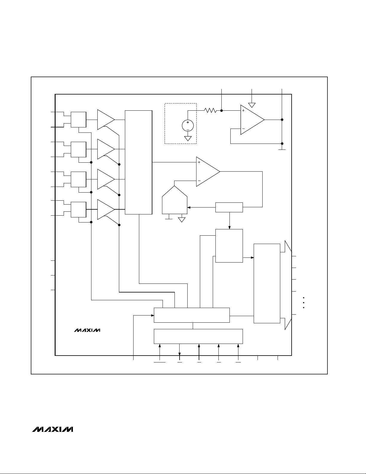
The MAX125/MAX126 use a successive-approximation
conversion technique and four simultaneous-sampling
track/hold (T/H) amplifiers to convert analog signals into
14-bit digital outputs. Each T/H has two multiplexed
inputs, allowing a total of eight inputs. Each T/H output
is converted and stored in memory to be accessed
sequentially by the parallel interface with successive
read cycles. The MAX125/MAX126 internal microsequencer can be programmed to digitize one, two,
three, or four inputs sampled simultaneously from either
of the two banks of four inputs (see Figure 2).
The conversion timing and control sequences are
derived from a 16MHz external clock, the CONVST
MAX125/MAX126
2x4-Channel, Simultaneous-Sampling
14-Bit DAS
6 _______________________________________________________________________________________
NAME FUNCTION
1, 2 CH2B, CH2A Channel 2 Multiplexed Inputs, single-ended
3, 4 CH1B, CH1A Channel 1 Multiplexed Inputs, single-ended
PIN
5 AV
DD
+5V ±5% Analog Supply Voltage
6 REFIN External Reference Input/Internal Reference Output. Bypass with a 0.1µF capacitor to AGND.
17 DV
DD
+5V ±5% Digital Supply Voltage
9–16 D13–D6 Data Bits. D13 = MSB.
8, 36 AGND Analog Ground. Both pins must be tied to ground.
7 REFOUT Reference-Buffer Output. Bypass with a 4.7µF capacitor to AGND.
26
CS
Chip-Select Input (active-low)
25 CLK Clock Input (duty cycle must be 30% to 70%).
21–24 D3/A3–D0/A0 Bidirectional Data Bits/Address Bits. D0/A0 = LSB.
19, 20 D5, D4 Data Bits
18 DGND Digital Ground
______________________________________________________________Pin Description
27
WR
Write Input (active-low)
28
RD
Read Input (active-low)
29
CONVST
Conversion-Start Input. Rising edge initiates sampling and conversion sequence.
30
INT
Interrupt Output. Falling edge indicates the end of a conversion sequence.
31 AV
SS
-5V ±5% Analog Supply Voltage
32, 33 CH4A, CH4B Channel 4 Multiplexed Inputs, single-ended
34, 35 CH3A, CH3B Channel 3 Multiplexed Inputs, single-ended
Figure 1. Load Circuit for Access Time and Bus Relinquish Time
TO OUTPUT
PIN
120pF
1.0mA
1.6mA
1.6V
Page 7
MAX125/MAX126
2x4-Channel, Simultaneous-Sampling
14-Bit DAS
_______________________________________________________________________________________ 7
MUX
2.50V
BANDGAP REFERENCE
REFIN
10k
AGND REFOUT
MUX
T/H
T/H
T/H
T/H
A
B
MUX
A
B
MUX
A
B
MUX
CH1A
CH1B
CH2A
CH2B
CH3A
CH3B
CH4A
CH4B
A
B
14-BIT
DAC
CONTROL LOGIC
BUS INTERFACE
CLK CONVST INT CS RD WR DV
DD
DGND
SAR
14x4
RAM
V
REF
THREE-STATE
OUTPUT
DRIVERS
AV
DD
AGND
AV
SS
D0/A0 (LSB)
D1/A1
D2/A2
D3/A3
D13 (MSB)
MAX125
MAX126
V
REF
COMP
Figure 2. Functional Diagram
Page 8
MAX125/MAX126
2x4-Channel, Simultaneous-Sampling
14-Bit DAS
8 _______________________________________________________________________________________
signal, and the programmed mode. The T/H amplifiers
hold the input voltages at the CONVST rising edge.
Additional CONVST pulses are ignored until the last
conversion for the sample is complete. The ADC converts each assigned channel in 3µs and stores the
result in an internal 4x14-bit memory.
At the end of the last conversion, INT goes low and the
T/H amplifiers begin to track the inputs again. The data
can be accessed by applying successive pulses to the
RD pin. Successive reads access data words sequentially. The memory is
not
random-access; data from
CH1 is always read first. After accessing all programmed channels, the address pointer selects CH1
again. Additional read pulses cycle through the data
words. CS can be held low during successive reads.
Input Bandwidth
The T/H’s input tracking circuitry has an 8MHz smallsignal bandwidth, so it is possible to digitize highspeed transient events and measure periodic signals
with bandwidths exceeding the ADC’s sampling rate by
using undersampling techniques. To avoid highfrequency signals being aliased into the frequency
band of interest, anti-alias filtering is recommended.
Analog Input Range and Input Protection
The MAX125’s input range is ±5V, and the MAX126’s
input range is ±2.5V. The input resistance for both parts
is 10kΩ. An input protection structure allows input volt-
ages to ±17V without harming the IC. This protection is
also active in shutdown mode.
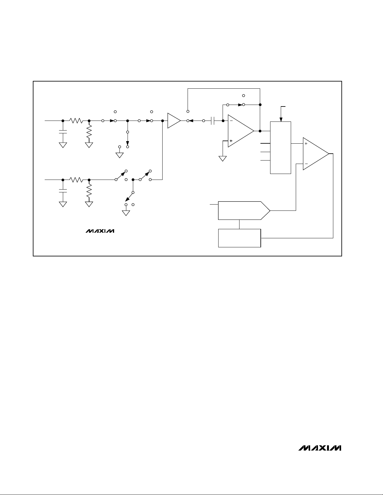
Track/Holds
The MAX125/MAX126 feature four simultaneous T/Hs.
Each T/H has two multiplexed inputs. A T-switch input
configuration provides excellent hold-mode isolation.
Allow 1µs acquisition time for 14-bit accuracy.
The T/H aperture delay is typically 10ns. The 500ps
aperture-delay mismatch between the T/Hs allows the
relative phase information of up to four different inputs
to be preserved. Figure 3 shows the equivalent input
circuit, illustrating the ADC’s sampling architecture.
Only one of four T/H stages with its two multiplexed
inputs (CH_A and CH_B) is shown. All switches are in
track configuration for channel A. An internal buffer
charges the hold capacitor to minimize the required
acquisition time between conversions. The analog input
appears as a 10kΩ resistor in parallel with a 16pF
capacitor.
C
IN
5k
C
IN
5k
S1A S2A
HOLD
BUFFER
TRACK
C
HOLD
7pF
HOLD
FROM MICROSEQUENCER
REFOUT
TRACK
MUX
DAC
SAR
S1B S2B
S3B
S3A
5k
5k
CH_A
CH_B
MAX125
MAX126
Figure 3. Equivalent Input Circuit
Page 9

Between conversions, the buffer input is connected to
channel 1 of the selected track/hold bank. When a
channel is not selected, switches S1, S2, and S3 are
placed in hold mode to improve channel-to-channel
isolation.
Digital Interface
Input data (A0–A3) and output data (D0–D13) are multiplexed on a three-state bidirectional interface. This parallel I/O can easily be interfaced with a microprocessor
(µP) or DSP. CS, WR, and RD control the write and read
operations. CS is the standard chip-select signal, which
enables the controller to address the MAX125/MAX126
as an I/O port. When CS is high, it disables the WR and
RD inputs and forces the interface into a high-Z state.
Figure 4 details the interface timing.
Programming Modes
The MAX125/MAX126 have eight conversion modes
plus power-down, which are programmed through a
bidirectional parallel interface. At power-up, the devices
default to the mode
Input Mux A/Single-Channel
Conversion.
The user can select between two banks
(mux inputs A or mux inputs B) of four simultaneoussampled input channels, as illustrated in Figure 2. An
internal microsequencer can be programmed to convert
one, two, three, or four channels of the selected bank
per sample. For a single-channel conversion, CH1 is
digitized, and then INT goes low to indicate completion
of the conversion. For multichannel conversions, INT
goes low after the last channel has been digitized.
To input data into the MAX125/MAX126, pull CS low,
program the bidirectional pins A0–A3 (Table 1), and
pulse WR low. Data is latched into the devices on the
WR or CS rising edge. The ADC is now ready to convert.
Once programmed, the ADCs continue operating in the
same mode until they are reprogrammed or until power
is removed. Figure 5 shows an example of programming a four-channel conversion using Input Mux A.
Starting a Conversion
After programming the MAX125/MAX126 as outlined in
the
Programming Modes
section, pulse CONVST low to
initiate a conversion sequence. The analog inputs are
sampled at the CONVST rising edge. Do not start a
new conversion while the conversion is in progress.
Monitor the INT output. A falling edge indicates the end
of a conversion sequence.
MAX125/MAX126
2x4-Channel, Simultaneous-Sampling
14-Bit DAS
_______________________________________________________________________________________ 9
CH1 CH2 CH3 CH4
t
ACQ
t
CONV
t
AH
t
AS
t
WR
t
CSD
t
CWH
t
DH
t
DA
t
RD
t
CRS
t
CRH
t
RD
t
ID
t
CWS
CONVST
INT
CS
WR
DATA
t
CW
DATA IN
RD
Figure 4. Timing Diagram
Figure 5. Programming a Four-Channel Conversion, Input Mux A
A0
(LSB)
WR
CS
A1
A2
A3
Page 10

MAX125/MAX126
Reading a Conversion
Digitized data from up to four channels are stored in
memory to be read out through the parallel interface.
After receiving an INT signal, the user can access up to
four conversion results by performing up to four read
operations.
With CS low, the conversion result from CH_1 is
accessed, and INT is reset high on the first RD falling
edge. On the RD rising edge, the internal address
pointer is advanced. If a single conversion is programmed, only one RD pulse is required, and the
address pointer is reset to CH_1. For multichannel conversions, up to four RD falling edges sequentially
access the data for channels 1 through 4. For
n
chan-
nels converted (1 <
n
≤ 4), the address pointer is reset
to CH_1 after nRD pulses. Do not perform a read operation during conversion, as it will corrupt the conversion’s accuracy.
__________Applications Information
External Clock
The MAX125/MAX126 require a TTL-compatible clock
up to 16MHz for proper operation. The clock duty
cycle’s range is between 30% and 70%.
Internal and External Reference
The MAX125/MAX126 can be used with an internal or
external reference voltage. An external reference can
be connected directly at REFIN. An internal buffer with
a gain of +1 provides 2.5V at REFOUT.
Internal Reference
The full-scale range with the internal reference is ±5V
for the MAX125 and ±2.5V for the MAX126. Bypass
REFIN with a 0.1µF capacitor to AGND and bypass the
REFOUT pin with a 4.7µF (min) capacitor to AGND
(Figure 6). The maximum value to compensate the reference buffer is 22µF. Larger values are acceptable if
low-ESR capacitors are used.
External Reference
For operation over a wide temperature range, an external 2.5V reference with tighter specifications improves
accuracy. The MAX6325 is an excellent choice
to match the MAX125/MAX126 accuracy over the
commercial and extended temperature ranges with a
2x4-Channel, Simultaneous-Sampling
14-Bit DAS
10 ______________________________________________________________________________________
X = Don’t care
Table 1. Modes of Operation
A3 A2 A1
0 0 0
0 0 0
0 0 1
0 0 1
A0
0
1
0
1
CONVERSION
TIME (µs)
3
6
9
12
MODE
Input Mux A/Two-Channel Conversion
Input Mux A/Three-Channel Conversion
Input Mux A/Four-Channel Conversion
0 1 0 0 3 Input Mux B/Single-Channel Conversion
0 1 0 1 6 Input Mux B/Two-Channel Conversion
0 1 1 0 9 Input Mux B/Three-Channel Conversion
0 1 1 1 12 Input Mux B/Four-Channel Conversion
1 X X X — Power-Down
TO DAC
REFIN
10k
0.1µF
4.7µF
A
V
= 1
2.5V
REFOUT 76(2.5V)
(2.5V)
MAX125
MAX126
Figure 6. Internal Reference
Input Mux A/Single-Channel Conversion (default at power-up)
Page 11
1ppm/°C (max) temperature drift. Connect an external
reference at REFIN as shown in Figure 7. The minimum
impedance is 7kΩ for DC currents in both normal oper-
ation and shutdown. Bypass REFOUT with a 4.7µF lowESR capacitor.
Power-On Reset
When power is first applied, the internal power-on-reset
circuitry activates the MAX125/MAX126 with INT =
high, ready to convert. The default conversion mode is
Input Mux A/Single-Channel Conversion. See the
Programming Modes
section if other configurations are
desired.
After the power supplies have been stabilized, the reset
time is 5µs; no conversions should be performed
during this phase. At power-up, data in memory is
undefined.
Software Power-Down
Software power-down is activated by setting bit A3 of
the control word high (Table 1). It is asserted after the
WR or CS rising edge, at which point the ADC immedi-
ately powers down to a low quiescent-current state.
AVDDdrops to less than 1.5mA, and AVSSis reduced
to less than 1mA. The ADC blocks and reference buffer
are turned off, but the digital interface and the reference remain active for fast power-up recovery. Wake
up the MAX125/MAX126 by writing a control word
(A0–A3, Table 1). The bidirectional interface interprets
a logic zero at A3 as the start signal and powers up in
the mode selected by A0, A1, and A2. The reference
buffer’s settling time and the bypass capacitor’s value
dominate the power-up delay. With the recommended
4.7µF at REFOUT, the power-up delay is typically 5µs.
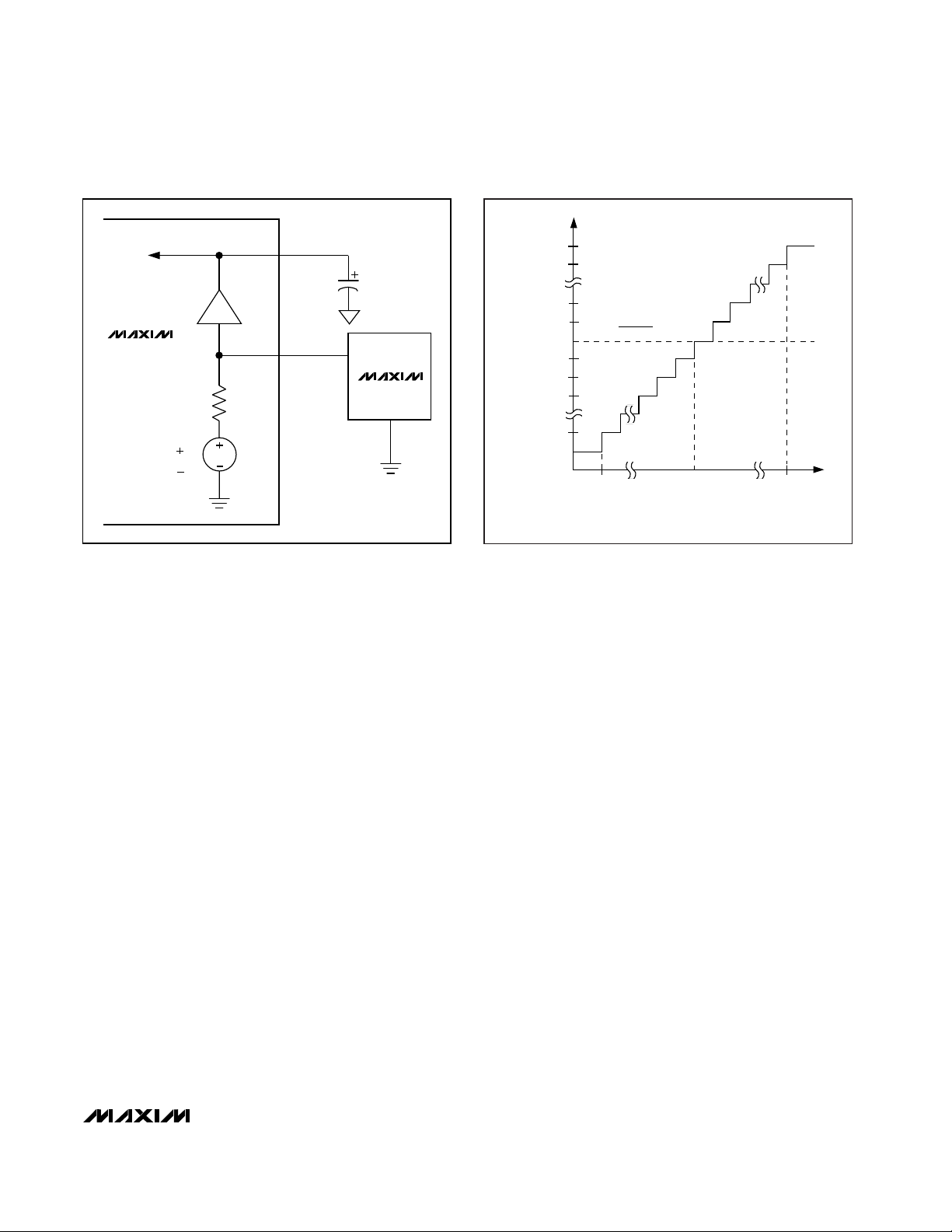
Transfer Function
The MAX125/MAX126 have bipolar input ranges. Figure 8 shows the bipolar/output transfer function. Code
transitions occur at successive-integer least significant
bit (LSB) values. Output coding is twos-complement
binary with 1LSB = 610µV for the MAX125 and
1LSB = 305µV for the MAX126.
Output Demultiplexer
An output demultiplexer circuit is useful for isolating
data from one channel in a four-channel conversion
sequence. Figure 9’s circuit uses the external 16MHz
clock and the INT signal to generate four RD pulses
and a latch clock to save data from the desired channel. CS must be low during the four RD pulses. The
channel is selected with the binary coding of two
switches. A 16-bit 16373 latch simplifies layout.
Motor-Control Applications
Vector motor control requires monitoring of the individual phase currents. In their most basic application, the
MAX125/MAX126 simultaneously sample two currents
(CH1A and CH2A, Figure 10) and preserve the necessary relative phase information. Only two of the three
phase currents have to be digitized, because the third
component can be mathematically derived with a coordinate transformation.
MAX125/MAX126
2x4-Channel, Simultaneous-Sampling
14-Bit DAS
______________________________________________________________________________________ 11
TO DAC
REFIN
10k
4.7µF
A
V
= 1
2.5V
REFOUT 76(2.5V)
(2.5V)
OUT
MAX6325
MAX125
MAX126
Figure 7. External Reference
011 . . . 111
011 . . . 110
000 . . . 010
000 . . . 001
000 . . . 000
111 . . . 111
111 . . . 110
111 . . . 101
100 . . . 001
100 . . . 000
- FS
ZERO
INPUT VOLTAGE (LSB)
FS = 2 x V
REFOUT
(MAX125)
FS = V
REFOUT
(MAX126)
OUTPUT CODE
+FS - 1LSB
1LSB =
4V
REFOUT
16384
Figure 8. Bipolar Transfer Function
Page 12

MAX125/MAX126
The circuit of Figure 10 shows a typical vector motorcontrol application using all available inputs of the
MAX125/MAX126. CH1A and CH2A are connected
to two isolated Hall-effect current sensors and are a
part of the current (torque) feedback loop. The
MAX125/MAX126 digitize the currents and deliver raw
data to the following DSP and controller stages, where
the vector processing takes place. Sensorless vector
control uses a computer model for the motor and an
algorithm to split each output current into its magnetizing (stator current) and torque-producing (rotor current)
components.
If a 2- to 3-phase conversion is not practical, three currents can be sampled simultaneously with the addition
of a third sensor (not shown). Optional voltage
(position) feedback can be derived by measuring two
phase voltages (CH3A, CH4A). Typically, an isolated
differential amplifier is used between the motor and the
MAX125/MAX126. Again, the third phase voltage can
be derived from the magnitude (phase voltage) and its
relative phase.
For optimum speed control and good load regulation
close to zero speed, additional velocity and position
feedback are derived from an encoder or resolver and
2x4-Channel, Simultaneous-Sampling
14-Bit DAS
12 ______________________________________________________________________________________
PRE
CLR
HC161
1/2 HC74
V
CC
V
CC
V
CC
ENP
ENT
LOAD
A
B
C
D
(LSB) 0
1
2
3
RCO
D Q
Q
CLR
P0
P1
P2
P3
P4
P5
P6
P7
HC688
P = Q
Q0
Q1
Q2
V
CC
Q3
Q4
Q5
Q6
Q7
G
LATCH
CLOCK
(TO 16373 LATCH)
0CH1 0
1CH2 0
0CH3 1
1CH4 1
10k
EXTERNAL
CLOCK
EXTERNAL
CLOCK
RD
INT
Figure 9. Output Demultiplexer Circuit
Page 13

MAX125/MAX126
2x4-Channel, Simultaneous-Sampling
14-Bit DAS
______________________________________________________________________________________ 13
Figure 10. Vector Motor Control
brought to the MAX125/MAX126 at CH4B. The additional channels can be used to evaluate slower analog
inputs, such as the main DC bus voltage (CH2B), temperature sensors (CH3B), or other analog inputs (AUX,
CH1B).
Power-Supply Bypassing
and Ground Management
For optimum system performance, use printed circuit
boards with separate analog and digital ground
planes. Wire-wrapped boards are not recommended.
Connect the two ground planes together at the lowimpedance power-supply source. Connect DGND and
AGND together at the IC. For the best ground connection, connect the DGND and AGND pins together and
connect that point to the system analog ground plane
to avoid interference from other digital noise sources. If
DGND is connected to the system digital ground, digital noise may get through to the ADC’s analog portion.
The AGND pins must be connected directly to a lowimpedance ground plane. Extra impedance between
the pins and the ground plane increases crosstalk and
degrades INL.
Bypass AV
DD
and AVSSwith 0.1µF ceramic capacitors
to AGND. Mount them with short leads close to the
device. Ferrite beads may also be used to further isolate the analog and digital power supplies. Bypass
DVDDwith a 0.1µF ceramic capacitor to DGND.
MAIN DC
14 BIT ADC +
MICRO-
SEQUENCER
CH1
CH2
CH3
CH4
A
B
A
B TEMP
A
B
A
B AUX
MAIN DC
CURRENT/TORQUE
FEEDBACK
VOLTAGE/POSITION
FEEDBACK
VELOCITY
FEEDBACK
AC
MOTOR
SIMULTANEOUS T/H
MAX125
MAX126
AC
MOTOR
R/E
RESOLVER/
ENCODER
µC
DSP
14
BUFFER
POWER
STAGE
CONTROLLER
EXTERNAL
SETPOINTS
Page 14

MAX125/MAX126
2x4-Channel, Simultaneous-Sampling
14-Bit DAS
14 ______________________________________________________________________________________
36
35
34
33
32
31
30
29
28
27
26
25
24
23
1
2
3
4
5
6
7
8
9
10
11
12
13
14
AGND
CH3B
CH3A
CH4B
CH4A
AV
SS
D1/A1
INT
CONVST
RD
WR
CS
CLK
D0/A0 (LSB)
D8
D9
D10
D11
D12
D13 (MSB)
AGND
REFOUT
REFIN
AV
DD
CH1A
CH1B
CH2A
CH2B
SSOP
TOP VIEW
MAX125
MAX126
22
21
20
19
15
16
17
18 D5
D2/A2
D3/A3
D4
DGND
DV
DD
D6
D7
__________________Pin Configuration
D0/A0
D1/A1
D2/A2
D3/A3
D4
D5
D6
D7
D8
D9
D10
D11
D12
D13
CH1A
CH1B
CH2A
CH2B
CH3A
CH3B
CH4A
CH4B
MAX125
MAX126
CONVST
CONTROL INTERFACE
CLK
REFOUT DGND
AGND
REFIN DV
DD
4.7µF
16MHz
0.1µF
0.1µF
-5V
0.1µF
+5V
0.1µF
+5V
AV
SS
AV
DD
INT CS RD WR
__________Typical Operating Circuit
TRANSISTOR COUNT: 4219
SUBSTRATE CONNECTED TO AV
SS
___________________Chip Information
Page 15
MAX125/MAX126
2x4-Channel, Simultaneous-Sampling
14-Bit DAS
Maxim cannot assume responsibility for use of any circuitry other than circuitry entirely embodied in a Maxim product. No circuit patent licenses are
implied. Maxim reserves the right to change the circuitry and specifications without notice at any time.
Maxim Integrated Products, 120 San Gabriel Drive, Sunnyvale, CA 94086 408-737-7600 ____________________
15
© 2007 Maxim Integrated Products is a registered trademark of Maxim Integrated Products, Inc.
Revision History
Pages changed at Rev 2: 1, 2, 15
Package Information
(The package drawing(s) in this data sheet may not reflect the most current specifications. For the latest package outline information
go to www.maxim-ic.com/packages
.)
36
1
TOP VIEW
e
MAX
0.104
0.011
0.017
0.013
0.299
0.040
MILLIMETERS
MAX
MIN
2.65
2.44
0.29
0.10
0.44
0.30
0.23
0.32
7.40 7.60
0.51 1.02
15.20 15.55
0∞-8∞
INCHES
MIN
DIM
0.096A
0.004
A1
0.012
B
0.009
C
HE
D
A1
A
B
C
e 0.0315 BSC 0.80 BSC
0.291
E
H 0.4140.398 10.11 10.51
0.020L
D 0.6120.598
L
SSOP.EPS
FRONT VIEW
SIDE VIEW
PROPRIETARY INFORMATION
TITLE:
PACKAGE OUTLINE, 36L SSOP, 0.80 MM PITCH
REV.DOCUMENT CONTROL NO.APPROVAL
21-0040 E
1
1
 Loading...