

General Description
The MAX12558 is a dual, 3.3V, 14-bit analog-to-digital
converter (ADC) featuring fully differential wideband
track-and-hold (T/H) inputs, driving internal quantizers.
The MAX12558 is optimized for low power, small size,
and high dynamic performance in intermediate frequency (IF) and baseband sampling applications. This dual
ADC operates from a single 3.3V supply, consuming
only 756mW while delivering a typical 71.7dB signal-tonoise ratio (SNR) performance at a 175MHz input frequency. The T/H input stages accept single-ended or
differential inputs up to 400MHz. In addition to low operating power, the MAX12558 features a 330µW powerdown mode to conserve power during idle periods.
A flexible reference structure allows the MAX12558 to
use the internal 2.048V bandgap reference or accept
an externally applied reference and allows the reference to be shared between the two ADCs. The reference structure allows the full-scale analog input range
to be adjusted from ±0.35V to ±1.15V. The MAX12558
provides a common-mode reference to simplify design
and reduce external component count in differential
analog input circuits.
The MAX12558 supports either a single-ended or differential input clock. User-selectable divide-by-two (DIV2)
and divide-by-four (DIV4) modes allow for design flexibility and help to reduce the negative effects of clock jitter.
Wide variations in the clock duty cycle are compensated
with the ADC’s internal duty-cycle equalizer (DCE).
The MAX12558 features two parallel, 14-bit-wide,
CMOS-compatible outputs. The digital output format is
pin-selectable to be either two’s complement or Gray
code. A separate power-supply input for the digital outputs accepts a 1.7V to 3.6V voltage for flexible interfacing with various logic levels. The MAX12558 is available
in a 10mm x 10mm x 0.8mm, 68-pin thin QFN package
with exposed paddle (EP), and is specified for the
extended (-40°C to +85°C) temperature range.
For a 12-bit, pin-compatible version of this ADC, refer to
the MAX12528 data sheet. See the Selector Guide for
more selections.
Applications
IF and Baseband Communication Receivers
Cellular, LMDS, Point-to-Point Microwave,
MMDS, HFC, WLAN
I/Q Receivers
Ultrasound and Medical Imaging
Portable Instrumentation
Digital Set-Top Boxes
Low-Power Data Acquisition
Features
♦ Direct IF Sampling Up to 400MHz
♦ Excellent Dynamic Performance
74.4dB/71.7dB SNR at f
IN
= 70MHz/175MHz
84.2dBc/79dBc SFDR at f
IN
= 70MHz/175MHz
♦ 3.3V Low-Power Operation
789mW (Differential Clock Mode)
756mW (Single-Ended Clock Mode)
♦ Fully Differential or Single-Ended Analog Input
♦ Adjustable Differential Analog Input Voltage
♦ 750MHz Input Bandwidth
♦ Adjustable, Internal or External, Shared Reference
♦ Differential or Single-Ended Clock
♦ Accepts 25% to 75% Clock Duty Cycle
♦ User-Selectable DIV2 and DIV4 Clock Modes
♦ Power-Down Mode
♦ CMOS Outputs in Two’s Complement or Gray
Code
♦ Out-of-Range and Data-Valid Indicators
♦ Small, 68-Pin Thin QFN Package
(10mm x 10mm x 0.8mm)
♦ 12-Bit, Pin-Compatible Version Available
(MAX12528)
♦ Evaluation Kit Available (Order MAX12558EVKIT)
MAX12558
Dual, 80Msps, 14-Bit, IF/Baseband ADC
________________________________________________________________ Maxim Integrated Products 1
Ordering Information
19-3842; Rev 0; 10/05
For pricing, delivery, and ordering information, please contact Maxim/Dallas Direct! at
1-888-629-4642, or visit Maxim’s website at www.maxim-ic.com.
EVALUATION KIT
AVAILABLE
*EP = Exposed paddle.
+Denotes lead-free package.
**Future product—contact factory for availability.
PART
SAMPLING RATE
(Msps)
RESOLUTION
(Bits)
MAX12559** 95 14
MAX12558 80 14
MAX12557 65 14
MAX12529** 95 12
MAX12528 80 12
MAX12527 65 12
Selector Guide
Pin Configuration appears at end of data sheet.
PART TEMP RANGE PIN-PACKAGE
MAX12558ETK -40°C to +85°C 68 Thin QFN-EP* T6800-2
MAX12558ETK+ -40°C to +85°C 68 Thin QFN-EP* T6800-2
PKG
CODE
MAX12558
Dual, 80Msps, 14-Bit, IF/Baseband ADC
2 _______________________________________________________________________________________
ABSOLUTE MAXIMUM RATINGS
ELECTRICAL CHARACTERISTICS
(VDD= 3.3V, OVDD= 2.0V, GND = 0, REFIN = REFOUT (internal reference), CL≈ 10pF at digital outputs, VIN= -1dBFS (differential),
DIFFCLK/SECLK = OV
DD
, PD = GND, SHREF = GND, DIV2 = GND, DIV4 = GND, G/T = GND, f
CLK
= 80MHz (50% duty cycle), TA=
-40°C to +85°C, unless otherwise noted. Typical values are at T
A
= +25°C.) (Note 1)
Stresses beyond those listed under “Absolute Maximum Ratings” may cause permanent damage to the device. These are stress ratings only, and functional
operation of the device at these or any other conditions beyond those indicated in the operational sections of the specifications is not implied. Exposure to
absolute maximum rating conditions for extended periods may affect device reliability.
VDDto GND ................................................................-0.3V to +3.6V
OV
DD
to GND............-0.3V to the lower of (VDD+ 0.3V) and +3.6V
INAP, INAN to GND ...-0.3V to the lower of (V
DD
+ 0.3V) and +3.6V
INBP, INBN to GND ...-0.3V to the lower of (V
DD
+ 0.3V) and +3.6V
CLKP, CLKN to
GND ........................-0.3V to the lower of (V
DD
+ 0.3V) and +3.6V
REFIN, REFOUT
to GND ..................-0.3V to the lower of (V
DD
+ 0.3V) and +3.6V
REFAP, REFAN,
COMA to GND ......-0.3V to the lower of (V
DD
+ 0.3V) and +3.6V
REFBP, REFBN,
COMB to GND ......-0.3V to the lower of (V
DD
+ 0.3V) and +3.6V
DIFFCLK/SECLK, G/T, PD, SHREF, DIV2,
DIV4 to GND .........-0.3V to the lower of (V
DD
+ 0.3V) and +3.6V
D0A–D13A, D0B–D13B, DAV,
DORA, DORB to GND..............................-0.3V to (OV
DD
+ 0.3V)
Continuous Power Dissipation (T
A
= +70°C)
68-Pin Thin QFN, 10mm x 10mm x 0.8mm
(derate 70mW/°C above +70°C) ....................................4000mW
Operating Temperature Range................................-40°C to +85°C
Junction Temperature ...........................................................+150°C
Storage Temperature Range .................................-65°C to +150°C
Lead Temperature (soldering 10s).......................................+300°C
PARAMETER SYMBOL CONDITIONS MIN TYP MAX UNITS
DC ACCURACY
Resolution 14 Bits
Integral Nonlinearity INL fIN = 3MHz ±1.4 LSB
Differential Nonlinearity DNL
Offset Error ±0.1 ±0.7 %FSR
Gain Error External reference, V
ANALOG INPUT (INAP, INAN, INBP, INBN)
Differential Input Voltage Range V
Common-Mode Input Voltage V
Analog Input Resistance R
Analog Input Capacitance
CONVERSION RATE
Maximum Clock Frequency f
Minimum Clock Frequency 5 MHz
Data Latency Figure 5 8
DYNAMIC CHARACTERISTICS
Small-Signal Noise Floor SSNF Input at -35dBFS 75.4 76.8 dBFS
Signal-to-Noise Ratio SNR
= 3MHz, no missing codes over
f
IN
temperature (Note 2)
DIFF
C
PAR
C
SAMPLE
CLK
Differential or single-ended inputs ±1.024 V
Each input, Figure 3 2.8 kΩ
IN
Fixed capacitance to ground,
each input, Figure 3
Switched capacitance,
each input, Figure 3
fIN = 3MHz 72.7 75.2
fIN = 40MHz 74.7
fIN = 70MHz 74.4
= 175MHz 69.9 71.7
f
IN
= 2.048V ±0.1 ±4.6 %FSR
REFIN
-1.0 ±0.6 +1.2 LSB
/ 2 V
DD
2
4.5
80 MHz
pF
Clock
Cycles
dB
MAX12558
Dual, 80Msps, 14-Bit, IF/Baseband ADC
_______________________________________________________________________________________ 3
ELECTRICAL CHARACTERISTICS (continued)
(VDD= 3.3V, OVDD= 2.0V, GND = 0, REFIN = REFOUT (internal reference), CL≈ 10pF at digital outputs, VIN= -1dBFS (differential),
DIFFCLK/SECLK = OV
DD
, PD = GND, SHREF = GND, DIV2 = GND, DIV4 = GND, G/T = GND, f
CLK
= 80MHz (50% duty cycle), TA=
-40°C to +85°C, unless otherwise noted. Typical values are at T
A
= +25°C.) (Note 1)
PARAMETER SYMBOL CONDITIONS MIN TYP MAX UNITS
Signal-to-Noise Plus Distortion SINAD
Spurious-Free Dynamic Range SFDR
Total Harmonic Distortion THD
Second Harmonic HD2
Third Harmonic HD3
3rd-Order Intermodulation
Distortion IM3
Full-Power Bandwidth FPBW Input at -0.2dBFS, -3dB rolloff 750
Aperture Delay
Aperture Jitter t
Output Noise n
t
AD
AJ
OUT
fIN = 3MHz 71.1 74.8
fIN = 40MHz 73.5
fIN = 70MHz 73.7
f
= 175MHz 68.6 70.6
IN
fIN = 3MHz 73.8 86.9
fIN = 40MHz 81.9
fIN = 70MHz 84.2
= 175MHz 72.8 79
f
IN
fIN = 3MHz -85.3 -72.9
fIN = 40MHz -79.7
fIN = 70MHz -81.7
= 175MHz -77.1 -71.3
f
IN
fIN = 3MHz -87.3
fIN = 40MHz -84.8
fIN = 70MHz -86.7
f
= 175MHz -79.9
IN
fIN = 3MHz -91.4
fIN = 40MHz -81.9
fIN = 70MHz -84.3
f
= 175MHz -81.3
IN
f
= 68.5MHz at -7dBFS
IN1
= 71.5MHz at -7dBFS
f
IN2
= 172.5MHz at -7dBFS
f
IN1
= 177.5MHz at -7dBFS
f
IN2
Figure 5 1.2 ns
INAP = INAN = COMA
INBP = INBN = COMB
-86.5
-87.1
< 0.1
0.91 LSB
dBc
dBc
dBc
dBc
dBc
MHz
ps
dB
RMS
RMS
MAX12558
Dual, 80Msps, 14-Bit, IF/Baseband ADC
4 _______________________________________________________________________________________
ELECTRICAL CHARACTERISTICS (continued)
(VDD= 3.3V, OVDD= 2.0V, GND = 0, REFIN = REFOUT (internal reference), CL≈ 10pF at digital outputs, VIN= -1dBFS (differential),
DIFFCLK/SECLK = OV
DD
, PD = GND, SHREF = GND, DIV2 = GND, DIV4 = GND, G/T = GND, f
CLK
= 80MHz (50% duty cycle), TA=
-40°C to +85°C, unless otherwise noted. Typical values are at T
A
= +25°C.) (Note 1)
PARAMETER SYMBOL CONDITIONS MIN TYP MAX UNITS
Overdrive Recovery Time ±10% beyond full scale 1
INTERCHANNEL CHARACTERISTICS
Crosstalk Rejection
Gain Matching ±0.01 ±0.1 dB
Offset Matching ±0.01 %FSR
INTERNAL REFERENCE (REFOUT)
REFOUT Output Voltage V
REFOUT Load Regulation -1mA < I
REFOUT Temperature Coefficient TC
REFOUT Short-Circuit Current
BUFFERED REFERENCE MODE (REFIN is driven by REFOUT or an external 2.048V single-ended reference source;
V
REFAP/VREFAN/VCOMA
REFIN Input Voltage V
REFIN Input Resistance R
COM_ Output Voltage
REF_P Output Voltage
REF_N Output Voltage
Differential Reference Voltage
Differential Reference
Temperature Coefficient
UNBUFFERED EXTERNAL REFERENCE (REFIN = GND, V
externally, V
COMA
REF_P Input Voltage
REF_N Input Voltage
COM_ Input Voltage V
Differential Reference Voltage
REFOUT
REF
f
INA
f
INA
or f
or f
= 70MHz at -1dBFS 95
INB
= 175MHz at -1dBFS 87
INB
< +1mA 35 mV/mA
REFOUT
Short to VDD—sinking 0.24
Short to GND—sourcing 2.1
= V
and V
COMB
REFBP/VREFBN/VCOMB
REFIN
REFIN
V
COMA
V
COMB
V
REFAP
V
REFBP
V
REFAN
V
REFBN
V
REFA
V
REFB
TC
REF
= VDD / 2)
V
REFAP
V
REFBP
V
REFAN
V
REFBN
COM_
V
REFA
V
REFB
are generated internally)
V
= VDD / 2 1.60 1.65 1.70 V
COM_
V
= VDD / 2 + (V
REF_P
V
= VDD / 2 - (V
REF_N
V
= V
REF_
V
- V
REF_P
V
- V
REF_N
V
= VDD / 2 1.65 V
COM_
V
= V
REF_
- V
REF_P
COM_
COM_
REF_P
REF_N
REFAP/VREFAN/VCOMA
- V
REF_N
x 3/8) 2.418 V
REFIN
x 3/8) 0.882 V
REFIN
= V
REFIN
2.000 2.048 2.080 V
±50 ppm/°C
2.048 V
> 50 MΩ
1.456 1.536 1.595 V
±25 ppm/°C
and V
REFBP/VREFBN/VCOMB
are applied
+0.768 V
-0.768 V
x 3/4 1.536 V
Clock
Cycle
dB
mA
MAX12558
Dual, 80Msps, 14-Bit, IF/Baseband ADC
_______________________________________________________________________________________ 5
ELECTRICAL CHARACTERISTICS (continued)
(VDD= 3.3V, OVDD= 2.0V, GND = 0, REFIN = REFOUT (internal reference), CL≈ 10pF at digital outputs, VIN= -1dBFS (differential),
DIFFCLK/SECLK = OV
DD
, PD = GND, SHREF = GND, DIV2 = GND, DIV4 = GND, G/T = GND, f
CLK
= 80MHz (50% duty cycle), TA=
-40°C to +85°C, unless otherwise noted. Typical values are at T
A
= +25°C.) (Note 1)
PARAMETER SYMBOL CONDITIONS MIN TYP MAX UNITS
REF_P Sink Current
REF_N Source Current
COM_ Sink Current
REF_P, REF_N Capacitance
COM_ Capacitance C
CLOCK INPUTS (CLKP, CLKN)
Single-Ended Input High
Threshold
Single-Ended Input Low
Threshold
Minimum Differential Clock Input
Voltage Swing
Differential Input Common-Mode
Voltage
CLKP, CLKN Input Resistance R
CLKP, CLKN Input Capacitance C
DIGITAL INPUTS (DIFFCLK/SECLK, G/T, PD, DIV2, DIV4, SHREF)
Input High Threshold V
Input Low Threshold V
Input Leakage Current
Digital Input Capacitance C
DIGITAL OUTPUTS (D0A–D13A, D0B–D13B, DORA, DORB, DAV)
Output-Voltage Low V
Output-Voltage High V
Tri-State Leakage Current
(Note 3)
I
REFAP
I
REFBP
I
REFAN
I
REFBN
I
COMA
I
COMB
C
REF_P
C
REF_N
COM_
V
V
CLK
CLK
V
REF_P
V
REF_N
V
= 1.65V 0.85 mA
COM_
,
DIFFCLK/SECLK = GND, CLKN = GND
IH
DIFFCLK/SECLK = GND, CLKN = GND
IL
DIFFCLK/SECLK = OV
DIFFCLK/SECLK = OV
Each input, Figure 4 5 kΩ
IH
IL
= 2.418V 1.2 mA
= 0.882V 0.85 mA
DD
DD
OVDD applied to input ±5
Input connected to ground ±5
DIN
D0A–D13A, D0B–D13B, DORA, DORB:
I
= 200µA
OL
SINK
DAV: I
= 600µA 0.2
SINK
D0A–D13A, D0B–D13B, DORA, DORB:
OH
I
LEAK
I
DAV: I
OVDD applied to input ±5
Input connected to ground ±5
SOURCE
SOURCE
= 200µA
= 600µA
13 pF
6pF
0.8 x
V
DD
0.2 x
V
DD
0.2 V
V
/ 2 V
DD
2pF
0.8 x
OV
DD
0.2 x
OV
DD
5pF
0.2
-
OV
DD
0.2
OV
-
DD
0.2
V
V
P-P
V
V
µA
V
V
µA
MAX12558
Dual, 80Msps, 14-Bit, IF/Baseband ADC
6 _______________________________________________________________________________________
ELECTRICAL CHARACTERISTICS (continued)
(VDD= 3.3V, OVDD= 2.0V, GND = 0, REFIN = REFOUT (internal reference), CL≈ 10pF at digital outputs, VIN= -1dBFS (differential),
DIFFCLK/SECLK = OV
DD
, PD = GND, SHREF = GND, DIV2 = GND, DIV4 = GND, G/T = GND, f
CLK
= 80MHz (50% duty cycle), TA=
-40°C to +85°C, unless otherwise noted. Typical values are at T
A
= +25°C.) (Note 1)
PARAMETER SYMBOL CONDITIONS MIN TYP MAX UNITS
D 0A–D 13A, D O RA,
D 0B–D 13B, and D O RB Tr i - S tate
O utp ut C ap aci tance ( N ote 3)
DAV Tri-State Output
Capacitance (Note 3)
POWER REQUIREMENTS
Analog Supply Voltage V
Digital Output Supply Voltage OV
Analog Supply Current I
Analog Power Dissipation P
Digital Output Supply Current I
C
OUT
C
DAV
DD
VDD
VDD
OVDD
DD
Normal operating mode
f
= 175MHz
IN
single-ended clock
(DIFFCLK/SECLK = GND)
Normal operating mode
= 175MHz
f
IN
differential clock
(DIFFCLK/SECLK = OV
Power-down mode (PD = OVDD)
clock idle
Normal operating mode
f
= 175MHz
IN
single-ended clock
(DIFFCLK/SECLK = GND)
Normal operating mode
= 175MHz
f
IN
differential clock
(DIFFCLK/SECLK = OV
Power-down mode (PD = OVDD)
clock idle
Normal operating mode
= 175MHz, C
f
IN
Power-down mode (PD = OVDD)
clock idle
)
DD
)
DD
L ≈ 10pF
3pF
6pF
3.15 3.30 3.60 V
1.70 2.0 V
229
239 273
0.1
756
789 900
0.33
22.6
0.004
DD
V
mA
mW
mA
MAX12558
Dual, 80Msps, 14-Bit, IF/Baseband ADC
_______________________________________________________________________________________ 7
ELECTRICAL CHARACTERISTICS (continued)
(VDD= 3.3V, OVDD= 2.0V, GND = 0, REFIN = REFOUT (internal reference), CL≈ 10pF at digital outputs, VIN= -1dBFS (differential),
DIFFCLK/SECLK = OV
DD
, PD = GND, SHREF = GND, DIV2 = GND, DIV4 = GND, G/T = GND, f
CLK
= 80MHz (50% duty cycle), TA=
-40°C to +85°C, unless otherwise noted. Typical values are at T
A
= +25°C.) (Note 1)
Note 1: Specifications ≥ +25°C guaranteed by production test, < +25°C guaranteed by design and characterization.
Note 2: Guaranteed by design and characterization. Device tested for performance during production test.
Note 3: During power-down, D0A–D13A, D0B–D13B, DORA, DORB, and DAV are high impedance.
Note 4: Data outputs settle to V
IH
or VIL.
Note 5: Guaranteed by design and characterization.
Typical Operating Characteristics
(VDD= 3.3V, OVDD= 2.0V, GND = 0, REFIN = REFOUT (internal reference), CL≈ 5pF at digital outputs, VIN= -1dBFS (differential),
DIFFCLK/SECLK = OV
DD
, PD = GND, G/T = GND, f
CLK
= 80MHz (50% duty cycle), TA= +25°C, unless otherwise noted.)
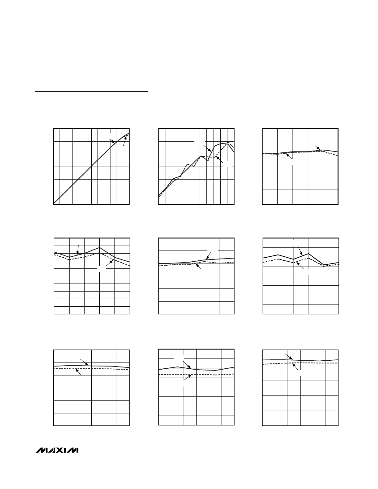
FFT PLOT (32,768-POINT DATA RECORD)
MAX12558 toc01
ANALOG INPUT FREQUENCY (MHz)
AMPLITUDE (dBFS)
-100
-80
-60
-40
-20
0
-120
HD3
f
CLK
= 80MHz
f
IN
= 3.00883MHz
A
IN
= -1.013dBFS
SNR = 75.3dB
SINAD = 75.1dB
THD = -90.1dBc
SFDR = 91.8dBc
HD2 = -91.8dBc
HD3 = -102dBc
HD2
-10
-30
-50
-70
-90
-110
35
25 403015 201050
FFT PLOT (32,768-POINT DATA RECORD)
MAX12558 toc02
ANALOG INPUT FREQUENCY (MHz)
AMPLITUDE (dBFS)
-100
-80
-60
-40
-20
0
-120
HD3
f
CLK
= 80MHz
f
IN
= 39.50928MHz
A
IN
= -1.024dBFS
SNR = 74.4dB
SINAD = 73.5dB
THD = -80.8dBc
SFDR = 83.3dBc
HD2 = -85.5dBc
HD3 = -82.6dBc
HD2
-10
-30
-50
-70
-90
-110
35
25 403015 201050
FFT PLOT (32,768-POINT DATA RECORD)
MAX12558 toc03
ANALOG INPUT FREQUENCY (MHz)
AMPLITUDE (dBFS)
-100
-80
-60
-40
-20
0
-120
f
CLK
= 80MHz
f
IN
= 70.09846MHz
A
IN
= -1.03dBFS
SNR = 74.2dB
SINAD = 73.7dB
THD = -83.3dBc
SFDR = 85.8dBc
HD2 = -88.7dBc
HD3 = -85.8dBc
-10
-30
-50
-70
-90
-110
HD3
HD2
3525 403015 201050
PARAMETER SYMBOL CONDITIONS MIN TYP MAX UNITS
TIMING CHARACTERISTICS (Figure 5)
Clock Pulse-Width High t
Clock Pulse-Width Low t
Data-Valid Delay t
Data Setup Time Before Rising
Edge of DAV
Data Hold Time After Rising Edge
of DAV
Wake-Up Time from Power-Down t
CH
CL
DAV
t
SETUP
t
HOLD
WAKE
(Note 4) 5.8 ns
(Notes 4, 5), OVDD = 1.8V 5.5 ns
(Notes 4, 5), OVDD = 1.8V 5.5 ns
V
= 2.048V 10 ms
REFIN
6.2 ns
6.2 ns
MAX12558
Dual, 80Msps, 14-Bit, IF/Baseband ADC
8 _______________________________________________________________________________________
Typical Operating Characteristics (continued)
(VDD= 3.3V, OVDD= 2.0V, GND = 0, REFIN = REFOUT (internal reference), CL≈ 5pF at digital outputs, VIN= -1dBFS (differential),
DIFFCLK/SECLK = OV
DD
, PD = GND, G/T = GND, f
CLK
= 80MHz (50% duty cycle), TA= +25°C, unless otherwise noted.)
FFT PLOT (32,768-POINT DATA RECORD)
0
-10
-20
-30
-40
-50
-60
-70
AMPLITUDE (dBFS)
-80
-90
-100
-110
-120
ANALOG INPUT FREQUENCY (MHz)
f
CLK
f
IN
A
SNR = 71.8dB
SINAD = 70.9dB
THD = -78.2dBc
SFDR = 79.4dBc
HD2 = -102.3dBc
HD3 = -79.4dBc
= 80MHz
= 174.97827MHz
= -1.093dBFS
IN
HD2
25 403015 201050
MAX12558 toc04
HD3
35
AMPLITUDE (dBFS)
TWO-TONE IMD PLOT
-20
-40
-60
-80
-100
-120
(32,768-POINT DATA RECORD)
0
f
f
IN1
f
- f
IN2
IN2
IN1
f
+ f
IN1
ANALOG INPUT FREQUENCY (MHz)
f
= 80MHz
CLK
= 68.50117MHz
f
IN1
= 71.49933MHz
f
IN2
= A
A
IN1
IM3 = -94.7dBc
IN2
2f
IN2
IN2
+ f
= -7dBFS
2f
IN1
IN1
MAX12558 toc05
+ f
IN2
AMPLITUDE (dBFS)
-100
3525 3015 201050
-120
(32,768-POINT DATA RECORD)
0
-20
f
IN2
-40
-60
-80
f
f
- f
IN2
IN1
2f
IN1
ANALOG INPUT FREQUENCY (MHz)
TWO-TONE IMD PLOT
f
= 80MHz
CLK
= 172.499299MHz
f
IN1
= 177.499492MHz
f
IN2
= A
A
IN1
- f
IN2
IN1
IM3 = -87.5dBc
2f
- f
IN2
IN1
IN2
= -7dBFS
3525 3015 201050
MAX12558 toc06
INTEGRAL NONLINEARITY
vs. DIGITAL OUTPUT CODE
2.0
1.6
1.2
0.8
0.4
0
INL (LSB)
-0.4
-0.8
-1.2
-1.6
-2.0
0 4096 61442048 8192
DIGITAL OUTPUT CODE
10,240 12,288 14,336 16,384
-THD, SFDR vs. ANALOG INPUT FREQUENCY
= 80MHz, AIN = -1dBFS)
(f
95
90
85
80
75
70
-THD, SFDR (dBc)
65
60
55
50
CLK
SFDR
-THD
0 150 20050 100 250 300 350 400
fIN (MHz)
MAX12558 toc07
MAX12558 toc10
DIFFERENTIAL NONLINEARITY
1.00
0.75
0.50
0.25
DNL (LSB)
-0.25
-0.50
-0.75
-1.00
vs. DIGITAL OUTPUT CODE
0
0 4096 61442048 8192
DIGITAL OUTPUT CODE
10,240 12,288 14,336 16,384
SNR, SINAD vs. ANALOG INPUT AMPLITUDE
= 80MHz, fIN = 70MHz)
(f
80
70
60
50
40
SNR, SINAD (dB)
30
20
10
CLK
SNR
SINAD
-60 0
AIN (dBFS)
SNR, SINAD vs. ANALOG INPUT FREQUENCY
= 80MHz, AIN = -1dBFS)
(f
CLK
SNR
SINAD
0 100 15050 200 250 300 350 400
fIN (MHz)
MAX12558 toc09
MAX12558 toc08
80
75
70
65
60
55
SNR, SINAD (dB)
50
45
40
-THD, SFDR vs. ANALOG INPUT AMPLITUDE
= 80MHz, fIN = 70MHz)
(f
95
85
MAX12558 toc11
75
65
-THD, SFDR (dBc)
55
45
-5-10-15-20-25-30-35-40-45-50-55
35
CLK
AIN (dBFS)
SFDR
MAX12558 toc12
-THD
-5-10-15-20-25-30-35-40-45-50-55-60 0
MAX12558
Dual, 80Msps, 14-Bit, IF/Baseband ADC
_______________________________________________________________________________________ 9
Typical Operating Characteristics (continued)
(VDD= 3.3V, OVDD= 2.0V, GND = 0, REFIN = REFOUT (internal reference), CL≈ 5pF at digital outputs, VIN= -1dBFS (differential),
DIFFCLK/SECLK = OV
DD
, PD = GND, G/T = GND, f
CLK
= 80MHz (50% duty cycle), TA= +25°C, unless otherwise noted.)
SNR, SINAD vs. ANALOG INPUT AMPLITUDE
= 80MHz, fIN = 175MHz)
(f
75
65
55
45
SNR, SINAD (dB)
35
25
15
CLK
AIN (dBFS)
-THD, SFDR vs. CLOCK SPEED
= 70MHz, AIN = -1dBFS)
(f
100
95
90
85
80
75
70
-THD, SFDR (dBc)
65
60
55
50
IN
SFDR
-THD
30 80
f
(MHz)
CLK
SNR
MAX12558 toc13
SINAD
-5-10-15-20-25-30-35-40-45-50-55-60 0
MAX12558 toc16
70605040
-THD, SFDR vs. ANALOG INPUT AMPLITUDE
= 80MHz, fIN = 175MHz)
(f
95
85
75
65
-THD, SFDR (dBc)
55
45
35
CLK
SFDR
-55 -45 -40 -35-50 -30 -25 -20 -15 -10 -5 0
AIN (dBFS)
SNR, SINAD vs. CLOCK SPEED
= 175MHz, AIN = -1dBFS)
(f
80
75
70
65
SNR, SINAD (dB)
60
55
50
IN
SNR
SINAD
30 80
f
(MHz)
CLK
70605040
MAX12558 toc14
-THD
SNR, SINAD (dB)
MAX12558 toc17
-THD, SFDR (dBc)
SNR, SINAD vs. CLOCK SPEED
(f
80
76
72
68
64
60
-THD, SFDR vs. CLOCK SPEED
(f
90
85
80
75
70
65
60
55
50
30 5040 60 70 80
= 70MHz, AIN = -1dBFS)
IN
SNR
SINAD
f
(MHz)
CLK
= 175MHz, AIN = -1dBFS)
IN
SFDR
-THD
f
(MHz)
CLK
7060504030 80
MAX12558 toc15
MAX12558 toc18
SNR, SINAD vs. ANALOG SUPPLY VOLTAGE
= 80MHz, fIN = 70MHz)
(f
80
75
70
65
SNR, SINAD (dB)
60
55
50
CLK
SNR
SINAD
3.0 3.23.1 3.3 3.4 3.5 3.6
VDD (V)
MAX12558 toc19
-THD, SFDR vs. ANALOG SUPPLY VOLTAGE
= 80MHz, fIN = 70MHz)
(f
95
90
85
80
75
70
-THD, SFDR (dBc)
65
60
55
CLK
SFDR
-THD
3.0 3.2 3.33.1 3.4 3.5 3.6
VDD (V)
MAX12558 toc20
SNR, SINAD vs. ANALOG SUPPLY VOLTAGE
= 80MHz, fIN = 175MHz)
(f
75
70
65
60
SNR, SINAD (dB)
55
50
CLK
SNR
SINAD
3.0 3.23.1 3.3 3.4 3.5 3.6
VDD (V)
MAX12558 toc21

MAX12558
Dual, 80Msps, 14-Bit, IF/Baseband ADC
10 ______________________________________________________________________________________
Typical Operating Characteristics (continued)
(VDD= 3.3V, OVDD= 2.0V, GND = 0, REFIN = REFOUT (internal reference), CL≈ 5pF at digital outputs, VIN= -1dBFS (differential),
DIFFCLK/SECLK = OV
DD
, PD = GND, G/T = GND, f
CLK
= 80MHz (50% duty cycle), TA= +25°C, unless otherwise noted.)
-THD, SFDR vs. ANALOG SUPPLY VOLTAGE
= 80MHz, fIN = 175MHz)
(f
85
80
75
70
-THD, SFDR (dBc)
65
60
CLK
SFDR
-THD
3.0 3.23.1 3.3 3.4 3.5 3.6
VDD (V)
MAX12558 toc22
SNR, SINAD vs. DIGITAL SUPPLY VOLTAGE
= 80MHz, fIN = 70MHz)
(f
80
75
70
65
SNR, SINAD (dB)
60
55
50
CLK
SNR
SINAD
1.6 2.01.8 2.2 2.4 2.6 2.8 3.0 3.2 3.4
OVDD (V)
MAX12558 toc23
3.6
-THD, SFDR vs. DIGITAL SUPPLY VOLTAGE
(f
95
90
85
80
75
70
-THD, SFDR (dBc)
65
60
55
1.6 3.6
= 80MHz, fIN = 70MHz)
CLK
SFDR
-THD
OVDD (V)
MAX12558 toc24
3.43.21.8 2.0 2.2 2.6 2.82.4 3.0
SNR, SINAD vs. DIGITAL SUPPLY VOLTAGE
= 80MHz, fIN = 175MHz)
(f
80
75
70
65
SNR, SINAD (dB)
60
55
50
CLK
SNR
SINAD
1.6 3.6
OVDD (V)
P
(DIGITAL), I
DISS
OVDD
vs. DIGITAL SUPPLY VOLTAGE
= 80MHz, fIN = 175MHz)
(f
80
70
60
50
(mW, mA)
40
OVDD
, I
30
DISS
P
20
10
CLK
P
(DIGITAL)
DISS
I
OVDD
0
1.6 2.01.8 2.2 2.4 2.6 2.8 3.0 3.2 3.4 3.6
OVDD (V)
-THD, SFDR vs. DIGITAL SUPPLY VOLTAGE
= 80MHz, fIN = 175MHz)
(f
85
MAX12558 toc25
3.43.23.02.82.62.42.22.01.8
81
77
73
-THD, SFDR (dBc)
69
65
CLK
SFDR
-THD
1.6 1.8 2.42.22.0 2.6 2.8 3.0 3.2 3.4
OVDD (V)
SNR, SINAD vs. CLOCK DUTY CYCLE
= 70MHz, AIN = -1dBFS)
(f
IN
SNR
SINGLE-ENDED CLOCK DRIVE
25 4535 55 65 75
CLOCK DUTY CYCLE (%)
SINAD
MAX12558 toc28
75
70
65
60
SNR, SINAD (dB)
55
50
MAX12558 toc26
3.6
MAX12558 toc29
P
(ANALOG), I
DISS
(f
1000
900
800
700
600
(mW, mA)
VDD
500
, I
DISS
400
P
300
200
100
3.0 3.23.1 3.3 3.4 3.5 3.6
vs. ANALOG SUPPLY VOLTAGE
VDD
= 80MHz, fIN = 175MHz)
CLK
P
(ANALOG)
DISS
I
VDD
VDD (V)
-THD, SFDR vs. CLOCK DUTY CYCLE
= 70MHz, AIN = -1dBFS)
(f
90
85
80
75
-THD, SFDR (dBc)
70
65
60
IN
SFDR
-THD
SINGLE-ENDED CLOCK DRIVE
25 4535 55 65 75
CLOCK DUTY CYCLE (%)
MAX12558 toc27
MAX12558 toc30

MAX12558
Dual, 80Msps, 14-Bit, IF/Baseband ADC
______________________________________________________________________________________ 11
Typical Operating Characteristics (continued)
(VDD= 3.3V, OVDD= 2.0V, GND = 0, REFIN = REFOUT (internal reference), CL≈ 5pF at digital outputs, VIN= -1dBFS (differential),
DIFFCLK/SECLK = OV
DD
, PD = GND, G/T = GND, f
CLK
= 80MHz (50% duty cycle), TA= +25°C, unless otherwise noted.)
75
72
69
66
SNR, SINAD (dB)
63
60
1.0
0.6
0.2
-0.2
GAIN ERROR (%FSR)
-0.6
SNR, SINAD vs. TEMPERATURE
= 175MHz, AIN = -1dBFS)
(f
IN
SNR
SINAD
-40 10-15 356085
TEMPERATURE (°C)
GAIN ERROR vs. TEMPERATURE
= 2.048V)
(V
REFIN
-THD, SFDR vs. TEMPERATURE
= 175MHz, AIN = -1dBFS)
(f
IN
SFDR
-THD
-40 10-15 35 60 85
TEMPERATURE (°C)
MAX12558 toc31
100
95
90
85
80
75
-THD, SFDR (dBc)
70
65
60
OFFSET ERROR vs. TEMPERATURE
0.3
MAX12558 toc33
0.2
0.1
0
-0.1
OFFSET ERROR (%FSR)
-0.2
MAX12558 toc32
MAX12558 toc34
-1.0
-40 10-15 356085
TEMPERATURE (°C)
-0.3
-40 -15 10 35 60 85
TEMPERATURE (°C)

MAX12558
Dual, 80Msps, 14-Bit, IF/Baseband ADC
12 ______________________________________________________________________________________
Pin Description
PIN NAME FUNCTION
1, 4, 5, 9,
13, 14, 17
2 INAP Channel A Positive Analog Input
3 INAN Channel A Negative Analog Input
6 COMA Channel A Common-Mode Voltage I/O. Bypass COMA to GND with a 0.1µF capacitor.
7 REFAP
8 REFAN
10 REFBN
11 REFBP
12 COMB Channel B Common-Mode Voltage I/O. Bypass COMB to GND with a 0.1µF capacitor.
15 INBN Channel B Negative Analog Input
16 INBP Channel B Positive Analog Input
18
19 CLKN
20 CLKP
21 DIV2 Divide-by-Two Clock-Divider Digital Control Input. See Table 2 for details.
22 DIV4 Divide-by-Four Clock-Divider Digital Control Input. See Table 2 for details.
23–26, 61,
62, 63
27, 43, 60 OV
GND Converter Ground. Connect all ground pins and the exposed paddle (EP) together.
Channel A Positive Reference I/O. Channel A conversion range is ±2/3 x (V
REFAP with a 0.1µF capacitor to GND. Connect a 4.7µF and a 0.1µF bypass capacitor between REFAP
and REFAN. Place the 0.1µF REFAP-to-REFAN capacitor as close to the device as possible on the
same side of the PC board.
Channel A Negative Reference I/O. Channel A conversion range is ±2/3 x (V
REFAN with a 0.1µF capacitor to GND. Connect a 4.7µF and a 0.1µF bypass capacitor between REFAP
and REFAN. Place the 0.1µF REFAP-to-REFAN capacitor as close to the device as possible on the
same side of the PC board.
Channel B Negative Reference I/O. Channel B conversion range is ±2/3 x (V
REFBN with a 0.1µF capacitor to GND. Connect a 4.7µF and a 0.1µF bypass capacitor between REFBP
and REFBN. Place the 0.1µF REFBP-to-REFBN capacitor as close to the device as possible on the
same side of the PC board.
Channel B Positive Reference I/O. Channel B conversion range is ±2/3 x (V
REFBP with a 0.1µF capacitor to GND. Connect a 4.7µF and a 0.1µF bypass capacitor between REFBP
and REFBN. Place the 0.1µF REFBP-to-REFBN capacitor as close to the device as possible on the
same side of the PC board.
Differential/Single-Ended Input Clock Drive. This input selects between single-ended or differential clock
DIFFCLK/
SECLK
V
DD
input drives.
DIFFCLK/SECLK = GND: Selects single-ended clock input drive.
DIFFCLK/SECLK = OV
Negative Clock Input. In differential clock input mode (DIFFCLK/SECLK = OV
clock signal between CLKP and CLKN. In single-ended clock mode (DIFFCLK/SECLK = GND), apply
the clock signal to CLKP and connect CLKN to GND.
Positive Clock Input. In differential clock input mode (DIFFCLK/SECLK = OV
clock signal between CLKP and CLKN. In single-ended clock mode (DIFFCLK/SECLK = GND), apply
the single-ended clock signal to CLKP and connect CLKN to GND.
Analog Power Input. Connect VDD to a 3.15V to 3.60V power supply. Bypass VDD to GND with a parallel
capacitor combination of ≥ 10µF and 0.1µF. Connect all V
Output-Driver Power Input. Connect OVDD to a 1.7V to VDD power supply. Bypass OVDD to GND with a
DD
parallel capacitor combination of ≥ 10µF and 0.1µF.
: Selects differential clock input drive.
DD
pins to the same potential.
DD
- V
REFAP
- V
REFAP
REFBP
- V
REFBP
), connect a differential
DD
), connect a differential
DD
REFAN
- V
REFBN
REFAN
REFBN
). Bypass
). Bypass
). Bypass
). Bypass

MAX12558
Dual, 80Msps, 14-Bit, IF/Baseband ADC
______________________________________________________________________________________ 13
Pin Description (continued)
PIN NAME FUNCTION
28 D0B Channel B CMOS Digital Output, Bit 0 (LSB)
29 D1B Channel B CMOS Digital Output, Bit 1
30 D2B Channel B CMOS Digital Output, Bit 2
31 D3B Channel B CMOS Digital Output, Bit 3
32 D4B Channel B CMOS Digital Output, Bit 4
33 D5B Channel B CMOS Digital Output, Bit 5
34 D6B Channel B CMOS Digital Output, Bit 6
35 D7B Channel B CMOS Digital Output, Bit 7
36 D8B Channel B CMOS Digital Output, Bit 8
37 D9B Channel B CMOS Digital Output, Bit 9
38 D10B Channel B CMOS Digital Output, Bit 10
39 D11B Channel B CMOS Digital Output, Bit 11
40 D12B Channel B CMOS Digital Output, Bit 12
41 D13B Channel B CMOS Digital Output, Bit 13 (MSB)
Channel B Data Out-of-Range Indicator. The DORB digital output indicates when the channel B analog
42 DORB
44 DAV
45 D0A Channel A CMOS Digital Output, Bit 0 (LSB)
46 D1A Channel A CMOS Digital Output, Bit 1
47 D2A Channel A CMOS Digital Output, Bit 2
48 D3A Channel A CMOS Digital Output, Bit 3
49 D4A Channel A CMOS Digital Output, Bit 4
50 D5A Channel A CMOS Digital Output, Bit 5
51 D6A Channel A CMOS Digital Output, Bit 6
52 D7A Channel A CMOS Digital Output, Bit 7
53 D8A Channel A CMOS Digital Output, Bit 8
54 D9A Channel A CMOS Digital Output, Bit 9
55 D10A Channel A CMOS Digital Output, Bit 10
56 D11A Channel A CMOS Digital Output, Bit 11
57 D12A Channel A CMOS Digital Output, Bit 12
58 D13A Channel A CMOS Digital Output, Bit 13 (MSB)
59 DORA
64 G/T
input voltage is out of range.
DORB = 1: Digital outputs exceed full-scale range.
DORB = 0: Digital outputs are within full-scale range.
Data-Valid Digital Output. The rising edge of DAV indicates that data is present on the digital outputs.
The MAX12558 evaluation kit utilizes DAV to latch data into any external back-end digital logic.
Channel A Data Out-of-Range Indicator. The DORA digital output indicates when the channel A analog
input voltage is out of range.
DORA = 1: Digital outputs exceed full-scale range.
DORA = 0: Digital outputs are within full-scale range.
Output Format Select Digital Input.
G/T = GND: Two’s-complement output format selected.
G/T = OV
: Gray-code output format selected.
DD

MAX12558
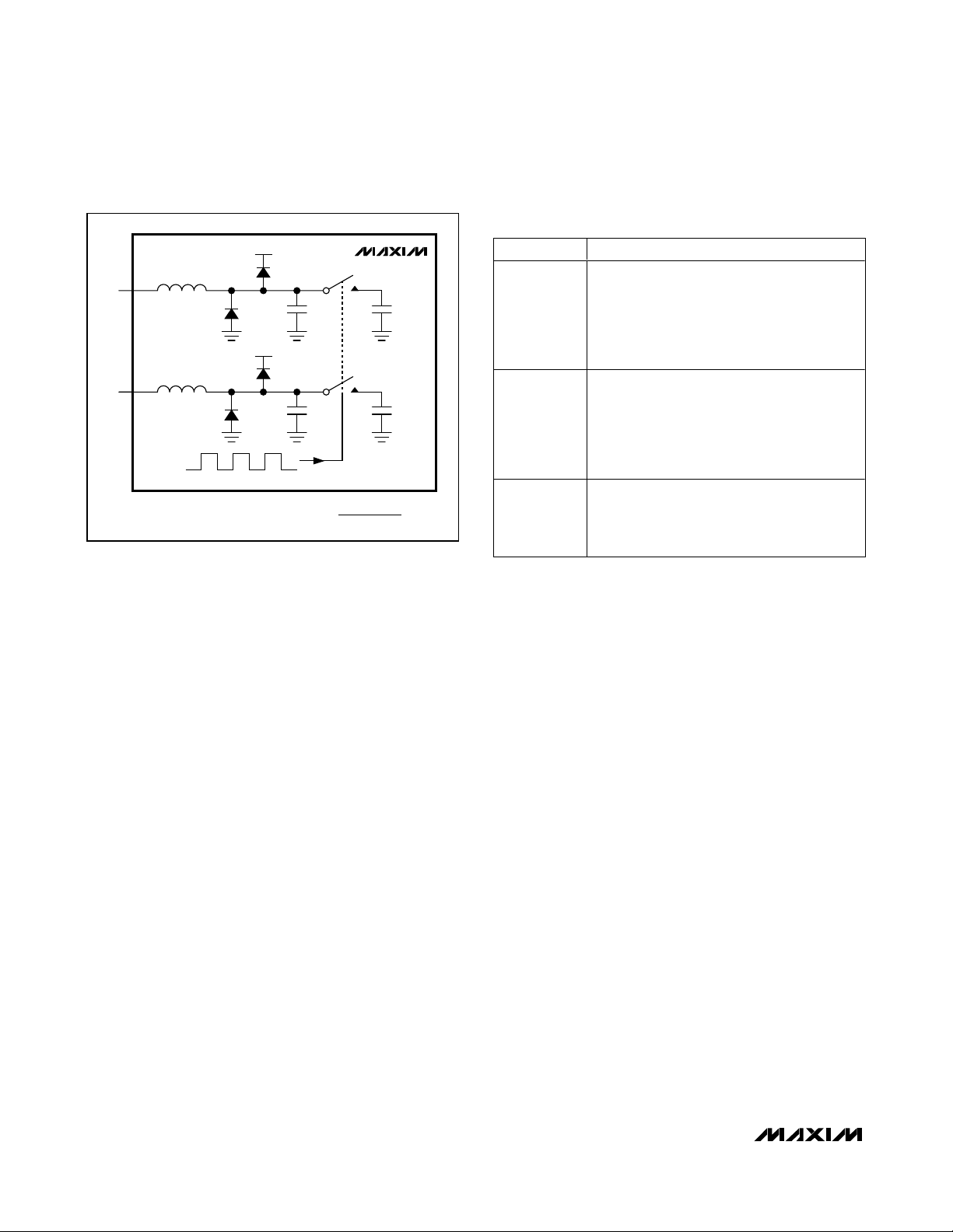
Detailed Description
The MAX12558 uses a 10-stage, fully differential,
pipelined architecture (Figure 1) that allows for highspeed conversion while minimizing power consumption. Samples taken at the inputs move progressively
through the pipeline stages every half clock cycle.
From input to output the total latency is 8 clock cycles.
Each pipeline converter stage converts its input voltage
to a digital output code. At every stage, except the last,
the error between the input voltage and the digital output code is multiplied and passed on to the next
pipeline stage. Digital error correction compensates for
ADC comparator offsets in each pipeline stage and
ensures no missing codes. Figure 2 shows the
MAX12558 functional diagram.
Dual, 80Msps, 14-Bit, IF/Baseband ADC
14 ______________________________________________________________________________________
Pin Description (continued)
Figure 1. Pipeline Architecture—Stage Blocks
PIN NAME FUNCTION
Power-Down Digital Input.
65 PD
66 SHREF
67 REFOUT
68 REFIN
—EP
PD = GND: ADCs are fully operational.
PD = OV
Shared Reference Digital Input.
SHREF = V
SHREF = GND: Shared reference disabled.
When sharing the reference, externally connect REFAP and REFBP together to ensure that V
V
REFBP
that V
Inter nal Refer ence V ol tag e O utp ut. The RE FOU T outp ut vol tag e i s 2.048V and RE FO U T can d el i ver 1m A.
For internal reference operation, connect REFOUT directly to REFIN or use a resistive divider from
REFOUT to set the voltage at REFIN. Bypass REFOUT to GND with a ≥ 0.1µF capacitor.
For external reference operation, REFOUT is not required and must be bypassed to GND with a ≥ 0.1µF
capacitor.
Single-Ended Reference Analog Input. For i nter nal r efer ence and b uffer ed exter nal r efer ence op er ati on,
ap p l y a 0.7V to 2.3V D C r efer ence vol tag e to RE FIN . B y p a s s REF I N t o GN D w it h a 4 . 7 µ F c a p a c i t o r .
W i thi n i ts sp eci fi ed op er ati ng vol tag e, RE FIN has a > 50M Ω i np ut i m p ed ance, and the d i ffer enti al
r efer ence vol tag e (
op er ati on, connect RE FIN to G N D . In thi s m od e, RE F_P , RE F_N , and C O M _ ar e hi g h- i m p ed ance i np uts
that accep t the exter nal r efer ence vol tag es.
Exposed Paddle. EP is internally connected to GND. Externally connect EP to GND to achieve the
specified dynamic performance.
: ADCs are powered down.
DD
: Shared reference enabled.
DD
. Similarly, when sharing the reference, externally connect REFAN to REFBN together to ensure
REFAN
= V
REFBN
V
R E F_ P
.
- V
) i s g ener ated fr om RE FIN . For unb uffer ed exter nal r efer ence
R E F_ N
REFAP
=
+
MAX12558
FLASH
ADC
IN_P
IN_N
STAGE 1 STAGE 9
STAGE 2
DIGITAL ERROR CORRECTION
Σ
DAC
D0_ THROUGH D13_
−
x2
STAGE 10
END OF PIPELINE

MAX12558
Dual, 80Msps, 14-Bit, IF/Baseband ADC
______________________________________________________________________________________ 15
Figure 2. Functional Diagram
CLOCK
INAP
INAN
REFAP
COMA
REFAN
REFIN
REFOUT
SHREF
REFBP
COMB
REFBN
INBP
INBN
DIFFCLK/SECLK
CLKP
CLKN
T/H
T/H
14-BIT
PIPELINE
ADC
CHANNEL A
REFERENCE
SYSTEM
CHANNEL B
REFERENCE
SYSTEM
14-BIT
PIPELINE
ADC
CLOCK
DIVIDER
DIGITAL
ERROR
CORRECTION
MAX12558
DIGITAL
ERROR
CORRECTION
DUTY-CYCLE
EQUALIZER
INTERNAL
REFERENCE
GENERATOR
CLOCK
CLOCK
DATA
FORMAT
DATA
FORMAT
OUTPUT
DRIVERS
OUTPUT
DRIVERS
POWER
CONTROL
AND
BIAS CIRCUITS
D0A TO D13A
DORA
G/T
DAV
OV
DD
D0B TO D13B
DORB
V
DD
PD
DIV2
DIV4
GND
MAX12558
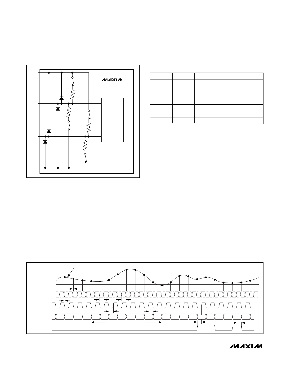
Analog Inputs and Input Track-and-Hold
(T/H) Amplifier
Figure 3 displays a simplified functional diagram of the
input T/H circuit. This input T/H circuit allows for high
analog input frequencies (high IF) of 175MHz and
beyond and supports a VDD/ 2 common-mode input
voltage.
The MAX12558 sampling clock controls the switchedcapacitor input T/H architecture (Figure 3) allowing the
analog input signals to be stored as charge on the
sampling capacitors. These switches are closed (track
mode) when the sampling clock is high and open (hold
mode) when the sampling clock is low (Figure 4). The
analog input signal source must be able to provide the
dynamic currents necessary to charge and discharge
the sampling capacitors. To avoid signal degradation,
these capacitors must be charged to one-half LSB
accuracy within one-half of a clock cycle. The analog
input of the MAX12558 supports differential or singleended input drive. For optimum performance with differential inputs, balance the input impedance of IN_P
and IN_N and set the common-mode voltage to midsupply (VDD/ 2). The MAX12558 provides the optimum
common-mode voltage of VDD/ 2 through the COM
output when operating in internal reference mode and
buffered external reference mode. This COM output
voltage can be used to bias the input network as shown
in Figures 9, 10, and 11.
Reference Output
An internal bandgap reference is the basis for all the
internal voltages and bias currents used in the
MAX12558. The power-down logic input (PD) enables
and disables the reference circuit. REFOUT has approximately 17kΩ to GND when the MAX12558 is powered
down. The reference circuit requires 10ms to power up
and settle to its final value when power is first applied to
the MAX12558 or when PD (power-down control line)
transitions from high to low.
The internal bandgap reference produces a buffered
reference voltage of 2.048V ±1% at the REFOUT pin
with a ±50ppm/°C temperature coefficient. Connect an
external ≥ 0.1µF bypass capacitor from REFOUT to
GND for stability. REFOUT sources up to 1mA and
sinks up to 0.1mA for external circuits with a 35mV/mA
load regulation. Short-circuit protection limits I
REFOUT
to a 2.1mA source current when shorted to GND and a
0.24mA sink current when shorted to VDD. Similar to
REFOUT, REFIN should be bypassed with a 4.7µF
capacitor to GND.
Reference Configurations
The MAX12558 full-scale analog input range is ±2/3 x
V
REF
with a VDD/ 2 ±0.5V common-mode input range.
V
REF
is the voltage difference between REFAP (REFBP)
and REFAN (REFBN). The MAX12558 provides three
modes of reference operation. Setting the voltage at
REFIN (V
REFIN
) selects the reference operation mode
(Table 1).
Dual, 80Msps, 14-Bit, IF/Baseband ADC
16 ______________________________________________________________________________________
Table 1. Reference Modes
Figure 3. Internal T/H Circuit
V
BOND WIRE
INDUCTANCE
IN_P
IN_N
1.5nH
BOND WIRE
INDUCTANCE
1.5nH
SAMPLING
CLOCK
*THE EFFECTIVE RESISTANCE OF THE
SWITCHED SAMPLING CAPACITORS IS:
DD
MAX12558
x C
1
SAMPLE
*C
4.5pF
*C
4.5pF
C
PAR
2pF
V
DD
C
PAR
2pF
RIN =
f
CLK
SAMPLE
SAMPLE
V
REFIN
Internal Reference Mode. REFIN is driven by
35% V
REFOUT
to 100%
V
REFOUT
0.7V to 2.3V
<0.5V
REFOUT either through a direct short or a
resistive divider.
V
COM_
V
REF_P
V
REF_N
Buffered External Reference Mode. An
external 0.7V to 2.3V reference voltage is
applied to REFIN.
V
COM_
V
REF_P
V
REF_N
U nb uffer ed E xter nal Refer ence M od e. RE F_P ,
RE F_N , and C O M _ ar e d r i ven b y exter nal
r efer ence sour ces. The ful l - scal e anal og i np ut
r ang e i s ± ( V
REFERENCE MODE
= VDD / 2
= VDD / 2 + 3/8 x V
= VDD / 2 - 3/8 x V
= VDD / 2
= VDD / 2 + 3/8 x V
= VDD / 2 - 3/8 x V
- V
R E F _P
R E F _N
REFIN
REFIN
REFIN
REFIN
) x 2/3.

Connect REFOUT to REFIN either with a direct short or
through a resistive divider for internal reference mode.
COM_, REF_P, and REF_N are low-impedance outputs
with V
COM_
= VDD/ 2, V
REFP
= VDD/ 2 + 3/8 x V
REFIN
,
and V
REF_N
= VDD/ 2 - 3/8 x V
REFIN
. Bypass REF_P,
REF_N, and COM_ each with a 0.1µF capacitor to GND.
Bypass REF_P to REF_N with a 10µF capacitor. Bypass
REFIN and REFOUT to GND with a 0.1µF capacitor. The
REFIN input impedance is very large (> 50MΩ). When
driving REFIN through a resistive divider, use resistances
≥ 10kΩ to avoid loading REFOUT.
Buffered external reference mode is virtually identical to
the internal reference mode except that the reference
source is derived from an external reference and not the
MAX12558’s internal bandgap reference. In buffered
external reference mode, apply a stable reference voltage source between 0.7V to 2.3V at REFIN. Pins COM_,
REF_P, and REF_N are low-impedance outputs with
V
COM_
= VDD/ 2, V
REF_P
= VDD/ 2 + 3/8 x V
REFIN
, and
V
REF_N
= VDD/ 2 - 3/8 x V
REFIN
. Bypass REF_P, REF_N,
and COM_ each with a 0.1µF capacitor to GND. Bypass
REF_P to REF_N with a 4.7µF capacitor.
Connect REFIN to GND to enter unbuffered external reference mode. Connecting REFIN to GND deactivates
the on-chip reference buffers for COM_, REF_P, and
REF_N. With their buffers deactivated, COM_, REF_P,
and REF_N become high-impedance inputs and must
be driven with separate, external reference sources.
Drive V
COM_
to VDD/ 2 ±5%, and drive REF_P and
REF_N so V
COM_
= (V
REF_P_
+ V
REF_N_
) / 2. The analog
input range is ±(V
REF_P_
- V
REF_N
) x 2/3. Bypass
REF_P, REF_N, and COM_ each with a 0.1µF capacitor
to GND. Bypass REF_P to REF_N with a 4.7µF capacitor.
For all reference modes, bypass REFOUT with a 0.1µF
and REFIN with a 4.7µF capacitor to GND.
The MAX12558 also features a shared reference mode,
in which the user can achieve better channel-to-channel matching. When sharing the reference (SHREF =
VDD), externally connect REFAP and REFBP together to
ensure that V
REFAP
= V
REFBP
. Similarly, when sharing
the reference, externally connect REFAN to REFBN
together to ensure that V
REFAN
= V
REFBN
.
Connect SHREF to GND to disable the shared reference mode of the MAX12558. In this independent reference mode, a better channel-to-channel isolation is
achieved.
For detailed circuit suggestions and how to drive the
ADC in buffered/unbuffered external reference mode,
see the Applications Information section.
Clock Duty-Cycle Equalizer
The MAX12558 has an internal clock duty-cycle equalizer, which makes the converter insensitive to the duty
cycle of the signal applied to CLKP and CLKN. The converters allow clock duty-cycle variations from 25% to 75%
without negatively impacting the dynamic performance.
The clock duty-cycle equalizer uses a delay-locked
loop (DLL) to create internal timing signals that are
duty-cycle independent. Due to this DLL, the
MAX12558 requires approximately 100 clock cycles to
acquire and lock to new clock frequencies.
Clock Input and Clock Control Lines
The MAX12558 accepts both differential and singleended clock inputs with a wide 25% to 75% input clock
duty cycle. For single-ended clock input operation,
connect DIFFCLK/SECLK and CLKN to GND. Apply an
external single-ended clock signal to CLKP. To reduce
clock jitter, the external single-ended clock must have
sharp falling edges. For differential clock input operation, connect DIFFCLK/SECLK to OV
DD
. Apply an
external differential clock signal to CLKP and CLKN.
Consider the clock input as an analog input and route it
away from any other analog inputs and digital signal
lines. CLKP and CLKN enter high impedance when the
MAX12558 is powered down (Figure 4).
Low clock jitter is required for the specified SNR performance of the MAX12558. The analog inputs are sampled on the falling (rising) edge of CLKP (CLKN),
requiring this edge to have the lowest possible jitter.
Jitter limits the maximum SNR performance of any ADC
according to the following relationship:
where f
IN
represents the analog input frequency and t
J
is the total system clock jitter. Clock jitter is especially
critical for undersampling applications. For instance,
assuming that clock jitter is the only noise source, to
obtain the specified 71.7dB of SNR with an input frequency of 175MHz the system must have less than
0.24ps of clock jitter. However, in reality there are other
noise sources such as thermal noise and quantization
noise that contribute to the system noise requiring the
clock jitter to be less than 0.17ps to obtain the specified 71.7dB of SNR at 175MHz.
Clock-Divider Control Inputs (DIV2, DIV4)
The MAX12558 features three different modes of sampling/clock operation (see Table 2). Pulling both control
lines low, the clock-divider function is disabled and the
converters sample at full clock speed. Pulling DIV4 low
MAX12558
Dual, 80Msps, 14-Bit, IF/Baseband ADC
______________________________________________________________________________________ 17
SNR
20
log
=×
⎛
⎜
2 π
⎝
1
ft
×× ×
IN J
⎞
⎟
⎠
MAX12558
and DIV2 high enables the divide-by-two feature, which
sets the sampling speed to one-half the selected clock
frequency. In divide-by-four mode, the converter sampling speed is set to one-fourth the clock speed of the
MAX12558. Divide-by-four mode is achieved by applying
a high level to DIV4 and a low level to DIV2. The option to
select either one-half or one-fourth of the clock speed for
sampling provides design flexibility, relaxes clock
requirements, and can minimize clock jitter.
System Timing Requirements
Figure 5 shows the timing relationship between the
clock, analog inputs, DAV indicator, DOR_ indicators,
and the resulting output data. The analog input is sam-
pled on the falling (rising) edge of CLKP (CLKN) and
the resulting data appears at the digital outputs 8 clock
cycles later.
The DAV indicator is synchronized with the digital output and optimized for use in latching data into digital
back-end circuitry. Alternatively, digital back-end circuitry can be latched with the rising edge of the conversion clock (CLKP - CLKN).
Data-Valid Output
DAV is a single-ended version of the input clock that is
compensated to correct for any input clock duty-cycle
variations. The MAX12558 output data changes on the
falling edge of DAV, and DAV rises once the output
data is valid. The falling edge of DAV is synchronized
to have a 5.4ns delay from the falling edge of the input
clock. Output data at D0A/B–D13A/B and DORA/B are
valid from 7ns before the rising edge of DAV to 7ns
after the rising edge of DAV.
DAV enters high impedance when the MAX12558 is
powered down (PD = OVDD). DAV enters its highimpedance state 10ns after the rising edge of PD and
becomes active again 10ns after PD transitions low.
DAV can sink and source 600µA and has three times the
driving capabilities of D0A/B–D13A/B and DORA/B. DAV
Dual, 80Msps, 14-Bit, IF/Baseband ADC
18 ______________________________________________________________________________________
Figure 4. Simplified Clock Input Circuit
Table 2. Clock-Divider Control Inputs
Figure 5. System Timing Diagram
V
DD
S
CLKP
S
1L
CLKN
GND
1H
Ω
10k
Ω
10k
S
2H
10k
SWITCHES S1_ AND S2_ ARE OPEN
DURING POWER-DOWN, MAKING
S
2L
CLKP AND CLKN HIGH IMPEDANCE.
SWITCHES S
SINGLE-ENDED CLOCK MODE.
10k
MAX12558
DUTY-CYCLE
EQUALIZER
Ω
Ω
ARE OPEN IN
2_
(V
(V
REF_P
REF_N
- V
REF_N
- V
REF_P
DAV
D0_–D13_
DOR
DIFFERENTIAL ANALOG INPUT (IN_P–IN_N)
) x 2/3
N - 3
N - 2
) x 2/3
CLKN
CLKP
t
DAV
t
N - 1
AD
N
N + 1
N + 3
N +2
t
CL
t
SETUP
8.0 CLOCK-CYCLE DATA LATENCY
N + 4
N + 5
t
CH
DIV4 DIV2 FUNCTION
00
01
10
1 1 Not Allowed
N + 6
t
HOLD
N + 7
N + 9
N + 8
N N + 1 N + 2 N + 3 N + 5 N + 6 N + 7N - 1N - 2N - 3 N + 9N + 8
Clock Divider Disabled
f
= f
SAMPLE
CLK
Divide-by-Two Clock Divider
f
= f
SAMPLE
CLK
/ 2
Divide-by-Four Clock Divider
= f
f
SAMPLE
CLK
/ 4
N + 4
t
SETUP
t
HOLD
is typically used to latch the MAX12558 output data into
an external digital back-end circuit. Keep the capacitive
load on DAV as low as possible (< 15pF) to avoid large
digital currents feeding back into the analog portion of
the MAX12558, thereby degrading its dynamic performance. Buffering DAV externally isolates it from heavy
capacitive loads. Refer to the MAX12558 EV kit schematic for recommendations of how to drive the DAV signal
through an external buffer.
Data Out-of-Range Indicator
The DORA and DORB digital outputs indicate when the
analog input voltage is out of range. When DOR_ is high,
the analog input is out of range. When DOR_ is low, the
analog input is within range. The valid differential input
range is from (V
REF_P
- V
REF_N
) x 2/3 to (V
REF_N
-
V
REF_P
) x 2/3. Signals outside of this valid differential
range cause DOR_ to assert high as shown in Table 1.
DOR is synchronized with DAV and transitions along
with the output data D13–D0. There is an 8 clock-cycle
latency in the DOR function as is with the output data
(Figure 5). DOR_ is high impedance when the
MAX12558 is in power-down (PD = high). DOR_ enters
a high-impedance state within 10ns after the rising edge
of PD and becomes active 10ns after PD’s falling edge.
Digital Output Data and Output Format Selection
The MAX12558 provides two 14-bit, parallel, tri-state
output buses. D0A/B–D13A/B and DORA/B update on
the falling edge of DAV and are valid on the rising edge
of DAV.
The MAX12558 output data format is either Gray code
or two’s complement depending on the logic input G/T.
With G/T high, the output data format is Gray code.
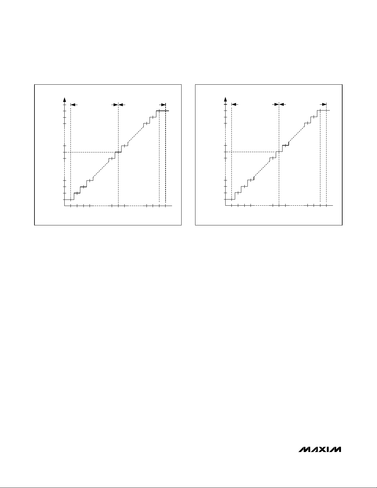
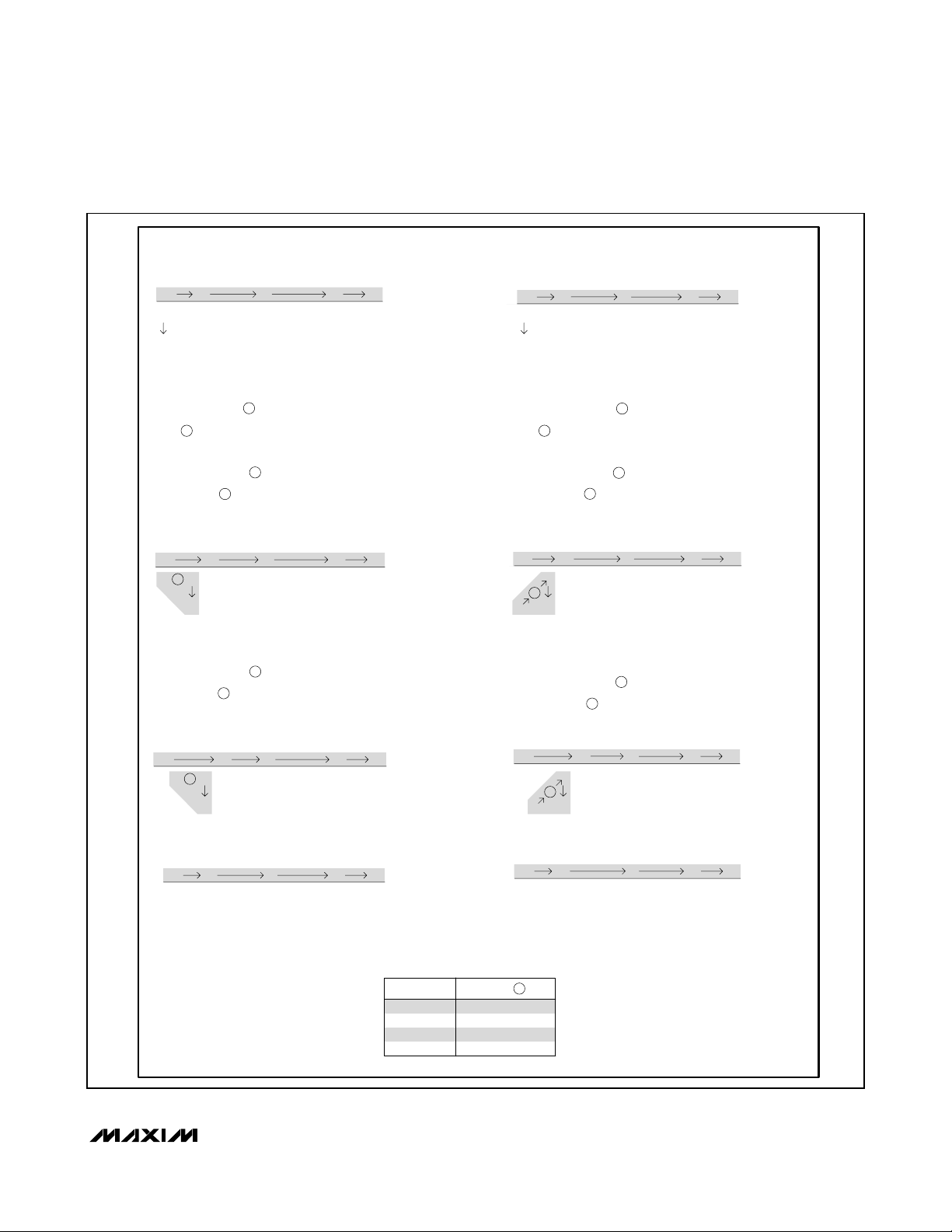
With G/T low, the output data format is set to two’s complement. See Figure 8 for a binary-to-Gray and Gray-tobinary code conversion example.
The following equations, Table 3, Figure 6, and Figure 7
define the relationship between the digital output and
the analog input.
Gray Code (G/T = 1):
V
IN_P
- V
IN_N
= 2/3 x (V
REF_P
- V
REF_N
) x 2 x
(CODE10- 8192) / 16,384
MAX12558
Dual, 80Msps, 14-Bit, IF/Baseband ADC
______________________________________________________________________________________ 19
Table 3. Output Codes vs. Input Voltage
GRAY-CODE OUTPUT CODE
(G/T = 1)
H EXA D ECIM A L
BINARY
D13A–D0A
D13B–D0B
10 0000 0000 0000 1 0x2000 +16,383 01 1111 1111 1111 1 0x1FFF +8191
10 0000 0000 0000 0 0x2000 +16,383 01 1111 1111 1111 0 0x1FFF +8191 +1.023875V
10 0000 0000 0001 0 0x2001 +16,382 01 1111 1111 1110 0 0x1FFE +8190 +1.023750V
DOR
EQUIVALENT
OF
D13A–D0A
D13B–D0B
DECIMAL
EQUIVALENT
OF
D13A–D0A
D13B–D0B
(CODE
)
10
TWO’S-COMPLEMENT OUTPUT CODE
(G/T = 0)
HEXADECIMAL
BINARY
D13A–D0A
D13B–D0B
DOR
EQUIVALENT
OF
D13A–D0A
D13B–D0B
DECIMAL
EQUIVALENT
OF
D13A–D0A
D13B–D0B
(CODE10)
- V
V
IN_P
V
= 2.418V
REF_P
V
= 0.882V
REF_N
> +1.023875V
(DATA OUT OF
RANGE)
IN_N
11 0000 0000 0011 0 0x3003 +8194 00 0000 0000 0010 0 0x0002 +2 +0.000250V
11 0000 0000 0001 0 0x3001 +8193 00 0000 0000 0001 0 0x0001 +1 +0.000125V
11 0000 0000 0000 0 0x3000 +8192 00 0000 0000 0000 0 0x0000 0 +0.000000V
01 0000 0000 0000 0 0x1000 +8191 11 1111 1111 1111 0 0x3FFF -1 -0.000125V
01 0000 0000 0001 0 0x1001 +8190 11 1111 1111 1110 0 0x3FFE -2 -0.000250V
00 0000 0000 0001 0 0x0001 +1 10 0000 0000 0001 0 0x2001 -8191 -1.023875V
00 0000 0000 0000 0 0x0000 0 10 0000 0000 0000 0 0x2000 -8192 -1.024000V
< -1.024000V
00 0000 0000 0000 1 0x0000 0 10 0000 0000 0000 1 0x2000 -8192
(DATA OUT OF
RANGE)
MAX12558
Two’s Complement (G/T = 0):
V
IN_P
- V
IN_N
= 2/3 x (V
REF_P
- V
REF_N
) x 2 x
CODE10/ 16,384
where CODE10is the decimal equivalent of the digital
output code as shown in Table 3.
The digital outputs D0A/B–D13A/B are high impedance
when the MAX12558 is in power-down (PD = 1) mode.
D0A/B–D13A/B enter this state 10ns after the rising
edge of PD and become active again 10ns after PD
transitions low.
Keep the capacitive load on the MAX12558 digital outputs D0A/B–D13A/B as low as possible (< 15pF) to
avoid large digital currents feeding back into the analog portion of the converter and degrading its dynamic
performance. Adding external digital buffers on the digital outputs helps isolate the MAX12558 from heavy
capacitive loads. To improve the dynamic performance
of the MAX12558, add 220Ω resistors in series with the
digital outputs close to the MAX12558. Refer to the
MAX12558 EV kit schematic for guidelines of how to
drive the digital outputs through 220Ω series resistors
and external digital output buffers.
Power-Down Input
The MAX12558 has two power modes that are controlled with a power-down digital input (PD). With PD
low, the converter is in its normal operating mode. With
PD high, the MAX12558 is in power-down mode.
The power-down mode allows the MAX12558 to efficiently use power by transitioning to a low-power state
when conversions are not required. Additionally, the
MAX12558 parallel output bus goes high impedance in
power-down mode, allowing other devices on the bus
to be accessed.
In power-down mode all internal circuits are off, the
analog supply current reduces to less than 50µA, and
the digital supply current reduces to 1µA. The following
list shows the state of the analog inputs and digital outputs in power-down mode.
1) INAP/B, INAN/B analog inputs are disconnected
from the internal input amplifier (Figure 3).
2) REFOUT has approximately 17kΩ to GND.
3) REFAP/B, COMA/B, REFAN/B enter a high-impedance state with respect to V
DD
and GND, but there
is an internal 4kΩ resistor between REFAP/B and
COMA/B as well as an internal 4kΩ resistor
between REFAN/B and COMA/B.
4) D0A–D13A, D0B–D13B, DORA, and DORB enter a
high-impedance state.
5) DAV enters a high-impedance state.
6) CLKP, CLKN clock inputs enter a high-impedance
state (Figure 4).
Dual, 80Msps, 14-Bit, IF/Baseband ADC
20 ______________________________________________________________________________________
Figure 6. Two’s-Complement Transfer Function (G/T= 0)
Figure 7. Gray-Code Transfer Function (G/T= 1)
2/3 x (V
0x1FFF
0x1FFE
0x1FFD
0x0001
0x0000
0x3FFF
0x2003
TWO'S-COMPLEMENT OUTPUT CODE (LSB)
0x2002
0x2001
0x2000
-8189 +8191+8189-1 0 +1-8191
1 LSB = 4/3 x (V
- V
REFP
DIFFERENTIAL INPUT VOLTAGE (LSB)
REFP
) 2/3 x (V
REFN
- V
REFN
) / 16,384
REFP
- V
REFN
)
0x2000
0x2001
0x2003
0x3001
0x3000
0x1000
GRAY OUTPUT CODE (LSB)
0x0002
0x0003
0x0001
0x0000
1 LSB = 4/3 x (V
- V
2/3 x (V
REFP
-8189 +8191+8189-1 0 +1-8191
DIFFERENTIAL INPUT VOLTAGE (LSB)
REFP
) 2/3 x (V
REFN
- V
REFN
) / 16,384
REFP
- V
REFN
)
MAX12558
Dual, 80Msps, 14-Bit, IF/Baseband ADC
______________________________________________________________________________________ 21
Figure 8. Binary-to-Gray and Gray-to-Binary Code Conversion
BINARY-TO-GRAY CODE CONVERSION
1) THE MOST SIGNIFICANT GRAY-CODE BIT IS THE SAME
AS THE MOST SIGNIFICANT BINARY BIT.
D13 D7 D3 D0
D11
01 10 0100 1100 BINARY
11
BIT POSITION
GRAY-TO-BINARY CODE CONVERSION
1) THE MOST SIGNIFICANT BINARY BIT IS THE SAME AS THE
MOST SIGNIFICANT GRAY-CODE BIT.
D13 D7 D3 D0
D11
11
BIT POSITION
GRAY CODE01 0 0 11 011010
GRAY CODE0
2) SUBSEQUENT GRAY-CODE BITS ARE FOUND ACCORDING
TO THE FOLLOWING EQUATION:
GRAYX = BINARYX +BINARY
+
WHERE IS THE EXCLUSIVE OR FUNCTION (SEE TRUTH
TABLE BELOW) AND X IS THE BIT POSITION:
GRAY
= BINARY12BINARY
12
+
GRAY12 = 1 0
GRAY
= 1
12
D13 D7 D3 D0
D11
+
0 110 0100 1100 BINARY
3) REPEAT STEP 2 UNTIL COMPLETE:
GRAY
GRAY11 = 1 1
GRAY
D13 D7 D3 D0
01 10 0100 1100 BINARY
10
11
1
= BINARY11BINARY
11
+
= 0
11
D11
11
+
+
+
X + 1
13
BIT POSITION
GRAY CODE0
12
BIT POSITION
GRAY CODE0
0 BINARY
2) SUBSEQUENT BINARY BITS ARE FOUND ACCORDING TO
THE FOLLOWING EQUATION:
X+1
+
10
+
= 1
D11
110
+
GRAY
X
+
12
+
11
= BINARY
BINARY
X
+
WHERE IS THE EXCLUSIVE OR FUNCTION (SEE TRUTH
TABLE BELOW) AND X IS THE BIT POSITION:
= BINARY13GRAY
BINARY
12
BINARY12 = 0 1
BINARY
= 1
12
D13 D7 D3 D0
D11
0 101 1110 1010
+
0
1
3) REPEAT STEP 2 UNTIL COMPLETE:
= BINARY12GRAY
BINARY
11
BINARY11 = 1 0
BINARY
11
D13 D7 D3 D0
01 0 1110 1010
+
0
11
BIT POSITION
GRAY CODE
BINARY
BIT POSITION
GRAY CODE
BINARY
4) THE FINAL GRAY-CODE CONVERSION IS:
D13 D7 D3 D0
D11
01 10 0100 1100 BINARY
101 11 01 1010
FIGURE 8 SHOWS THE GRAY-TO-BINARY AND BINARY-TO-GRAY
CODE CONVERSION IN OFFSET BINARY FORMAT. THE OUTPUT
FORMAT OF THE MAX12558 IS TWO'S-COMPLEMENT BINARY,
HENCE EACH MSB OF THE TWO'S-COMPLEMENT OUTPUT CODE
MUST BE INVERTED TO REFLECT TRUE OFFSET BINARY FORMAT.
11
10
BIT POSITION
GRAY CODE0
EXCLUSIVE OR TRUTH TABLE
AB Y=AB
00
01
10
11
4) THE FINAL BINARY CONVERSION IS:
D13 D7 D3 D0
D11
01 0 0 1110 1010
01 1 1 0100 1100
+
0
1
1
0
11
01
BIT POSITION
GRAY CODE
BINARY
MAX12558
The wake-up time from power-down mode is dominated
by the time required to charge the capacitors at REF_P,
REF_N, and COM_. In internal reference mode and
buffered external reference mode the wake-up time is
typically 10ms. When operating in the unbuffered external reference mode the wake-up time is dependent on
the external reference drivers.
Applications Information
Using Transformer Coupling
In general, the MAX12558 provides better SFDR and
THD with fully differential input signals than singleended input drive, especially for input frequencies
above 125MHz. In differential input mode, even-order
harmonics are lower as both inputs are balanced, and
each of the ADC inputs only requires half the signal
swing compared to single-ended input mode.
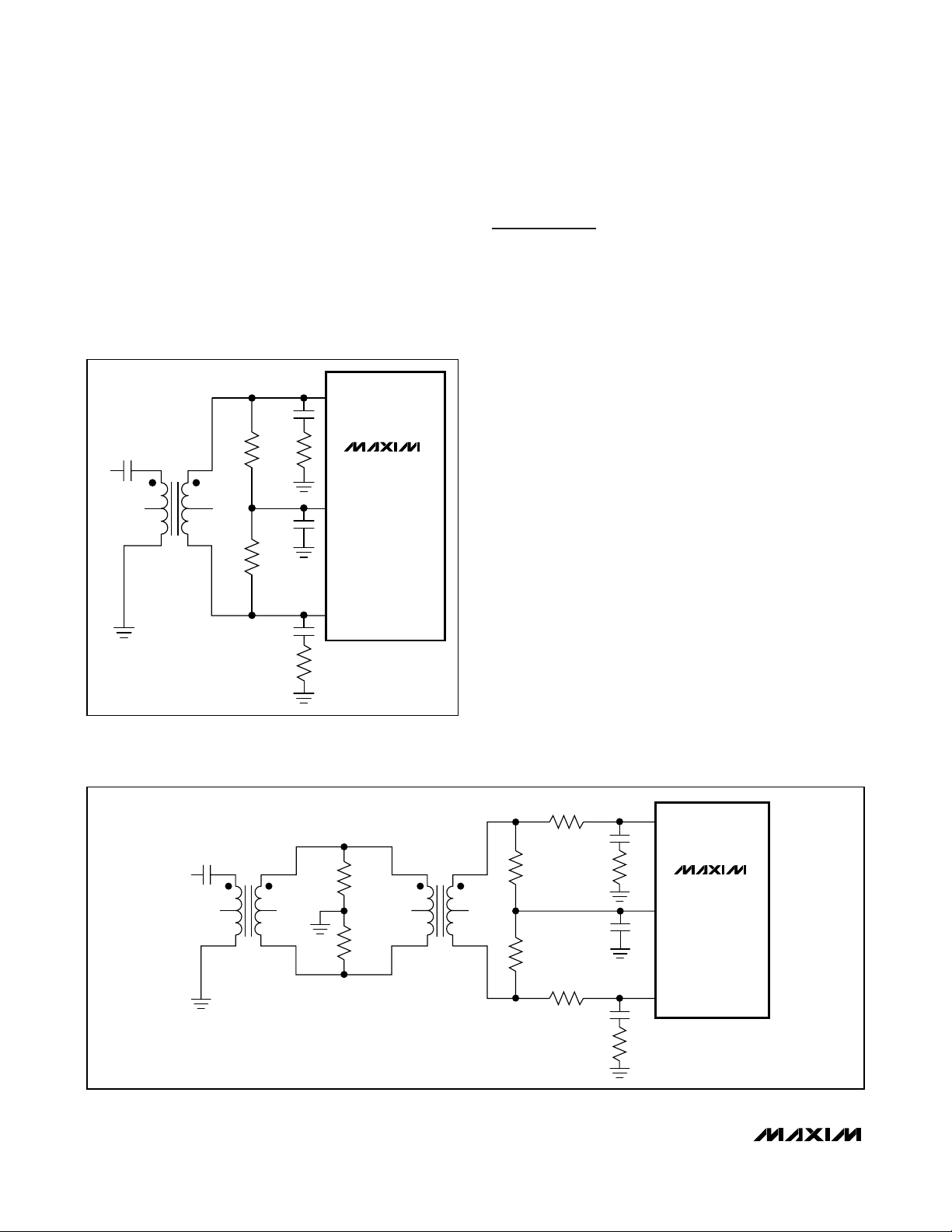
An RF transformer (Figure 9) provides an excellent
solution to convert a single-ended input source signal
to a fully differential signal, required by the MAX12558
for optimum performance. Connecting the center tap of
the transformer to COM provides a VDD/ 2 DC level
shift to the input. Although a 1:1 transformer is shown, a
step-up transformer can be selected to reduce the
drive requirements. A reduced signal swing from the
input driver, such as an op amp, can also improve the
overall distortion. The configuration of Figure 9 is good
for frequencies up to Nyquist (f
CLK
/ 2).
The circuit of Figure 10 converts a single-ended input
signal to fully differential just as Figure 9. However,
Figure 10 utilizes an additional transformer to improve
the common-mode rejection allowing high-frequency
signals beyond the Nyquist frequency. A set of 75Ω
and 110Ω termination resistors provide an equivalent
50Ω termination to the signal source. The second set of
termination resistors connects to COM_ providing the
correct input common-mode voltage. Two 0Ω resistors
in series with the analog inputs allow high-IF input frequencies. These 0Ω resistors can be replaced with lowvalue resistors to limit the input bandwidth.
Dual, 80Msps, 14-Bit, IF/Baseband ADC
Figure 9. Transformer-Coupled Input Drive for Input Frequencies
Up to Nyquist
Figure 10. Transformer-Coupled Input Drive for Input Frequencies Beyond Nyquist
22 ______________________________________________________________________________________
5.6pF
49.9Ω
0.1µF
V
IN
1
5
N.C. N.C.
3
MINI-CIRCUITS
ADT1-1WT
T1
0.5%
6
2
4
49.9Ω
0.5%
24.9Ω
0.1µF
5.6pF
24.9Ω
IN_P
MAX12558
COM_
IN_N
V
IN
0.1µF
N.C.
1
6
T1
5
2
3
4
MINI-CIRCUITS
ADT1-1WT
N.C.
0Ω*
Ω
1
Ω
75
0.5%
N.C.
Ω
75
0.5%
*0Ω RESISTORS CAN BE REPLACED WITH
LOW-VALUE RESISTORS TO LIMIT THE INPUT BANDWIDTH.
MINI-CIRCUITS
T2
5
3
ADT1-1WT
6
2
N.C.
4
110
0.5%
110
0.5%
Ω
0Ω*
C
0.1µF
C
IN
R
IN
IN
R
IN
IN_P
MAX12558
COM_
IN_N
The input network in Figure 10 can be modified to enhance
the frequency-range-specific AC performance of the
MAX12558 by simply replacing the input capacitance with
a series network of resistor (RIN) and capacitor (CIN).
Table 4 displays a selection of resistors and capacitors
that are recommended to help improve the already
excellent performance of this ADC for specific applications requiring only a certain range of input frequencies.
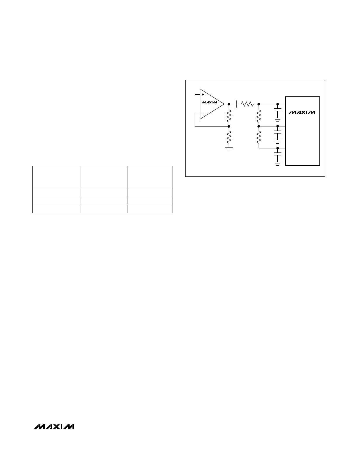
Single-Ended AC-Coupled Input Signal
Figure 11 shows an AC-coupled, single-ended input
application. The MAX4108 provides high speed, high
bandwidth, low noise, and low distortion to maintain the
input signal integrity.
Buffered External Reference Drives
Multiple ADCs
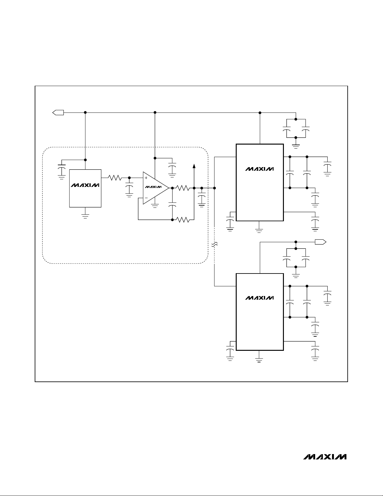
The buffered external reference mode allows for more
control over the MAX12558 reference voltage and
allows multiple converters to use a common reference.
The REFIN input impedance is > 50MΩ.
Figure 12 shows the MAX6029 precision 2.048V bandgap
reference used as a common reference for multiple converters. The 2.048V output of the MAX6029 passes
through a single-pole 10Hz LP filter to the MAX4230.
The MAX4250 buffers the 2.048V reference and provides additional 10Hz LP filtering before its output is
applied to the REFIN input of the MAX12558.
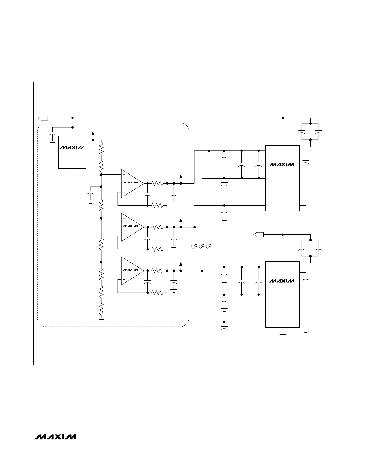
Unbuffered External Reference Drives
Multiple ADCs
The unbuffered external reference mode allows for precise control over the MAX12558 reference and allows
multiple converters to use a common reference.
Connecting REFIN to GND disables the internal reference, allowing REF_P, REF_N, and COM_ to be driven
directly by a set of external reference sources.
Figure 13 uses a MAX6029 precision 3.000V bandgap
reference as a common reference for multiple converters. A seven-component resistive divider chain follows
the MAX6029 voltage reference. The 0.47µF capacitor
along this chain creates a 10Hz LP filter. Three
MAX4230 amplifiers buffer taps along this resistor
chain providing 2.413V, 1.647V, and 0.880V to the
MAX12558 REF_P, REF_N, and COM_ reference inputs.
The feedback around the MAX4230 op amps provides
additional 10Hz LP filtering. Reference voltages 2.413V
and 0.880V set the full-scale analog input range for the
converter to ±1.022V (±[V
REF_P
- V
REF_N
] x 2/3).
Note that one single power supply for all active circuit
components removes any concern regarding powersupply sequencing when powering up or down.
MAX12558
Dual, 80Msps, 14-Bit, IF/Baseband ADC
______________________________________________________________________________________ 23
Figure 11. Single-Ended, AC-Coupled Input Drive
Table 4. Component Selection to
Enhance the Frequency-Range-Specific
AC Performance
INPUT
FREQUENCY
RANGE
< 10MHz 12pF to 22pF 0Ω
10MHz to 125MHz 12pF 50Ω
> 125MHz 5.6pF 0Ω
C
IN
COMPONENT
VALUES
R
IN
COMPONENT
VALUES
V
IN
MAX4108
100Ω
100Ω
0.1µF
0Ω
24.9Ω
24.9Ω
IN_P
5.6pF
MAX12558
COM_
0.1µF
IN_N
5.6pF
MAX12558
Dual, 80Msps, 14-Bit, IF/Baseband ADC
24 ______________________________________________________________________________________
Figure 12. External Buffered (MAX4230) Reference Drive Using a MAX6029 Bandgap Reference
3.3V
0.1µF
NOTE: ONE FRONT-END REFERENCE CIRCUIT
CAN SOURCE UP TO 15mA AND SINK UP TO
30mA OF OUTPUT CURRENT.
1
MAX6029
(EUK21)
2
0.1µF
V
DD
GND
V
REF_P
REF_N
COM_
0.1µF
DD
REF_P
2.048V
0.1µF
16.2kΩ
5
1µF
3
4
MAX4230
5
1
2
47Ω
1.47kΩ
300µF
6V
0.1µF
REFIN
MAX12558
REFOUT
REFIN
MAX12558
10µF
10µF
2.2µF
0.1µF
0.1µF
0.1µF
0.1µF
3.3V
2.2µF
0.1µF
0.1µF
REF_N
0.1µF
REFOUT
COM_
GND
0.1µF
0.1µF
MAX12558
Dual, 80Msps, 14-Bit, IF/Baseband ADC
______________________________________________________________________________________ 25
3.3V
Figure 13. External Unbuffered Reference Driving Multiple ADCs
0.1µF
1
MAX6029
(EUK30)
2
0.47µF
3V
5
20kΩ
1%
20kΩ
1%
52.3kΩ
1%
52.3kΩ
1%
20kΩ
1%
20kΩ
1%
20kΩ
1%
0.1µF
10µF
0.1µF
1
47Ω
10µF
10µF
10µF
4
6V
1.47kΩ
47Ω
4
6V
1.47kΩ
47Ω
4
6V
1.47kΩ
MAX4230
3
1
MAX4230
3
1
MAX4230
3
2.413V
0.1µF
330µF
6V
1.647V
330µF
6V
0.880V
330µF
6V
0.1µF
0.1µF
0.1µF
0.1µF
10µF
0.1µF
REF_P
REF_N
COM_
3.3V
REF_P
REF_N
COM_
V
DD
MAX12558
GND
V
DD
MAX12558
GND
0.1µF
REFOUT
REFIN
0.1µF
REFOUT
REFIN
2.2µF
0.1µF
2.2µF
0.1µF

MAX12558
Dual, 80Msps, 14-Bit, IF/Baseband ADC
26 ______________________________________________________________________________________
Grounding, Bypassing, and
Board Layout
The MAX12558 requires high-speed board layout
design techniques. Refer to the MAX12558 EV kit data
sheet for a board layout reference. Locate all bypass
capacitors as close to the device as possible, preferably on the same side as the ADC, using surfacemount devices for minimum inductance. Bypass VDDto
GND with a 220µF ceramic capacitor in parallel with at
least one 10µF, one 4.7µF, and one 0.1µF ceramic
capacitor. Bypass OV
DD
to GND with a 220µF ceramic
capacitor in parallel with at least one 10µF, one 4.7µF,
and one 0.1µF ceramic capacitor. High-frequency
bypassing/decoupling capacitors should be located as
close as possible to the converter supply pins.
Multilayer boards with ample ground and power planes
produce the highest level of signal integrity. All grounds
and the exposed backside paddle of the MAX12558
must be connected to the same ground plane. The
MAX12558 relies on the exposed backside paddle connection for a low-inductance ground connection. Isolate
the ground plane from any noisy digital system ground
planes such as a DSP or output buffer ground.
Route high-speed digital signal traces away from the
sensitive analog traces. Keep all signal lines short and
free of 90° turns.
Ensure that the differential, analog input network layout
is symmetric and that all parasitic components are balanced equally. Refer to the MAX12558 EV kit data
sheet for an example of symmetric input layout.
Parameter Definitions
Integral Nonlinearity (INL)
INL is the deviation of the values on an actual transfer
function from a straight line. For the MAX12558, this
straight line is between the endpoints of the transfer
function, once offset and gain errors have been nullified.
INL deviations are measured at every step of the transfer
function and the worst-case deviation is reported in the
Electrical Characteristics table.
Differential Nonlinearity (DNL)
DNL is the difference between an actual step width and
the ideal value of 1 LSB. A DNL error specification of
less than 1 LSB guarantees no missing codes and a
monotonic transfer function. For the MAX12558, DNL
deviations are measured at every step of the transfer
function and the worst-case deviation is reported in the
Electrical Characteristics table.
Offset Error
Offset error is a figure of merit that indicates how well
the actual transfer function matches the ideal transfer
function at a single point. Ideally the midscale
MAX12558 transition occurs at 0.5 LSB above midscale. The offset error is the amount of deviation
between the measured midscale transition point and
the ideal midscale transition point.
Gain Error
Gain error is a figure of merit that indicates how well the
slope of the actual transfer function matches the slope of
the ideal transfer function. The slope of the actual transfer
function is measured between two data points: positive
full scale and negative full scale. Ideally, the positive fullscale MAX12558 transition occurs at 1.5 LSBs below positive full scale, and the negative full-scale transition
occurs at 0.5 LSB above negative full scale. The gain
error is the difference of the measured transition points
minus the difference of the ideal transition points.
Small-Signal Noise Floor (SSNF)
SSNF is the integrated noise and distortion power in the
Nyquist band for small-signal inputs. The DC offset is
excluded from this noise calculation. For this converter,
a small signal is defined as a single tone with a -35dBFS
amplitude. This parameter captures the thermal and
quantization noise characteristics of the data converter
and can be used to help calculate the overall noise figure of a digital receiver signal path.
Signal-to-Noise Ratio (SNR)
For a waveform perfectly reconstructed from digital
samples, the theoretical maximum SNR is the ratio of
the full-scale analog input (RMS value) to the RMS
quantization error (residual error). The ideal, theoretical
minimum analog-to-digital noise is caused by quantization error only and results directly from the ADC’s resolution (N bits):
SNR
[max]
= 6.02 × N + 1.76
In reality, there are other noise sources besides quantization noise: thermal noise, reference noise, clock jitter,
etc. SNR is computed by taking the ratio of the RMS
signal to the RMS noise. RMS noise includes all spectral components to the Nyquist frequency excluding the
fundamental, the first six harmonics (HD2 through
HD7), and the DC offset.
SNR = 20 x log (SIGNAL
RMS
/ NOISE
RMS
)

Signal-to-Noise Plus Distortion (SINAD)
SINAD is computed by taking the ratio of the RMS signal to the RMS noise plus distortion. RMS noise plus
distortion includes all spectral components to the
Nyquist frequency excluding the fundamental and the
DC offset.
Total Harmonic Distortion (THD)
THD is the ratio of the RMS sum of the first six harmonics of the input signal to the fundamental itself. This is
expressed as:
where V1is the fundamental amplitude, and V2through
V7are the amplitudes of the 2nd- through 7th-order
harmonics (HD2 through HD7).
Spurious-Free Dynamic Range (SFDR)
SFDR is the ratio expressed in decibels of the RMS
amplitude of the fundamental (maximum signal component) to the RMS value of the next largest spurious
component, excluding DC offset.
3rd-Order Intermodulation (IM3)
IM3 is the power of the 3rd-order intermodulation product relative to the input power of either of the input tones
f
IN1
and f
IN2
. The individual input tone power levels are
set to -7dBFS for the MAX12558. The 3rd-order intermodulation products are 2 x f
IN1
- f
IN2
and 2 x f
IN2
- f
IN1
.
Aperture Jitter
Figure 14 shows the aperture jitter (tAJ), which is the
sample-to-sample variation in the aperture delay.
Aperture Delay
Aperture delay (tAD) is the time defined between the
rising edge of the sampling clock and the instant when
an actual sample is taken (Figure 14).
Full-Power Bandwidth
A large -0.2dBFS analog input signal is applied to an
ADC and the input frequency is swept up to the point
where the amplitude of the digitized conversion result
has decreased by -3dB. This point is defined as the
full-power input bandwidth frequency.
Output Noise (n
OUT
)
The output noise (n
OUT
) parameter is similar to thermal
plus quantization noise and is an indication of the converter’s overall noise performance.
No fundamental input tone is used to test for n
OUT
.
IN_P, IN_N, and COM_ are connected together and
1024k data points are collected. n
OUT
is computed by
taking the RMS value of the collected data points after
the mean is removed.
Overdrive Recovery Time
Overdrive recovery time is the time required for the
ADC to recover from an input transient that exceeds the
full-scale limits. The MAX12558 specifies overdrive
recovery time using an input transient that exceeds the
full-scale limits by ±10%. The MAX12558 requires one
clock cycle to recover from the overdrive condition.
Crosstalk
Crosstalk indicates how well each channel is isolated
from the other channel. In case of the MAX12558,
crosstalk specifies the coupling onto one channel
being driven by a (-0.5dBFS) signal when the adjacent
interfering channel is driven by a full-scale signal.
Measurement includes all spurs resulting from both
direct coupling and mixing components.
Gain Matching
Gain matching is a figure of merit that indicates how
well the gains between the two channels are matched
to each other. The same input signal is applied to both
channels and the maximum deviation in gain is reported (typically in dB) as gain matching.
Offset Matching
Like gain matching, offset matching is a figure of merit
that indicates how well the offsets between the two channels are matched to each other. The same input signal is
applied to both channels and the maximum deviation in
offset is reported (typically in %FSR) as offset matching.
MAX12558
Dual, 80Msps, 14-Bit, IF/Baseband ADC
______________________________________________________________________________________ 27
Figure 14. T/H Aperture Timing
THD
log
=×
20
⎛
2
2
2
2
VVVVVV
+++++
2
3
⎜
⎜
⎝
4
V
1
2
5
6
⎞
2
7
⎟
⎟
⎠
CLKN
CLKP
ANALOG
INPUT
SAMPLED
DATA
T/H
TRACKHOLD HOLD
t
AD
t
AJ

MAX12558
Dual, 80Msps, 14-Bit, IF/Baseband ADC
28 ______________________________________________________________________________________
MAX12558
4142434445 3738394046
21
22
23
24
25
26
27
28
29
30
THIN QFN
TOP VIEW
3536
D2B
D1B
D0B
OV
DD
V
DD
V
DD
V
DD
V
DD
DIV4
DIV2
18
19
20
CLKP
CLKN
DIFFCLK/SECLK
EXPOSED PADDLE (GND)
31 D3B
4748495051
654321098711211 151413 1716
32
33
D5B
D4B
34 D6B
D2A
D1A
D0A
DAV
OV
DD
DORB
D13B
D12B
D11B
D10B
D9B
D8B
D7B
D3A
D5A
D4A
D6A
62
61
60
59
58
57
56
55
54
53
67
66
65
64
63
52
68
REFBP
REFBN
GND
REFAN
REFAP
COMA
INBP
INBN
GND
GND
COMB
GND
GND
INAN
INAP
GND
GND
MAX12558
D12A
D13A
DORA
OV
DD
V
DD
V
DD
V
DD
G/T
PD
SHREF
REFOUT
REFIN
D11A
D8A
D9A
D10A
D7A
Pin Configuration

MAX12558
Dual, 80Msps, 14-Bit, IF/Baseband ADC
______________________________________________________________________________________ 29
Package Information
(The package drawing(s) in this data sheet may not reflect the most current specifications. For the latest package outline information,
go to www.maxim-ic.com/packages
.)
68L QFN THIN.EPS
PACKAGE OUTLINE
68L THIN QFN, 10x10x0.8mm
21-0142
1
D
2

MAX12558
Dual, 80Msps, 14-Bit, IF/Baseband ADC
Maxim cannot assume responsibility for use of any circuitry other than circuitry entirely embodied in a Maxim product. No circuit patent licenses are
implied. Maxim reserves the right to change the circuitry and specifications without notice at any time.
30 ____________________Maxim Integrated Products, 120 San Gabriel Drive, Sunnyvale, CA 94086 408-737-7600
© 2004 Maxim Integrated Products Printed USA is a registered trademark of Maxim Integrated Products, Inc.
Heaney
Package Information (continued)
(The package drawing(s) in this data sheet may not reflect the most current specifications. For the latest package outline information,
go to www.maxim-ic.com/packages
.)
MAX12558
PACKAGE OUTLINE
68L THIN QFN, 10x10x0.8mm
21-0142
2
D
2
 Loading...