

Page 1
General Description
The MAX1253/MAX1254 are stand-alone, 10-channel (8
external, 2 internal) 12-bit system monitor ADCs with
internal reference. A programmable single-ended/differential mux accepts voltage and remote-diode temperature-sensor inputs. These devices independently
monitor the input channels without microprocessor
interaction and generate an interrupt when any variable
exceeds user-defined limits. The MAX1253/MAX1254
configure both high and low limits, as well as the number of fault cycles allowed, before generating an interrupt. These ADCs can also perform recursive data
averaging for noise reduction. Programmable wait intervals between conversion sequences allow the selection
of the sample rate.
At the maximum sampling rate of 94ksps (auto mode,
single channel enabled), the MAX1253 consumes only
5mW (1.7mA at 3V). AutoShutdownTMreduces supply
current to 190µA at 2ksps and to less than 8µA at 50sps.
Stand-alone operation, combined with ease of use in a
small package (16-pin TSSOP), makes the MAX1253/
MAX1254 ideal for multichannel system-monitoring
applications. Low power consumption also makes
these devices a good fit for hand-held and battery-powered applications.
Applications
System Supervision
Remote Telecom Networks
Server Farms
Remote Data Loggers
Features
♦ Monitor 10 Signals Without Processor
Intervention
♦ Eight External Channels Programmable as
Temperature or Voltage Monitors
♦ Intelligent Circuitry for Reliable Autonomous
Measurement
Programmable Digital Averaging Filter
Programmable Fault Counter
♦ Precision Measurements
12-Bit Resolution
±1 LSB INL, ±1 LSB DNL
±0.75°C Temperature Accuracy (typ)
♦ Flexible
Automatic Channel Scan Sequencer with
Programmable Intervals
Programmable Inputs: Single Ended/Differential,
Voltage/Temperature
Programmable Wait State
♦ Internal 2.5V/4.096V Reference
(MAX1253/MAX1254)
♦ Remote Temperature Sensing Up to 10m
(Differential Mode)
♦ Single 3V or 5V Supply Operation
♦ Small 16-Pin TSSOP Package
MAX1253/MAX1254
Stand-Alone, 10-Channel, 12-Bit System Monitors
with Internal Temperature Sensor and V
DD
Monitor
________________________________________________________________ Maxim Integrated Products 1
Selector Guide
19-2838; Rev 0; 4/03
For pricing, delivery, and ordering information, please contact Maxim/Dallas Direct! at
1-888-629-4642, or visit Maxim’s website at www.maxim-ic.com.
*Future product—contact factory for availability.
*Future product—contact factory for availability.
Typical Application Circuit appears at end of data sheet.
AutoShutdown is a trademark of Maxim Integrated Products, Inc.
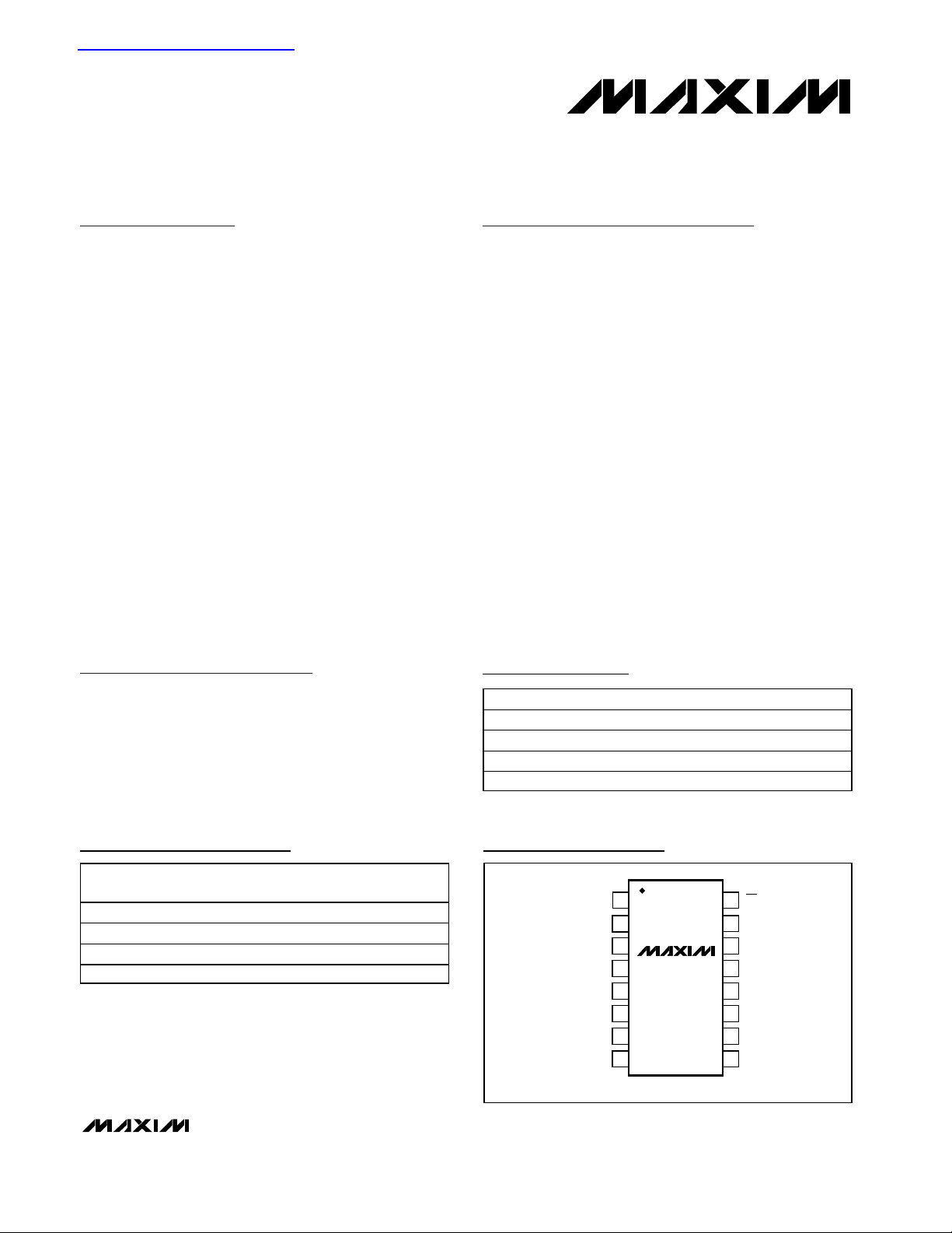
Pin Configuration
Ordering Information
查询MAX1253AEUE供应商
PART INL (LSB)
MAX1253AEUE*
MAX1253BEUE
MAX1254AEUE*
MAX1254BEUE
±1 ±1.0
±1 ±3.0
±1 ±1.0
±1 ±2.5
TEMP
ERROR (°C)
SUPPLY
VOLTAGE (V)
2.7 to 3.6
2.7 to 3.6
4.5 to 5.5
4.5 to 5.5
PART TEMP RANGE PIN-PACKAGE
MAX1253AEUE* -40°C to +85°C
MAX1253BEUE -40°C to +85°C
MAX1254AEUE* -40°C to +85°C
MAX1254BEUE -40°C to +85°C
TOP VIEW
AIN0
AIN1
AIN2
AIN3
AIN4
AIN5
AIN6
AIN7
1
2
3
4
5
6
7
8
MAX1253
MAX1254
16 TSSOP
16
15
14
13
12
11
10
9
16 TSSOP
16 TSSOP
16 TSSOP
16 TSSOP
CS
SCLK
DIN
V
DD
GND
DOUT
INT
REF
Page 2
MAX1253/MAX1254
Stand-Alone, 10-Channel, 12-Bit System Monitors
with Internal Temperature Sensor and V
DD
Monitor
2 _______________________________________________________________________________________
ABSOLUTE MAXIMUM RATINGS
Stresses beyond those listed under “Absolute Maximum Ratings” may cause permanent damage to the device. These are stress ratings only, and functional
operation of the device at these or any other conditions beyond those indicated in the operational sections of the specifications is not implied. Exposure to
absolute maximum rating conditions for extended periods may affect device reliability.
VDDto GND .............................................................-0.3V to +6V
Analog Inputs to GND (AIN0–AIN7, REF) ... -0.3V to (V
DD
+ 0.3V)
Digital Inputs to GND (DIN, SCLK, CS) .... -0.3V to (V
DD
+ 0.3V)
Digital Outputs to GND (DOUT, INT) ........ -0.3V to (V
DD
+ 0.3V)
Digital Outputs Sink Current ............................................. 25mA
Maximum Current into Any Pin .......................................... 50mA
Continuous Power Dissipation (TA= +70°C)
16-Pin TSSOP (derate 8.7mW/°C above +70°C) .........696mW
Operating Temperature Range ...........................-40°C to +85°C
Junction Temperature......................................................+150°C
Storage Temperature Range .............................-65°C to +150°C
Lead Temperature (soldering, 10s) .................................+300°C
ELECTRICAL CHARACTERISTICS
(VDD= +2.7V to +3.6V (MAX1253), VDD= +4.5V to +5.5V (MAX1254), V
REF
= +2.5V (MAX1253), V
REF
= +4.096V (MAX1254), f
SCLK
= 10MHz (50% duty cycle), TA= T
MIN
to T
MAX
, unless otherwise noted. Typical values are at TA= +25°C.)
DC ACCURACY
Resolution RES 12 Bits
Integral Nonlinearity (Note 1) INL
Differential Nonlinearity DNL No missing codes overtemperature ±1.0 LSB
Offset Error ±4.0 LSB
Gain Error (Note 2)
Offset Error Tempco ±5p p m /°C
Gain and Temperature Coefficient
C hannel - to- C hannel Offset M atchi ng ±0.1 LSB
V DD M oni tor Accur acy Internal reference ±2.5 %
DYNAMIC ACCURACY
(10kHz sine-wave input, 2.5V
Signal-to-Noise Plus Distortion SINAD 70 dB
Total Harmonic Distortion THD Up to the 5th harmonic -76 dB
Spurious-Free Dynamic Range SFDR 72 dB
Full-Power Bandwidth -3dB point 1 MHz
Full Linear Bandwidth S / (N + D) > 68dB 100 kHz
CONVERSION RATE
Single-Channel Throughput Manual trigger, voltage measurement 70 ksps
Power-Up Time t
ANALOG INPUT
Input Voltage Range (Note 5)
Common-Mode Range Differentially configured inputs 0 V
Common-Mode Rejection D i ffer enti all y confi g ur ed i np uts, V
PARAMETER SYMBOL CONDITIONS MIN TYP MAX UNITS
P-P
(AIN0–AIN7)
(MAX1253), 4.096V
Grade A ±1.0
Grade B ±1.0
External reference ±4.0 LSB
Internal reference 2.0 %FSR
External reference ±2
Internal reference ±30
Voltage measurement, all ref modes 10.6 11.7
CONV
Temp-sensor ref modes 01, 10 46 50.7Conversion Time (Note 3) t
Temp-sensor ref mode 00 73 80
Internal reference (Note 4) 40 45 µs
PU
U ni p ol ar , si ng l e- end ed , or d i ffer enti al i np uts 0 +V
Bipolar, differential inputs -V
(MAX1254), 64ksps, f
P-P
= 10MHz, bipolar input mode)
SCLK
= 0 to V
C M
D D
/ 2 +V
REF
-90 dB
REF
REF
DD
/ 2
LSB
p p m /°C
µs
V
V
Page 3
MAX1253/MAX1254
Stand-Alone, 10-Channel, 12-Bit System Monitors
with Internal Temperature Sensor and V
DD
Monitor
_______________________________________________________________________________________ 3
ELECTRICAL CHARACTERISTICS (continued)
(VDD= +2.7V to +3.6V (MAX1253), VDD= +4.5V to +5.5V (MAX1254), V
REF
= +2.5V (MAX1253), V
REF
= +4.096V (MAX1254), f
SCLK
= 10MHz (50% duty cycle), TA= T
MIN
to T
MAX
, unless otherwise noted. Typical values are at TA= +25°C.)
Input Leakage Current On-/off-leakage, VIN = 0 or V
Input Capacitance (Note 6) 18 pF
TEMPERATURE MEASUREMENTS
Internal Sensor Measurement Error
(Note 7)
External Sensor Measurement
Error (Note 8)
Temperature Measurement Noise
Temperature Resolution 0.125 °C/LSB
External Sensor Bias Current
Power-Supply Rejection PSR
INTERNAL REFERENCE
REF Output Voltage V
REF Temperature Coefficient TC
REF Output Resistance 7kΩ
REF Output Noise
REF Power-Supply Rejection Ratio PSRR
EXTERNAL REFERENCE
REF Input Voltage Range V
REF Input Current I
PARAMETER SYMBOL CONDITIONS MIN TYP MAX UNITS
Grade A
MAX1253
MAX1254
Grade B
MAX1253
Grade B
MAX1254
Differential
Single ended
Differentially configured inputs and internal
sensor
Single-ended configured, external sensor 0.1
Low 4
High 66
Differentially configured inputs and internal
sensor
Single-ended configured, external sensor 0.1
MAX1253 2.456 2.500 2.544
REF
MAX1254 4.024 4.096 4.168
Grade A ±8
REF
Grade B ±30
MAX1253 200
MAX1254 160
MAX1253 -70 -50
MAX1254 -70 -50
REF
V
= +2.5V; f
REF
REF
In power-down ±1
SAMPLE
DD
TA = -20°C to +85°C ±0.5 ±1.0
TA = -40°C to +85°C ±0.75 ±1.5
= +25°C ±0.3
T
A
TA = -40°C to +85°C ±1.2 ±2.5
T
= +25°C ±0.7
A
TA = -40°C to +85°C ±1.2 ±3.0
= +25°C ±0.7
T
A
TA = -40°C to +85°C±2
= +25°C±1
T
A
TA = -40°C to +85°C±5
T
= +25°C±2
A
= 94ksps 15 40
±1 µA
0.3
0.3
p p m /°C
µV
1.0 VDD + 0.05 V
°C
°C
°C
µA
°C/V
V
RMS
dB
µA
Page 4
MAX1253/MAX1254
Stand-Alone, 10-Channel, 12-Bit System Monitors
with Internal Temperature Sensor and V
DD
Monitor
4 _______________________________________________________________________________________
ELECTRICAL CHARACTERISTICS (continued)
(VDD= +2.7V to +3.6V (MAX1253), VDD= +4.5V to +5.5V (MAX1254), V
REF
= +2.5V (MAX1253), V
REF
= +4.096V (MAX1254), f
SCLK
= 10MHz (50% duty cycle), TA= T
MIN
to T
MAX
, unless otherwise noted. Typical values are at TA= +25°C.)
DIGITAL INPUTS
Input Voltage Low V
Input Voltage High V
Input Hysteresis V
Input Leakage Current I
Input Capacitance C
DIGITAL OUTPUTS
Output Voltage Low V
Output Voltage High V
Tri-State Leakage Current I
Tri-State Output Capacitance C
POWER REQUIREMENTS
Positive Supply Voltage V
Supply Current I
Full Power-Down Supply Current I
Power-Supply Rejection Ratio PSRR Analog inputs at full scale (Note 12) ±0.4 ±1.6 mV/V
PARAMETER SYMBOL CONDITIONS MIN TYP MAX UNITS
(SCLK, DIN, CS)
(INT, DOUT)
IL
IH
HYST
IN
IN
OL
OH
L
OUT
DD
DD
SHDN
VIN = 0 or V
I
SINK
I
SINK
I
SOURCE
I
SOURCE
CS = V
CS = V
MAX1253 2.7 3.6
MAX1254 4.5 5.5
MAX1253 internal reference (Note 9) 3.3
MAX1253 internal reference (Note 10) 2.9
MAX1253 external reference (Note 10) 2.2
MAX1254 internal reference (Note 9) 5.0
MAX1254 internal reference (Note 10) 4.0
MAX1254 external reference (Note 10) 3.0
Both internal reference, mode 01 (Note 11) 8 µA
Full power-down state
DD
= 8mA, DOUT 0.5
= 2mA, INT 0.5
= 8mA, DOUT VDD - 0.5
= 2mA, INT VDD - 0.5
DD
DD
VDD x 0.7 V
MAX1253 480
MAX1254 860
200 mV
VDD x 0.3 V
±10 µA
2pF
±10 µA
5pF
V
V
V
mA
nA
Page 5

MAX1253/MAX1254
Stand-Alone, 10-Channel, 12-Bit System Monitors
with Internal Temperature Sensor and V
DD
Monitor
_______________________________________________________________________________________ 5
Note 1: Relative accuracy is the deviation of the analog value at any code from its theoretical value after the gain and offset errors
have been calibrated.
Note 2: Offset nulled.
Note 3: In reference mode 00, the reference system powers up for each temperature measurement. In reference mode 01, the ref-
erence system powers up once per sequence of channels scanned. If a sample wait <80µs is programmed, the reference
system is on all the time. In reference mode 10, the reference system is on all the time (see Table 7).
Note 4: No external capacitor on REF.
Note 5: The operational input voltage range for each individual input of a differentially configured pair (AIN0–AIN7) is from GND to
V
DD
.
The operational input voltage difference is from -V
REF
/2 to +V
REF
/2.
Note 6: See Figure 3 and the Sampling Error vs. Input Source Impedance graph in the Typical Operating Characteristics section.
Note 7: Grade A tested at +10°C and +55°C. -20°C to +85°C and -40°C to +85°C specifications guaranteed by design. Grade B
tested at +25°C. T
MIN
to T
MAX
specification guaranteed by design.
Note 8: External temperature measurement mode using an MMBT3904 (Diodes Inc.) as a sensor. External temperature sensing
from -40°C to +85°C; MAX1253/MAX1254 held at +25°C.
Note 9: Performing eight single-ended external channels’ temperature measurements, an internal temperature measurement, and
an internal V
DD
measurement with no sample wait results in a conversion rate of 2ksps per channel.
Note 10: Performing eight single-ended voltage measurements, an internal temperature measurement, and an internal V
DD
measure-
ment with no sample wait results in a conversion rate of 7ksps per channel.
Note 11: Performing eight single-ended voltage measurements, an internal temperature measurement, and an internal V
DD
measure-
ment with maximum sample wait results in a conversion rate of 3ksps per channel.
Note 12: Defined as the shift in the code boundary as a result of supply voltage change. V
DD
= min to max; full-scale input, mea-
sured using external reference.
TIMING CHARACTERISTICS
(VDD= +2.7V to +3.6V (MAX1253), VDD= +4.5V to +5.5V (MAX1254), TA= T
MIN
to T
MAX
, unless otherwise noted.) (Figures 1, 2, and 4)
SCLK Clock Period t
SCLK Pulse Width High Time t
SCLK Pulse Width Low Time t
DIN to SCLK Setup Time t
DIN to SCLK Hold Time t
CS Fall to SCLK Rise Setup t
SCLK Rise to CS Rise Hold t
SCLK Fall to DOUT Valid t
CS Rise to DOUT Disable t
CS Fall to DOUT Enable t
CS Pulse Width High t
PARAMETER SYMBOL CONDITIONS MIN TYP MAX UNITS
CP
CH
CL
DS
DH
CSS
CSH
DOV
DOD
DOE
CSW
CL = 30pF 50 ns
CL = 30pF 40 ns
CL = 30pF 40 ns
100 0.5 ns
45 ns
45 ns
25 ns
0ns
25 ns
50 ns
40 ns
Page 6
SUPPLY CURRENT
vs. SAMPLE RATE
MAX1253/54 toc07
SAMPLE RATE (kHz)
SUPPLY CURRENT (mA)
1010.10.01
0.01
0.1
1
10
0.001
0.001 100
INTERNAL REFERENCE
(MODE 01) MAX1254
9 TEMPERATURE
CHANNELS AND 1
VOLTAGE CHANNEL
9 VOLTAGE
CHANNELS AND
1 TEMPERATURE
CHANNEL
1 VOLTAGE CHANNEL
(V
DD
/2)
SUPPLY CURRENT
vs. SUPPLY VOLTAGE
MAX1253/54 toc08
SUPPLY VOLTAGE (V)
SUPPLY CURRENT (mA)
5.14.73.1 3.5 3.9 4.3
1.4
1.8
2.2
2.6
3.0
3.4
3.8
4.2
1.0
2.7 5.5
EXTERNAL REFERENCE (MODE 00)
9 VOLTAGE CHANNELS AND
1 TEMPERATURE CHANNEL
1 VOLTAGE CHANNEL
(V
DD
/2)
9 TEMPERATURE CHANNELS
AND 1 VOLTAGE CHANNEL
REFERENCE VOLTAGE
vs. TEMPERATURE
MAX1253/54 toc05
TEMPERATURE (°C)
REFERENCE VOLTAGE (V)
6040200-20
2.492
2.494
2.496
2.498
2.500
2.502
2.504
2.506
2.508
2.510
2.490
-40 80
GRADE A
GRADE B
MAX1253
REFERENCE VOLTAGE
vs. TEMPERATURE
MAX1253/54 toc05b
TEMPERATURE (°C)
REFERENCE VOLTAGE (V)
6040200-20
4.0725
4.0750
4.0775
4.0800
4.0825
4.0850
4.0875
4.0900
4.0700
-40 80
GRADE A
MAX1254
GRADE B
SUPPLY CURRENT
vs. SAMPLE RATE
MAX1253/54 toc06
SAMPLE RATE (kHz)
SUPPLY CURRENT (mA)
1010.10.01
0.01
0.1
1
10
0.001
0.001 100
INTERNAL REFERENCE
(MODE 01) MAX1253
9 TEMPERATURE
CHANNELS AND 1
VOLTAGE CHANNEL
(V
DD
/2)
9 VOLTAGE
CHANNELS AND
1 TEMPERATURE
CHANNEL
1 VOLTAGE CHANNEL
(V
DD
/2)
INTERNAL REFERENCE VOLTAGE
vs. SUPPLY VOLTAGE
MAX1253/54 toc04
SUPPLY VOLTAGE (V)
INTERNAL REFERENCE VOLTAGE (V)
5.45.35.1 5.24.7 4.8 4.9 5.04.6
4.077
4.079
4.081
4.083
4.085
4.075
4.5 5.5
MAX1254
MAX1253/MAX1254
Stand-Alone, 10-Channel, 12-Bit System Monitors
with Internal Temperature Sensor and V
DD
Monitor
6 _______________________________________________________________________________________
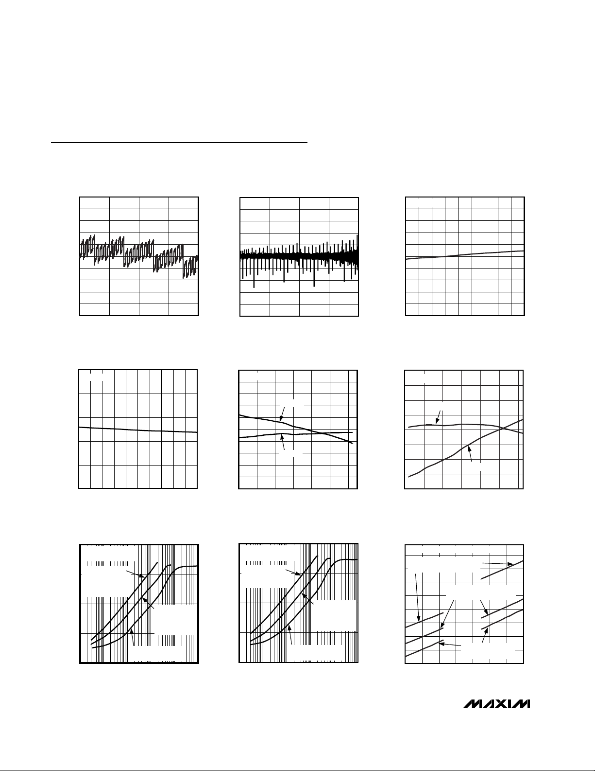
Typical Operating Characteristics
(VDD= +3V, V
REF
= 2.5V (MAX1253); VDD= 5V, V
REF
= 4.096V (MAX1254); f
SCLK
= 10MHz, C
REF
= 0.1µF, TA= +25°C, unless oth-
erwise noted.)
INTEGRAL NONLINEARITY
vs. DIGITAL OUTPUT CODE
MAX1253/54 toc01
OUTPUT CODE
INL (LSB)
307220481024
-0.8
-0.6
-0.4
-0.2
0
0.2
0.4
0.6
0.8
1.0
-1.0
0 4096
DIFFERENTIAL NONLINEARITY
vs. DIGITAL OUTPUT CODE
MAX1253/54 toc02
OUTPUT CODE
DNL (LSB)
307220481024
-0.8
-0.6
-0.4
-0.2
0
0.2
0.4
0.6
0.8
1.0
-1.0
0 4096
INTERNAL REFERENCE VOLTAGE
vs. SUPPLY VOLTAGE
MAX1253/54 toc03
SUPPLY VOLTAGE (V)
INTERNAL REFERENCE VOLTAGE (V)
3.53.43.2 3.32.9 3.0 3.12.8
2.501
2.502
2.503
2.504
2.505
2.506
2.507
2.508
2.509
2.510
2.500
2.7 3.6
MAX1253
Page 7
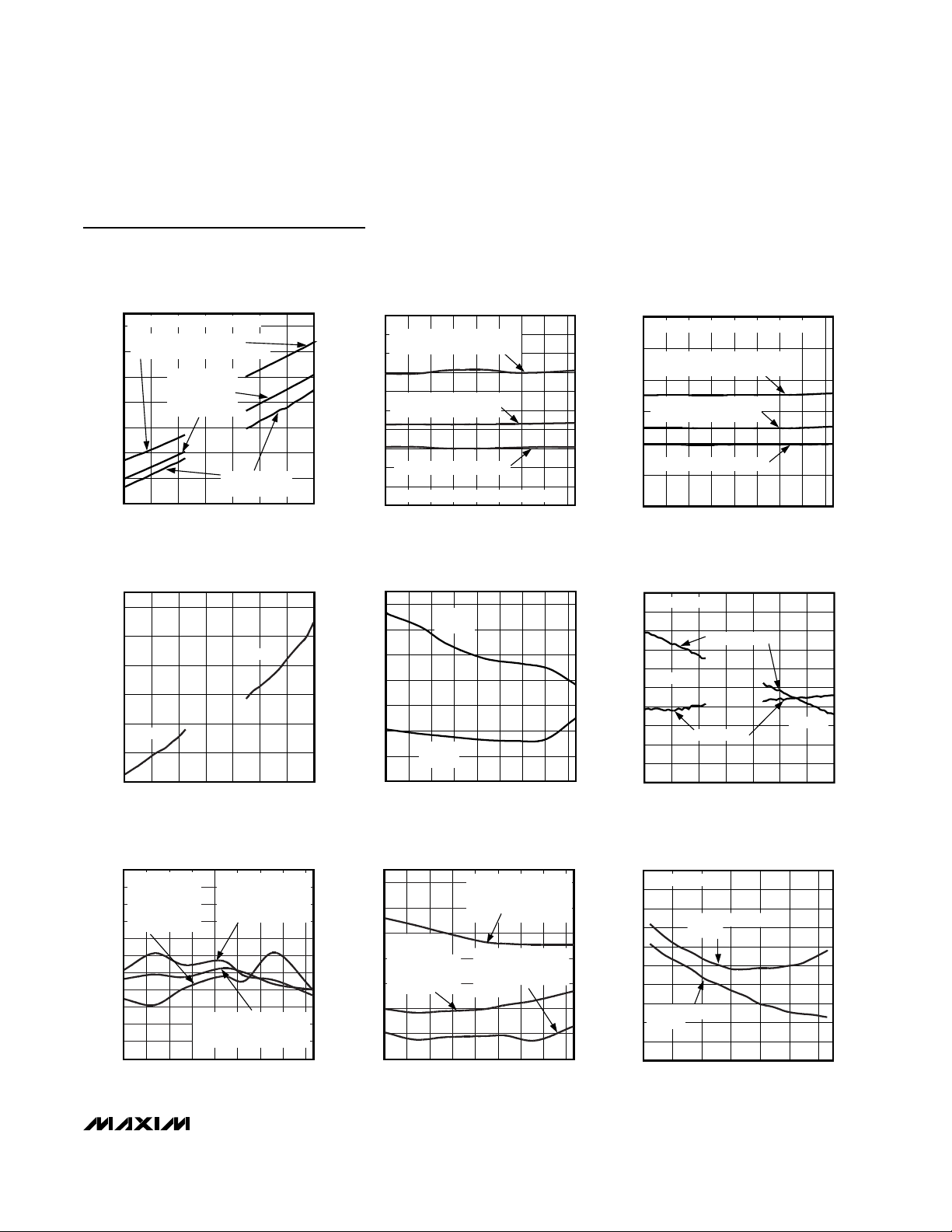
GAIN ERROR vs. TEMPERATURE
MAX1253/54 toc15
TEMPERATURE (°C)
GAIN ERROR (LSB)
80655035205-10-25
0.10
0
0.20
0.40
0.30
0.60
0.50
0.70
0.90
0.80
1.00
-0.10
-40
UNIPOLAR
DIFFERENTIAL
CONFIGURATION
EXTERNAL
REFERENCE MODE
BIPOLAR DIFFERENTIAL
CONFIGURATION
EXTERNAL REFERENCE
MODE
UNIPOLAR SINGLE-ENDED
CONFIGURATION
EXTERNAL REFERENCE MODE
OFFSET ERROR vs. TEMPERATURE
MAX1253/54 toc16
TEMPERATURE (°C)
OFFSET ERROR (LSB)
80655035205-10-25
-0.80
-0.60
-0.40
-0.20
0
0.20
0.40
-1.00
-40
UNIPOLAR
DIFFERENTIAL
CONFIGURATION
EXTERNAL
REFERENCE MODE
BIPOLAR DIFFERENTIAL
CONFIGURATION
EXTERNAL REFERENCE
MODE
UNIPOLAR SINGLE-ENDED
CONFIGURATION
EXTERNAL REFERENCE
MODE
INTERNAL TEMPERATURE SENSOR
TEMPERATURE ERROR
MAX1253/54 toc17
TEMPERATURE (°C)
ERROR (°C)
6040200-20
-0.80
-0.60
-0.40
-0.20
0
0.20
0.40
0.60
0.80
1.00
-1.00
-40 80
MAX1253/MAX1254
GRADE A INTERNAL
SENSOR
GRADE B INTERNAL
SENSOR
MAX1253/MAX1254
Stand-Alone, 10-Channel, 12-Bit System Monitors
with Internal Temperature Sensor and V
DD
Monitor
_______________________________________________________________________________________ 7
Typical Operating Characteristics (continued)
(VDD= +3V, V
REF
= 2.5V (MAX1253); VDD= 5V, V
REF
= 4.096V (MAX1254); f
SCLK
= 10MHz, C
REF
= 0.1µF, TA= +25°C, unless oth-
erwise noted.)
SUPPLY CURRENT
vs. SUPPLY VOLTAGE
MAX1253/54 toc09
SUPPLY VOLTAGE (V)
SUPPLY CURRENT (mA)
5.14.73.1 3.5 3.9 4.3
1.9
2.3
2.7
3.1
3.5
3.9
4.3
1.5
2.7 5.5
INTERNAL REFERENCE (MODE 01)
9 TEMPERATURE CHANNELS
AND VOLTAGE CHANNEL (V
DD
/2)
9 VOLTAGE
CHANNELS AND
1 TEMPERATURE
CHANNEL
1 VOLTAGE
CHANNEL (V
DD
/2)
SUPPLY CURRENT
vs. TEMPERATURE
MAX1253/54 toc10
TEMPERATURE (°C)
SUPPLY CURRENT (mA)
806535 50-10 5 20-25
1.7
1.8
1.9
2.0
2.1
2.2
2.3
2.4
2.5
2.6
1.6
-40
9 TEMPERATURE CHANNELS AND
1 VOLTAGE CHANNEL (V
DD
/2)
9 VOLTAGE CHANNELS AND
1 TEMPERATURE CHANNEL
1 VOLTAGE CHANNEL (VDD/2)
INTERNAL REFERENCE (MODE 01) MAX1253
SUPPLY CURRENT
vs. TEMPERATURE
MAX1253/54 toc11
TEMPERATURE (°C)
SUPPLY CURRENT (mA)
806535 50-10 5 20-25
2.5
3.0
4.0
3.5
4.5
5.0
2.0
-40
9 TEMPERATURE CHANNELS AND
1 VOLTAGE CHANNEL (V
DD
/2)
9 VOLTAGE CHANNELS AND
1 TEMPERATURE CHANNEL
1 VOLTAGE CHANNEL (VDD/2)
INTERNAL REFERENCE (MODE 01) MAX1254
SHUTDOWN SUPPLY CURRENT
vs. SUPPLY VOLTAGE
MAX1253/54 toc12
SUPPLY VOLTAGE (V)
SHUTDOWN SUPPLY CURRENT (nA)
5.14.74.33.93.53.1
200
300
400
500
600
700
100
2.7 5.5
MAX1253
MAX1254
SHUTDOWN SUPPLY CURRENT
vs. TEMPERATURE
MAX1253/54 toc13
TEMPERATURE (°C)
SHUTDOWN SUPPLY CURRENT (nA)
655035205-10-25
100
200
300
400
500
600
700
0
-40 80
MAX1254
V
DD
= 5V
MAX1253
V
DD
= 3V
GAIN AND OFFSET ERROR
vs. SUPPLY VOLTAGE
MAX1253/54 toc14
SUPPLY VOLTAGE (V)
GAIN AND OFFSET ERROR (LSB)
5.14.73.9 4.33.53.1
-0.80
-0.60
-0.40
-0.20
0
0.20
0.40
0.60
0.80
1.00
-1.00
2.7 5.5
SINGLE ENDED
MAX1253
MAX1254
OFFSET ERROR
GAIN ERROR
Page 8
MAX1253/MAX1254
Stand-Alone, 10-Channel, 12-Bit System Monitors
with Internal Temperature Sensor and V
DD
Monitor
8 _______________________________________________________________________________________
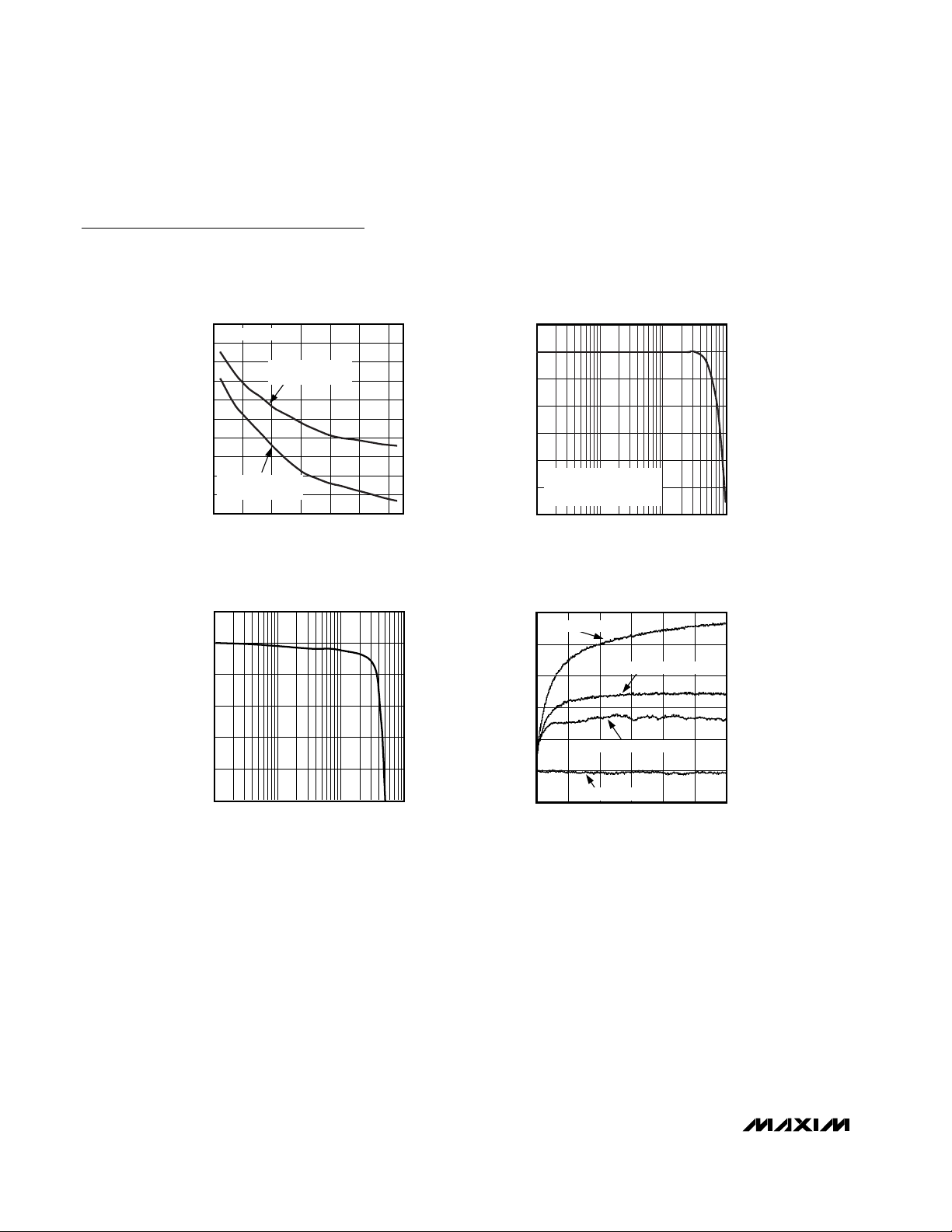
Typical Operating Characteristics (continued)
(VDD= +3V, V
REF
= 2.5V (MAX1253); VDD= 5V, V
REF
= 4.096V (MAX1254); f
SCLK
= 10MHz, C
REF
= 0.1µF, TA= +25°C, unless oth-
erwise noted.)
EXTERNAL TEMPERATURE SENSOR
TEMPERATURE ERROR
2.0
MAX1253/MAX1254
1.6
1.2
0.8
0.4
0
ERROR (°C)
-0.4
-0.8
-1.2
EXTERNAL SENSOR,
SINGLE-ENDED INPUT
-1.6
-2.0
-40 80
EXTERNAL SENSOR,
DIFFERENTIAL INPUT
TEMPERATURE (°C)
SAMPLING ERROR
vs. INPUT SOURCE IMPEDANCE
1
0
-1
MAX1253/54 toc18
6040200-20
MAX1253/54 toc20
TEMPERATURE ERROR vs. INTERCONNECT
CAPACITANCE (EXTERNAL SENSOR)
1
0
-1
-2
-3
TEMPERATURE (°C)
-4
EXTERNAL DIODE
DIFFERENTIAL TEMPERATURE
-5
MEASUREMENT MODE
-6
1
10 100
INTERCONNECT CAPACITANCE (pF)
TURN ON THERMAL TRANSIENT,
CONTINUOUS CONVERSION
V
0.625
IN A TSSOP SOCKET
0.500
0.375
DD
SOLDER ON A 2in ✕ 2in PWB
MAX1253/54 toc19
1000
= 3.0V
MAX1253/54 toc21
-2
-3
SAMPLING ERROR (LSB)
-4
-5
10 10,000
SOURCE IMPEDANCE (Ω)
1000100
0.250
0.125
TEMPERATURE SHIFT (°C)
0
-0.125
030
IN AN OIL BATH
EXTERNAL BJT
252015105
TIME (s)
Page 9
MAX1253/MAX1254
Stand-Alone, 10-Channel, 12-Bit System Monitors
with Internal Temperature Sensor and V
DD
Monitor
_______________________________________________________________________________________ 9
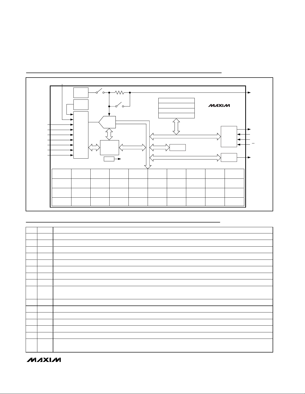
Pin Description
PIN
NAME
FUNCTION
1
Analog Voltage Input/Temperature Input Channel 0 or Positive Differential Input Relative to AIN1
2
Analog Voltage Input/Temperature Input Channel 1 or Negative Differential Input Relative to AIN0
3
Analog Voltage Input/Temperature Input Channel 2 or Positive Differential Input Relative to AIN3
4
Analog Voltage Input/Temperature Input Channel 3 or Negative Differential Input Relative to AIN2
5
Analog Voltage Input/Temperature Input Channel 4 or Positive Differential Input Relative to AIN5
6
Analog Voltage Input/Temperature Input Channel 5 or Negative Differential Input Relative to AIN4
7
Analog Voltage Input/Temperature Input Channel 6 or Positive Differential Input Relative to AIN7
8
Analog Voltage Input/Temperature Input Channel 7 or Negative Differential Input Relative to AIN6
9
Positive Reference Input in External Mode. Bypass REF with a 0.1µF capacitor to GND when in external mode.
When using the internal reference, REF must be left open.
10
Interrupt Output. Push-pull or open drain with selectable polarity. See Table 9 and the INT Interrupt Output section.
11
Serial Data Output. DOUT transitions on the falling edge of SCLK. High impedance when CS is at logic high.
12
Ground
13
Positive Power Supply. Bypass with a 0.1µF capacitor to GND.
14
Serial Data Input. DIN data is latched into the serial interface on the rising edge of the SCLK.
15
Serial Clock Input. Clocks data in and out of the serial interface (duty cycle must be 40% to 60%).
16
Active-Low Chip-Select Input. When CS is low, the serial interface is enabled. When CS is high, DOUT is high
impedance, and the serial interface resets.
Block Diagram
V
DD
REFERENCE
INPUT CHANNEL REGISTER
INPUT CONFIGURATION REGISTER
STEP-UP REGISTER
ALARM REGISTER
AIN3
ACCUMULATOR
THRESHOLD
THRESHOLD
CHANNEL
CONFIGURATION
ACCUMULATOR
UPPER
LOWER
CONFIGURATION
AVERAGING
AIN4
UPPER
THRESHOLD
LOWER
THRESHOLD
CHANNEL
AIN5
ACCUMULATOR
UPPER
THRESHOLD
LOWER
THRESHOLD
CHANNEL
CONFIGURATION
MAX1253
MAX1254
AIN6
ACCUMULATOR
UPPER
THRESHOLD
LOWER
THRESHOLD
CHANNEL
CONFIGURATION
AIN1
AIN2
AIN3
AIN4
AIN5
AIN6
AIN7
INTERNAL TEMP
ACCUMULATOR
UPPER
THRESHOLD
LOWER
THRESHOLD
CHANNEL
CONFIGURATION
TEMP
SENSOR
MUX
/2
V
DD
ACCUMULATOR
UPPER
THRESHOLD
LOWER
THRESHOLD
CHANNEL
CONFIGURATION
ADC WITH
CONVERSION
CONTROL
AIN0
ACCUMULATOR
UPPER
THRESHOLD
LOWER
THRESHOLD
CHANNEL
CONFIGURATION
12-BIT
T/H
SCAN
AND
POR
ACCUMULATOR
THRESHOLD
THRESHOLD
CHANNEL
CONFIGURATION
AIN1
UPPER
LOWER
POWER-
GOOD
AIN2
ACCUMULATOR
UPPER
THRESHOLD
LOWER
THRESHOLD
CHANNEL
CONFIGURATION
REF
DOUT
SERIAL
INTERFACE
DIGITAL
COMPARATOR
AIN7
ACCUMULATOR
UPPER
THRESHOLD
LOWER
THRESHOLD
CHANNEL
CONFIGURATION
DIN
SCLK
CS
INT
AIN0
AIN1
AIN2
AIN3
AIN4
AIN5
AIN6
AIN7
REF
INT
DOUT
GND
V
DD
DIN
SCLK
CS
Page 10

MAX1253/MAX1254
Stand-Alone, 10-Channel, 12-Bit System Monitors
with Internal Temperature Sensor and V
DD
Monitor
10 ______________________________________________________________________________________
Figure 1. Load Circuits for DOUT Enable Time and SCLK to
DOUT Delay Time
Figure 2. Load Circuit for DOUT Disable Time
Detailed Description
The MAX1253/MAX1254 are precision-monitoring integrated circuit systems specifically intended for standalone operation. They can monitor diverse types of
inputs, such as those from temperature sensors and
voltage signals from pressure, vibration, and acceleration sensors, and digitize these input signals. The digital values are then compared to preprogrammed
thresholds and, if the thresholds are exceeded, the
processor is alerted by an interrupt signal. No interaction by the CPU or microcontroller (µC) is required until
one of the programmed limits is exceeded (Figures 3
and 4).
Voltages on all the inputs are converted to 12-bit values
sequentially and stored in the current data registers.
Note that eight of these inputs are external and two are
internal. One of the internal inputs monitors the V
DD
voltage supply, while the other monitors the internal IC
temperature. AIN0 to AIN7 can be configured as either
single ended (default) or differential. In addition, these
inputs can be configured for single-ended or differential temperature measurements. In the temperature
configuration, the device provides the proper bias necessary to measure temperature with a diode-connected
transistor sensor. The user enables which inputs are
measured (both external and internal) and sets the
delay between each sequence of measurements during the initial setup of the device.
The values stored in the current data registers are compared to the user-preprogrammed values in the threshold registers (upper and lower thresholds) and, if
exceeded, activate the interrupt output and generate an
alarm condition. If desired, the device can be programmed to average the results of many measurements
before comparing to the threshold value. This reduces
the sensitivity to external noise in the measured signal.
In addition, the user can set the number of times the
threshold is exceeded (fault cycles) before generating
an interrupt. This feature reduces falsely triggered
alarms caused by undesired, random spurious impulses.
When the fault cycle criterion is exceeded, an alarm
condition is created. The device writes the fault condition into the alarm register to indicate the alarmed input
channel.
Converter Operation
The MAX1253/MAX1254 ADCs use a fully differential
successive-approximation register (SAR) conversion
technique and an on-chip track-and-hold (T/H) block to
convert temperature and voltage signals into a 12-bit
digital result. Both single-ended and differential configurations are supported with a unipolar signal range for
single-ended mode and bipolar or unipolar ranges for
differential mode. Figure 5 shows the equivalent input
circuit for the MAX1253/MAX1254. Configure the input
channels according to Tables 5 and 6 (see the Input
Configuration Register section).
In single-ended mode, the positive input (IN+) is connected to the selected input channel and the negative
input (IN-) is connected to GND. In differential mode,
IN+ and IN- are selected from the following pairs:
AIN0/AIN1, AIN2/AIN3, AIN4/AIN5, and AIN6/AIN7.
Once initiated, voltage conversions require 10.6µs (typ)
to complete.
V
DD
100nA
DOUT
100nA
a) V
OL
GND
TO V
C
= 100pF
LOAD
OH
DOUT
C
= 100pF
LOAD
GND
b) HIGH-Z TO VOL AND VOH TO V
OL
DOUT
100nA
GND
TO HIGH-Z
a) V
OH
C
V
100nA
DOUT
GND
b) VOL TO HIGH-Z
LOAD
= 100pF
DD
C
= 100pF
LOAD
Page 11

MAX1253/MAX1254
Stand-Alone, 10-Channel, 12-Bit System Monitors
with Internal Temperature Sensor and V
DD
Monitor
______________________________________________________________________________________ 11
During the acquisition interval, IN+ and IN- charge both
a positive (CHOLDP) and a negative (CHOLDN) sampling capacitor. After completing the acquisition interval, the T/H switches open, storing an accurate sample
of the differential voltage between IN+ and IN-. This
charge is then transferred to the ADC and converted.
Finally, the conversion result is transferred to the current data register.
Temperature conversions require 46µs (typ) and measure the difference between two sequential voltage
measurements (see the Temperature Measurement
section for a detailed description).
Fully Differential Track/Hold (T/H)
The T/H acquisition interval begins with the rising edge
of CS (for manually triggered conversions) and is internally timed to 1.5µs (typ). The accuracy of the input signal sample is a function of the input signal’s source
impedance and the T/H’s capacitance. In order to
achieve adequate settling of the T/H, limit the signal
source impedance to a maximum of 1kΩ.
Input Bandwidth
The ADC’s input tracking circuitry has a 1MHz smallsignal bandwidth. To avoid high-frequency signals
aliasing into the frequency band of interest, anti-alias
prefiltering of the input signals is recommended.
Analog Input Protection
Internal protection diodes, which clamp the analog
inputs to VDDand GND, allow the channel input pins to
swing from (GND - 0.3V) to (VDD+ 0.3V) without damage. However, for accurate conversions near full scale,
the inputs must not exceed VDDby more than 50mV or
be lower than GND by 50mV. If the analog input range
must exceed 50mV beyond the supplies, limit the input
current.
Single Ended/Differential
The MAX1253/MAX1254 use a fully differential ADC for
all conversions. Through the input configuration register, the analog inputs can be configured for either differential or single-ended conversions. When sampling
signal sources close to the MAX1253/MAX1254, singleended conversion is generally sufficient. Single-ended
conversions use only one analog input per signal
source, internally referenced to GND.
Figure 3. Simplified Alarm Block Diagram of the MAX1253/MAX1254
V
DD
AIN0
AIN1
AIN2
AIN3
AIN4
AIN5
AIN6
AIN7
MUX
TEMP
SENSE
12-BIT
ADC WITH T/H
INPUT REGISTERS
CURRENT DATA
UPPER THRESHOLD
LOWER THRESHOLD
# FAULT CYCLES
AVERAGE
CONFIGURATION/
STATUS
REGISTERS
SCAN AND
CONVERSION
CONTROL
DIGITAL
COMPARATOR
SERIAL
INTERFACE
INT
DIN
DOUT
SCLK
CS
Page 12
MAX1253/MAX1254
Stand-Alone, 10-Channel, 12-Bit System Monitors
with Internal Temperature Sensor and V
DD
Monitor
12 ______________________________________________________________________________________
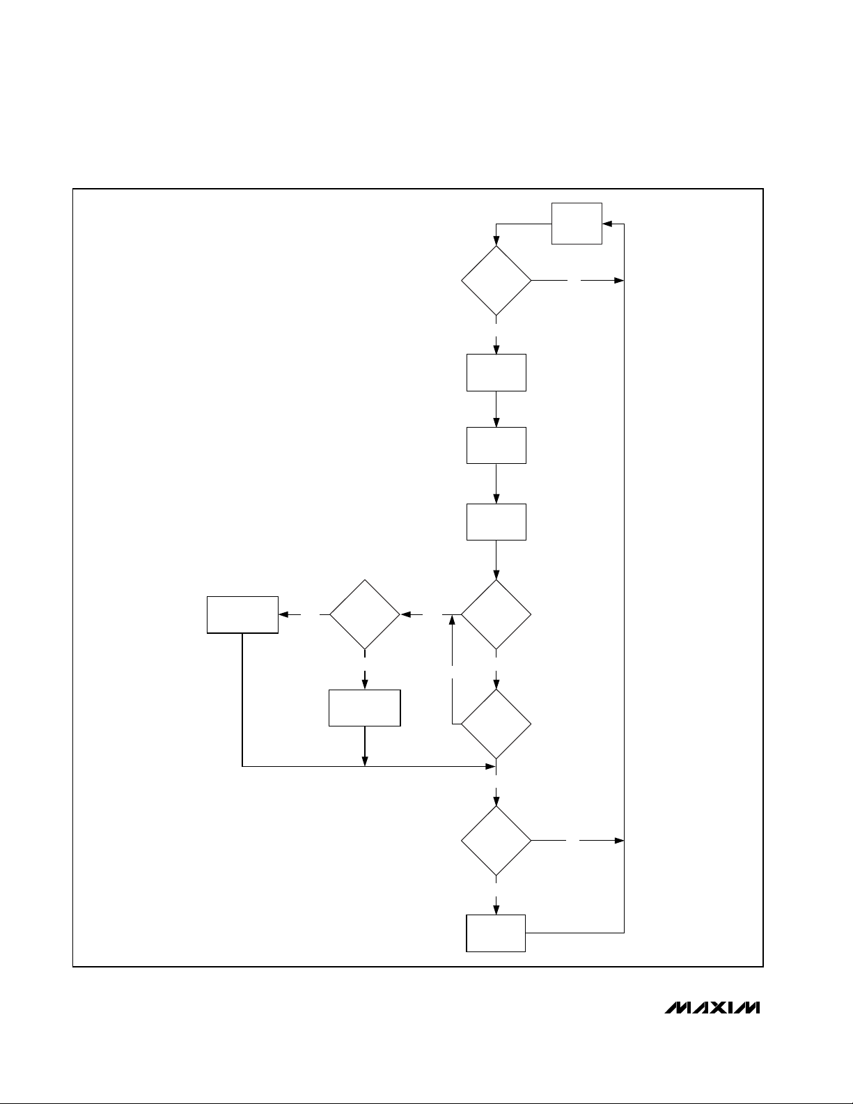
Figure 4. Alarm Flowchart
IS CHANNEL
ENABLED?
YES
SAMPLE
CHANNEL
CONVERT
CHANNEL
AVERAGE
CONVERTED
CHANNEL DATA
INCREMENT
CHANNEL
COUNTER
NO
INCREMENT
FAULT COUNTER
YES
SAME FAULT
AS PREVIOUS?
NO
RESET FAULT
COUNTER
YES
YES
IS
AVG DATA
> UPPER?
NO
IS
AVG DATA
< LOWER?
NO
IS
FAULT CNT
>
FAULT REG?
YES
SET ALARM
REGISTER
NO
Page 13

MAX1253/MAX1254
Stand-Alone, 10-Channel, 12-Bit System Monitors
with Internal Temperature Sensor and V
DD
Monitor
______________________________________________________________________________________ 13
In differential mode, the T/H samples the difference
between two analog inputs, eliminating common-mode
DC offsets and noise. See the Input Configuration
Register section and Tables 5 and 6 for more details on
configuring the analog inputs.
Unipolar/Bipolar
When performing differential conversions, the input
configuration register (Tables 5 and 6) also selects
between unipolar and bipolar operation. Unipolar mode
sets the differential input range from 0 to V
REF.
A negative differential analog input in unipolar mode causes
the digital output code to be zero. Selecting bipolar
mode sets the differential input range to ±V
REF
/2. The
digital output code is straight binary in unipolar mode
and two’s complement in bipolar mode (see the
Transfer Function section).
In single-ended mode, the MAX1253/MAX1254 always
operate in unipolar mode. The analog inputs are internally referenced to GND with a full-scale input range
from 0 to V
REF.
Digital Interface
The MAX1253/MAX1254 digital interface consists of
five signals: CS, SCLK, DIN, DOUT, and INT. CS,
SCLK, DIN, and DOUT comprise an SPI™-compatible
serial interface (see the Serial Digital Interface section).
INT is an independent output that provides an indication that an alarm has occurred in the system (see the
INT Interrupt Output section).
Serial Digital Interface
The MAX1253/MAX1254 feature a serial interface compatible with SPI, QSPI™, and MICROWIRE™ devices.
For SPI/QSPI, ensure that the CPU serial interface runs
in master mode so it generates the serial clock signal.
Select a serial clock frequency of 10MHz or less, and
set clock polarity (CPOL) and phase (CPHA) in the µP
control registers to the same value, one or zero. The
MAX1253/MAX1254 support operation with SCLK idling
high or low, and thus operate with CPOL = CPHA = 0 or
CPOL = CPHA = 1.
Figure 5. Single-Ended/Differential Input Equivalent Input Circuit
SPI and QSPI are trademarks of Motorola, Inc.
MICROWIRE is a trademark of National Semiconductor Corp.
V
DD
T
CHOLDP CHOLD
8-TO-1
DIFFERENTIAL
MUX
TEMP
DIFFERENTIAL INPUT EQUIVALENT INPUT CIRCUIT
H
CHOLDN
T
TT
HH
V
AZ
ADC
V
DD
T
8-TO-1
DIFFERENTIAL
MUX
TEMP
SINGLE-ENDED INPUT EQUIVALENT INPUT CIRCUIT
H
T
H
V
AZ
ADC
Page 14

MAX1253/MAX1254
Stand-Alone, 10-Channel, 12-Bit System Monitors
with Internal Temperature Sensor and V
DD
Monitor
14 ______________________________________________________________________________________
Clock pulses on SCLK shift data into DIN on the rising
edge of the SCLK and out of DOUT on the falling edge
of SCLK.
Data transfers require a logic low on CS. A high-to-low
transition of CS marks the beginning of a data transfer. A
logic high on CS at any time resets the serial interface.
See Figure 6 and the Timing Characteristics table for
detailed serial-interface timing information.
Input Data Format
Serial communications always begin with an 8-bit command word, serially loaded from DIN. A high-to-low
transition on CS initiates the data input operation. The
command word and the subsequent data bytes (for
write operations) are clocked from DIN into the
MAX1253/MAX1254 on the rising edges of SCLK. The
first rising edge on SCLK, after CS goes low, clocks in
the MSB of the command word (see the Command
Word section). The next seven rising edges on SCLK
complete the loading of the command word into the
internal command register. After the 8-bit command
word is entered, transfer 0 to 20 bytes of data, depending on the command. Table 2 shows the number of
data bytes for each command.
Output Data Format
Output data from the MAX1253/MAX1254 is clocked
onto DOUT on the falling edge of SCLK. Single-ended
and unipolar differential measurements are output in
straight binary MSB first, with two 8-bytes-per-conversion result, and the last 4 bits padded with zeros. For
temperature and bipolar differential voltage measurements, the output is two’s complement binary in the
same 2-byte format. The MSB of the output data from a
read command transitions at DOUT after the falling
edge of the 8th SCLK clock pulse following the CS
high-to-low transition. Table 2 shows the number of
bytes to be read from DOUT for a given read command.
Command Word
The command word (Table 1) controls all serial communications and configuration of the MAX1253/
MAX1254, providing access to the 44 on-chip registers.
The first 4 MSBs of the command word specify the
command (Table 2), while the last 4 bits provide
address information.
The first rising edge on SCLK, after CS goes low, transfers the command word MSB into DIN. The next seven
rising edges on SCLK shift the remaining 7 bits into the
internal command register (see the Serial Digital
Interface section).
Figure 6. Detailed Serial Interface Timing Diagram
Table 1. Command Word
B7 (MSB) B6 B5 B4 B3 B2 B1 B0 (LSB)
Command B3
Address B0
CS
SCLK
DIN
DOUT
HIGH-Z
t
CSS
t
DS
t
DH
t
DOE
t
t
CH
CL
t
CP
t
DOV
t
CSH
t
CSW
t
DOD
HIGH-Z
Command B2 Command B1 Command B0 Address B3 Address B2 Address B1
Page 15

MAX1253/MAX1254
Stand-Alone, 10-Channel, 12-Bit System Monitors
with Internal Temperature Sensor and V
DD
Monitor
______________________________________________________________________________________ 15
Manually Triggered Conversion
(Command Code = 0000)
Before beginning a manual conversion, ensure the
scan mode bit in the setup register is zero, because a
logic 1 disables manual conversions. The address bits
in a Manually Triggered Conversion command select
the input channel for conversion (see Table 3). When
performing a differential conversion, use the even channel address (AIN0, AIN2, AIN4, AIN6); the command is
ignored if odd channel addresses (AIN1, AIN3, AIN5,
AIN7) are used for a differential conversion.
After issuing a Manually Triggered Conversion command, bring CS high to begin the conversion. To obtain
a correct conversion result, CS must remain high for a
period longer than the reference power-up time (if in
power-down mode) plus the conversion time for the
selected channel configured conversion type (voltage
or temperature). The conversion’s result can then be
read at DOUT by issuing a Read Current Data Register
for Selected Channel command, addressing the converted channel. See Table 3 for channel addresses.
Table 2. Command Description
DATA BYTES AFTER
COMMAND WORD
COMMAND
WORD
DIN
BYTES
COMMAND DESCRIPTION
0000#### 0 0 Manually Trigged Conversion
0001xxxx 0 3 Read Alarm Register
0010#### 0 2 Read Current Data Register for Selected Channel
0011#### 0 20 Read Current Data Register for All Channels
0100#### 0 5 Read Configuration Register for Selected Channel
0101xxxx 0 5 Read Global Configuration Registers
0110xxxx N/A N/A Reserved
0111xxxx 0 0 Reset
1000#### 0 0 Clear Alarm/Fault for Selected Channels
1001xxxx 0 0 Clear Alarm/Fault for All Channels
1010#### 2 0 Write Current Data Register for Selected Channel
1011xxxx 20 0 Write Current Data Registers for All Channels
1100#### 5 0 Write Configuration Registers for Selected Channel
1101xxxx 5 0 Write Global Configuration Registers
1110xxxx N/A N/A Reserved
1111xxxx N/A N/A Reserved
#### = Channel address code, see Table 3.
xxxx = These bits are ignored for this command.
Table 3. Channel Address
BYTES TO
FROM DOUT
ADDRESS IN COMMAND INPUT
0000 Internal temperature
0001 VDD
0010 AIN0
0011 AIN1
0100 AIN2
0101 AIN3
0110 AIN4
0111 AIN5
1000 AIN6
1001 AIN7
1010 Reserved
1011 Reserved
1100 Reserved
1101 Reserved
1110 Reserved
1111 Reserved
Page 16

MAX1253/MAX1254
Stand-Alone, 10-Channel, 12-Bit System Monitors
with Internal Temperature Sensor and V
DD
Monitor
16 ______________________________________________________________________________________
Read Alarm Register
(Command Code 0001)
The Read Alarm Register command, 0001, outputs the
current status of the alarm register (see Table 11). The
address bits in this command are ignored. The alarm
register is 24 bits long and outputs in 3 bytes. Table 12
illustrates the encoding of the alarm register.
After receiving an interrupt, read the alarm register to
determine the source of the interrupt (see the Alarm
Register section).
Read Current Data Register for Selected
Channel (Command Code 0010)
The Read Current Data Register for Selected Channel
command, 0010, outputs the data in the current data
register of the selected channel. The address bits following this command select the input channel to be
read (see Table 3). The current data register is a 12-bit
register. It takes 2 bytes to read its value. See the
Output Data Format and Current Data Registers sections for more details. See Table 3 for channel addresses. Also, see Figure 7.
Read Current Data Register for All
Channels (Command Code 0011)
The Read Current Data Registers for All Channels command, 0011, outputs the data in the current data registers of all 10 channels starting with the internal
temperature sensor, then the VDDmonitor, followed by
AIN0 to AIN7. The address bits following this command
are ignored. It takes 20 bytes to read all of the 10 channels’ current data registers.
Read Configuration Register for Selected
Channel (Command Code 0100)
The Read Configuration Register for Selected Channel
command, 0100, outputs the configuration data of the
channel selected by the address bits (see Table 3).
The first register that shifts out is the upper threshold
register (2 bytes), followed by the lower threshold register (2 bytes), ending with the channel configuration register (1 byte), all MSB first. It takes 5 bytes to read all
three registers. See the Channel Registers section for
more details.
Figure 7. Serial Register Read Timing
CS
SCLK
DIN
DOUT
C3 C2 C1 C0 A2 A1 A0
A3
D11 D10 D9 D8 D7 D6 D5 D4 D3 D2 D1 D0
Page 17

MAX1253/MAX1254
Stand-Alone, 10-Channel, 12-Bit System Monitors
with Internal Temperature Sensor and V
DD
Monitor
______________________________________________________________________________________ 17
Read Global Configuration Register
(Command Code 0101)
The Read Global Configuration Register command,
0101, outputs the global configuration registers. The
address bits following this command are ignored.
When the MAX1253/MAX1254 receive a read global
configuration register command, they output 5 bytes of
data: 2 bytes from the channel enable register, 2 bytes
from the input configuration register, and 1 byte from
the setup register, all MSB first. See the Global
Configuration Registers section for more details.
RESET (Command Code 0111)
The RESET command, 0111, resets the device. This
command returns the MAX1253/MAX1254 to their
power-on reset state, placing the device into shutdown
mode. The address bits in the command are ignored.
See the Power-Up/Reset Defaults Summary section for
more details.
Clear Channel Alarm for Selected Channel
(Command Code 1000)
The Clear Channel Alarm command, 1000, clears the
alarm bits in the alarm register and resets the fault
counter for the addressed channel. See the Alarm
Register section for more details. See Table 3 for channel addresses.
Clear Alarm Register for All Channels
(Command Code 1001)
The Clear Alarm Register for All Channels command,
1001, clears the entire alarm register and resets the
fault counters for the internal TEMP sensor, the V
DD
monitor, and the AIN0–AIN7 channels. The address bits
in the command are ignored. See the Alarm Register
section for more details.
Write Current Data Register for Selected
Channel (Command Code 1010)
The Write Current Data Register for Selected Channel
command, 1010, writes to the addressed channel’s current data register. This command sets an initial condition when using the averaging filter option (see the
Averaging section). This command can also be used for
testing the thresholds, fault counters, and alarm functions (Figure 8). See Table 3 for channel addresses.
Write Current Data Register for All
Channels (Command Code 1011)
The Write Current Data Register for All Channels command, 1011, writes to the current data registers of all
channels sequentially, starting with the internal temperature sensor, then the VDDmonitor, followed by channels AIN0 to AIN7. The address bits are ignored. Use
this command for testing and setting initial conditions
when using the averaging filter option (see the
Averaging section).
Figure 8. Serial Register Write Timing
CS
SCLK
DIN
DOUT
C3 C2 C1 C0 A2 A1 A0 D11 D10 D9 D8 D7 D6 D5 D4 D3 D2 D1 D0
HIGH-Z
A3
HIGH-Z
Page 18

MAX1253/MAX1254
Stand-Alone, 10-Channel, 12-Bit System Monitors
with Internal Temperature Sensor and V
DD
Monitor
18 ______________________________________________________________________________________
Write-Selected Channel Configuration
Registers (Command Code 1100)
The Write-Selected Channel Configuration Register command, 1100, writes to the three channel configuration
registers for the addressed channel (see Table 3). The
first register to be written is the upper threshold (2 bytes),
followed by the lower threshold (2 bytes), ending with the
channel configuration register (1 byte), all MSB first.
Writing to the configuration registers resets the alarm register bits and the fault counters for the addressed channel. See the Channel Registers section for more details.
Write Global Configuration Registers
(Command Code 1101)
The Write Global Configuration Registers command,
1101, writes to three registers: the channel-enable register (2 bytes), the input configuration register (2 bytes),
and the setup register (1 byte). The command address
bits are ignored. See the Global Configuration
Registers section for more details.
Global Configuration Registers
The global configuration registers consist of the channel-enable register, the input configuration register, and
the setup register. These registers hold configuration
data common to all channels.
Channel-Enable Register
The channel-enable register (Table 4) controls which
channels are converted while in automatic scan mode.
The register contents are ignored for manual conversion commands. Each input channel has a corresponding bit in the channel-enable register. A logic high
enables the corresponding analog input channel for
conversion, while a logic low disables it. In differential
configuration, the bits for odd channels are ignored. At
power-up and after a RESET command, the register
contents default to 111111111111b (all channels
enabled).
Input Configuration Register
The input configuration register (Table 5) stores the
configuration code for each channel as a 3-bit per
channel-pair code (see Table 6), selecting from five
input signal configurations: single-ended unipolar voltage, single-ended temperature, differential unipolar
voltage, differential bipolar voltage, and differential
temperature. Table 5 shows the input configuration register format, and Table 6 shows the 3-bit encoding for
channel configuration. At power-up and after a RESET
command, the register contents defaults to
000000000000b (all inputs single ended).
Table 4. Channel-Enable Register Format
B11
(MSB)
B10 B9 B8 B7 B6 B5 B4 B3 B2 B1
B0
(LSB)
TEMP
VDD AIN0 AIN1 AIN2 AIN3 AIN4 AIN5 AIN6 AIN7 Res Res
Table 5. Input Configuration Register Format
B11
(MSB)
B10 B9 B8 B7 B6 B5 B4 B3 B2 B1
B0
(LSB)
AIN0 and AIN1 configuration
AIN6 and AIN7 configuration
Table 6. Channel Configuration Coding (3 Bits/Channel Pair)
CODE
AIN0, AIN2, AIN4, AIN6 CONFIGURATION AIN1, AIN3, AIN5, AIN7 CONFIGURATION
000 Single-ended input (power-up state) Single-ended input (power-up state)
001 Single-ended input Single-ended, external temperature sensor input
010 Single-ended, external temperature sensor input Single-ended input
011 Single-ended, external temperature sensor input Single-ended, external temperature sensor input
100 Differential unipolar encoded, positive input Differential unipolar encoded, negative input
101 Differential bipolar encoded, positive input Differential bipolar encoded, negative input
110
Differential external temperature sensor, negative input
111 Reserved Reserved
AIN2 and AIN3 configuration AIN4 and AIN5 configuration
Differential external temperature sensor, positive input
Page 19

MAX1253/MAX1254
Stand-Alone, 10-Channel, 12-Bit System Monitors
with Internal Temperature Sensor and V
DD
Monitor
______________________________________________________________________________________ 19
Setup Register
The 8-bit setup register (Table 7) holds configuration
data common to all input channels. At power-up and
after a RESET command, this register defaults to
00000000b.
Setup Register: Sample Wait Bits (B7, B6, B5)
These 3 bits in the setup register (Table 8) set the wait
time between conversion scans. The following are
examples of how the MAX1253/MAX1254 begin a sample sequence (see the Setup Register: Reference
Selection Bits (B1, B0) section).
Operating in reference mode 00 (external reference for
voltage conversions, internal reference for temperature
conversions):
1) Convert the first-enabled channel. If this channel is a
temperature measurement, power up the internal reference (this takes 20µs for each enabled temperature measurement in reference mode 00).
2) Sequence to the next-enabled channel until all channels have been converted.
3) Wait the sample wait period.
4) Repeat the procedure.
Operating in reference mode 01 (internal reference for all
conversions, can be powered down between scans):
1) Power up the internal reference, if powered down
(this takes 40µs).
2) Convert the first-enabled channel, starting with the
internal temperature sensor, if enabled.
3) Sequence to the next-enabled channel until all
enabled channels have been converted.
4) Wait the sample wait time, and enter internal reference power-down mode if this period is greater than
80µs.
5) Repeat the above steps.
Operating in reference mode 10 (internal reference for
all conversions, continuously powered up):
1) Convert the first-enabled channel.
2) Sequence to the next-enabled channel until all
enabled channels have been converted.
3) Wait the sample wait time.
4) Repeat the procedure.
Use the sample wait feature to reduce supply current
when measuring slow-changing analog signals. This
power savings occurs when reference mode 00 or 01 is
used in combination with wait times longer than 80µs.
With reference mode 10 or wait times of less than 80µs,
the internal reference system remains powered up, minimizing any power savings. See the Computing Data
Throughput section. Table 8 shows the B7, B6, B5 wait
time encoding.
Setup Register: Interrupt Control (B4, B3)
Bits B3 and B4 in the setup register configure INT and
how it responds to an alarm event (see the Alarm
Register section). Table 9 shows the available INT
options.
Table 7. Setup Register Format
B7 (MSB) B6 B5 B4 B3 B2 B1 B0 (LSB)
Sample wait bits
Interrupt
active
Interrupt
polarity
Scan
mode
Reference
source B1
Reference
source B2
Table 8. Wait Time Encoding
Table 9. Interrupt Control
B7, B6, B5 WAIT TIME (ms)
000 0
001 0.080
010 0.395
011 1.310
100 4.970
101 19.600
110 78.200
111 312.000
BIT FUNCTION
Output
B4
driver type
Output
B3
polarity
BIT
STATE
1 Driven high or low at all times
High-Z when inactive, driven (high
0
or low) when active
1Acti ve = hig h, i nacti ve = low or hig h- Z
0Acti ve = l ow , inacti ve = hig h or hig h- Z
INT OPERATION
Page 20

MAX1253/MAX1254
Stand-Alone, 10-Channel, 12-Bit System Monitors
with Internal Temperature Sensor and V
DD
Monitor
20 ______________________________________________________________________________________
Setup Register: Scan Mode Bit (B2)
The scan mode bit selects between automatic scanning and manual conversion mode.
When set (B2 = 1), the MAX1253/MAX1254 enter automatic scanning mode and convert every enabled channel starting with the internal temperature sensor,
followed by the V
DD
monitor, then sequencing through
AIN0 to AIN7.
After converting all the enabled channels, the
MAX1253/MAX1254 enter a wait state set by the sample wait bits in the setup register. After completing the
sample wait time, the scan cycle repeats.
When B2 = 0, the MAX1253/MAX1254 are in manual
mode and convert only the selected channel after
receiving a Manually Triggered Conversion command
(see the Manually Triggered Conversion (Command
Code 0000) section). Whether in automatic scanning
mode or manual mode, a Read Current Data Register
for Selected Channel command outputs the last-completed conversion result for the addressed channel at
DOUT.
Setup Register: Reference Selection Bits (B1, B0)
The MAX1253/MAX1254 can be used with an internal
or external reference. Select between internal and
external reference modes through bits B1 and B0 of the
setup register (see Table 10).
Alarm Register
The alarm register (Table 11) holds the current alarm status for all of the monitored signals. This 24-bit register
can only be read and cleared. The alarm register has 2
bits for each external input channel, 2 for the onboard
temperature sensor, and 2 for the V
DD
monitor (see
Table 12). At power-up, these bits are logic low, indicating no alarms at any input. When any bit in the alarm register is set, INT becomes active and remains active until
all alarm bits are cleared. After a fault counter exceeds
the set threshold, the alarm register bits for that particular
channel are updated to indicate an alarm.
To clear the interrupt, reset the active alarm bit with the
Clear Alarm Register command, Clear Channel Alarm
command, a RESET command, or by writing a new
configuration to the faulting channel. The alarm register
defaults to 000000 hex.
Table 11 illustrates how the alarm register stores the
information on which channel a fault has occurred. The
alarm code for each bit pair is shown in Table 12.
Channel Registers
Each channel (internal temperature sensor, VDDmonitor, and AIN0 to AIN7) has registers to hold the conversion result (current data register) and channel-specific
configuration data. The channel-specific configuration
registers include: the upper threshold register, the
lower threshold register, and the channel configuration
register. In differential mode, only the registers for the
even channel of the differential input pair are used. The
channel-specific configuration registers for the odd
channel of a differential channel pair are ignored.
Table 10. Reference Selection
Table 11. Alarm Register Format
B23/B22
B1/B0
TEMP
V
DD
AIN0 AIN1 AIN2 AIN3 AIN4 AIN5 AIN6 AIN7 Res Res
Table 12. Alarm Register Coding
(2 Bits/Channel)
B1 B0 REFERENCE MODE
Voltage measurements use external reference,
while temperature measurements use the internal
00
01
10
1 1 Reserved.
reference. A 20µs reference startup delay is
added prior to each temperature measurement
in this mode. This is the default mode after
power-up and after a software RESET.
All measurements use the internal reference. A
40µs reference startup delay is added prior to
starting the scanning of enabled channels,
allowing the internal reference to stabilize.
Note:
reference is continuously powered when in
automatic scan mode.
All measurements use the internal reference. By
selecting this mode, the reference is powered up
immediately when CS goes high after writing this
configuration. Once the reference system is
powered up, no further delay is added.
For sample wait times less than 80µs, the
CODE DESCRIPTION
00 No alarm (power-up state)
01 Input is below lower threshold
10 Input is above upper threshold
00 Reserved
B21/B20 B19/B18 B17/B16 B15/B14 B13/B12 B11/B10 B9/B8 B7/B6 B5/B4 B3/B2
Page 21

MAX1253/MAX1254
Stand-Alone, 10-Channel, 12-Bit System Monitors
with Internal Temperature Sensor and V
DD
Monitor
______________________________________________________________________________________ 21
Channel Configuration Register
Each channel has a channel configuration register
(Table 13) defining the number of consecutive faults to
be detected before setting the alarm bits and generating an interrupt, as well as controlling the digital averaging. At power-up and after a RESET command, the
register defaults to 00 hex (no averaging, alarm on first
fault).
Fault Bits
The value stored in the fault bits (B7–B4) in the channel
configuration register sets the number of faults that
must occur for that channel before generating an interrupt. Encoding of the fault bits is straight binary with
valves 0 to 15. A fault occurs in a channel when the
value in its current data register is outside the range
defined by the channel’s upper and lower threshold
registers. For example, if the number of faults set by the
fault bits is N, an interrupt is generated when the number of consecutive faults (see note below) reach (N +
1). The fault bits default to 0 hex at power-up.
Note: Consecutive faults are those happening in consecutive conversion scans for the same channel. If a
fault occurs and the next scan finds the input within the
normal range defined by the thresholds, the fault
counter resets. If the next counter finds the input signal
outside the opposite threshold, rather than the previous
one, the fault counter also resets. The fault counter
increments only when counting consecutive faults
exceeding the same threshold (Figure 4).
Averaging
The averaging calculated by the data-acquisition algorithm of the MAX1253/MAX1254 improves the input signal-to-noise ratio (SNR) by reducing the signal
bandwidth digitally. The formula below describes the
filter implemented in the MAX1253/MAX1254:
current value = [(N - 1) / N] x past value +
[(present value) / N]
where N = number of samples indicated in Table 14.
The averaging bits (B3–B0) in the channel configuration
register can set the N factor to any value in Table 14.
The output of the filter-running algorithm is continuously
available in the current data register. The starting value
used by the algorithm is the initial state of the current
data register. The current data register is reset to midscale (800 hex) at power-up or after a RESET command, but it can be loaded with a more appropriate
initial value to improve the filter settling time.
At power-up or after a RESET command, the B3–B0
bits of the channel configuration register are set to 0
hex, corresponding to a number of averaged N = 1, no
averaging. See Table 13 and the Write-Selected
Channel Configuration Registers section for programming details. See Table 14 for N encoding.
As in all digital filters, truncation can be a cause of significant errors. In the MAX1253/MAX1254, 24 bits of
precision are maintained in the digital averaging function, maintaining a worst-case truncation error of well
below an LSB. The worst-case truncation error in the
MAX1253/MAX1254 is given by the following:
where N = number of conversions averaged.
Therefore, the worst truncation error when averaging
256 samples is 0.0623 LSBs.
Table 13. Channel Configuration Register Format
B7 (MSB) B6 B5 B4 B3 B2 B1 B0 (LSB)
Fault B3 Fault B2 Fault B1 Fault B0 Ave B3 Ave B2 Ave B1 Ave B0
Table 14. Conversion Average Encoding
CODE N
0000 1, no averaging
0001 2
0010 4
0011 8
0100 16
0101 32
0110 64
0111 128
1000 256
1001 512
1010 1024
1011 2048
1100 Reserved
1101 Reserved
1110 Reserved
1111 Reserved
worst case truncation error
N
-=1
LSBs-
4096
Page 22

MAX1253/MAX1254
Stand-Alone, 10-Channel, 12-Bit System Monitors
with Internal Temperature Sensor and V
DD
Monitor
22 ______________________________________________________________________________________
Upper Threshold Register
A conversion result greater than the value stored in the
upper threshold register results in a fault, increasing
the internal fault counter by one. When the fault count
exceeds the value stored in fault bits B7–B4 of the
channel configuration register, the channel’s alarm bits
in the alarm register are set, resulting in an interrupt on
INT.
The upper threshold register data format must be the
same as the input channel. When the input channel is
configured for single-ended or differential unipolar voltage measurements, data stored in the upper threshold
register is interpreted as straight binary. For input channels configured for temperature measurements or as
differential bipolar voltage inputs, the upper threshold
register data is interpreted as two’s complement. Load
the register with FFF hex to disable upper threshold
faults in unipolar mode, and 7FF hex in temperature or
bipolar mode. The power-up/reset default is FFF hex.
See the Command Word section on how to read/write
to the upper threshold registers.
Lower Threshold Register
Conversion results lower than the value stored in the
lower threshold register increment the internal fault
counter. Considerations about channel configuration
register fault bits B7–B4, INT interrupts, and data format are the same as for the upper threshold register.
Set the register to 000 hex to disable lower threshold
faults in unipolar mode, or to 800 hex in temperature or
bipolar mode. The power-up/reset default is 000 hex.
See the Command Word section on how to read/write
to the lower threshold registers.
Current Data Registers
The current data register holds the last conversion
result or the digitally averaged result, when enabled
(see the Averaging section). The current data registers
default to 800 hex at power-up/reset and can be read
from and written to through the serial interface. See the
Command Word section on how to read/write to the
current data registers.
INT Interrupt Output
INT provides an indication that an alarm has occurred
in the system. It can be programmed (see Table 9) to
operate as a push-pull digital output or as an opendrain output (requiring either a pullup or a pulldown
resistor) for wired-OR interrupt lines. Bits B3 and B4 in
the setup register configure INT and determine its
response to an alarm event.
When an internal fault counter exceeds the threshold
stored in the fault bits (B7–B4) of the corresponding chan-
nel configuration register, the alarm bits for that particular
channel are updated to indicate an alarm. When any bit in
the alarm register is set, the INT output becomes active,
and stays active until all alarm bits are cleared. See the
Alarm Register section for more information.
Servicing Interrupts at INT
After detecting an interrupt on INT, the µC’s interrupt
routine should first read the alarm register to find the
source of the alarm and reset the alarm bits by using
any of the methods described in the Alarm Register
section. Then it can continue with any other action
required by the application to react to the alarm.
Note: Multiple alarm conditions can be present. The
INT remains active until all alarm conditions have been
cleared.
Performing Conversions
At power-up or after a RESET command, the
MAX1253/MAX1254 default to shutdown mode with all
channels enabled, set for single-ended voltage measurements, and with the scan mode set to manual. Start
a conversion by issuing a manually triggered conversion command with the address bits of the channel
selected (see the Manual Conversion section for more
details) or by setting automatic scan mode. To place
the MAX1253/MAX1254 in automatic scan mode, set
scan mode bit B2 in the setup register to logic 1.
In automatic scan mode, the MAX1253/MAX1254 convert all enabled channels starting with the internal temperature sensor, followed by the V
DD
monitor, then by
AIN0 to AIN7. As the scan sequence progresses, the
analog inputs are converted and the resulting values
are stored for each channel into its current data register. Once the scan cycle completes, the MAX1253/
MAX1254 wait a period determined by the sample wait
bits (B7, B6, B5) in the setup register and then repeat
the scan cycle.
After configuring the MAX1253/MAX1254 with automatic scan mode enabled, the devices do not require any
intervention from the system µC until an alarm is triggered. All conversion and monitoring functions can
continue running indefinitely.
Manual Conversion
In manual mode (scan mode bit in the setup register
set to zero, the default after power-up/reset), the
MAX1253/MAX1254 convert individual channels with
the Manually Triggered Conversion command.
Assuming that, either by power-up/RESET defaults or
by previous initialization, the channel to be addressed
is both enabled and configured for the type of signal to
be acquired (voltage/temperature, single ended/differ-
Page 23

MAX1253/MAX1254
Stand-Alone, 10-Channel, 12-Bit System Monitors
with Internal Temperature Sensor and V
DD
Monitor
______________________________________________________________________________________ 23
ential, or unipolar/bipolar), carry out the following steps
to execute a manual conversion. See Figure 9 for manual conversion timing:
1) Disable autoscan (set up register scan mode bit to
zero), if necessary.
2) Pull CS low.
3) Initiate a conversion by issuing a Manually Triggered
Conversion command (0000, followed by the
address bits of the channel to be converted).
4) Pull CS high to start the conversion.
5) Maintain a logic high on CS to allow for reference
power-up (if the reference mode requires it) and
conversion time.
6) Pull CS low.
7) Issue a Read Current Data Register for SelectedChannel command (0010, followed by the same
address of the channel in the Manually Triggered
Conversion command).
Voltage Measurements
Every voltage measurement (internal VDDor external
input channel) requires 10.6µs to complete. If the internal reference needs to power up (reference mode =
01), an additional 40µs is required every time the
MAX1253/MAX1254 come out of automatic shutdown
mode after a sample wait period greater than 80µs.
Monitoring V
DD
This internal acquisition channel samples and converts
the supply voltage, VDD.
V
DD
value can be calculated from the digitized data
with the following equation:
The reference voltage must be larger than 1/2VDDfor
the operation to work properly. VDDmonitoring requires
10.6µs (typ) per measurement.
Temperature Measurement
The MAX1253/MAX1254 perform temperature measurement by measuring the voltage across a diode-connected transistor at two different current levels. The
following equation illustrates the algorithm used for
temperature calculations:
where:
V
HIGH
= sensor-diode voltage with high current flowing
(I
HIGH
)
V
LOW
= sensor-diode voltage with low current flowing
(I
LOW
)
q = charge of electron = 1.602 ✕ 10
-19
coulombs
k = Boltzman constant = 1.38 ✕ 10
-23
J/K
n = ideality factor (slightly greater than 1)
Figure 9. Manual Conversion Timing Without Reading Data
2
V x current data register content x
DD
(__ _ )
=
temperature V V x
=
()-
HIGH LOW
V
4096
q
k
I
nxln
High
I
LOW
REF
CS
SCLK
C3
DIN
DOUT
C2 C1 C0 A2 A1 A0
t
PU+CONV
C3 C2 C1 C0 A2 A1 A0A3A3
Page 24

MAX1253/MAX1254
Stand-Alone, 10-Channel, 12-Bit System Monitors
with Internal Temperature Sensor and V
DD
Monitor
24 ______________________________________________________________________________________
The temperature measurement process is fully automated in the MAX1253/MAX1254. All steps are
sequenced and executed by the MAX1253/MAX1254
each time an input channel (or an input channel pair)
configured for temperature measurement is scanned.
The resulting 12-bit, two’s complement number represents the sensor temperature in degrees Celsius, with
1 LSB = +0.125°C.
The MAX1253/MAX1254 support both single-ended
and differential temperature measurements.
Applications Information
Setting Up the
MAX1253/MAX1254 Subsystem
The MAX1253/MAX1254 are autonomous subsystems,
requiring only initialization to scan, convert, and monitor
the voltage signals or the temperature sensors connected to their input channels.
For simple applications, using any number of the input
channels and any combination of voltage/temperature
and unipolar/differential, with no interrupt generation
required, use the following intitialization procedure:
• Issue a Write Global Configuration Registers command. This is a single, 5-byte write operation that configures the input channels, enables the channels to be
used, sets the sample wait time between scans, configures the interrupt output INT, selects the reference
mode, and starts the automatic scan mode. See the
Write Global Configuration Registers Command section, Table 2, and Tables 5–10.
Immediately after the global configuration register is
loaded, the MAX1253/MAX1254 begin to update the
current data registers. Acquire conversion data from
the MAX1253/MAX1254 by issuing a command to read
a specific channel with the Read Current Data Register
for Selected Channel command. Read all current data
registers at once with the Read Current Data Registers
for All Channels command.
For more complex applications, the monitoring and
interrupt generation features of the MAX1253/MAX1254
require a second step of initialization. Each enabled
channel to be monitored requires configuration using a
Write Configuration Register for Selected Channel command. Each command is a 5-byte write that sets the
upper and lower fault thresholds, the number of faults for
an alarm before an interrupt is generated, and an average algorithm parameter if the application requires input
signal filtering.
Applications can read the current data registers and
respond to interrupts signaled by the INT output (see
the Servicing Interrupts at INT section).
All the MAX1253/MAX1254 registers can be verified by
reading back written data, including the configuration
registers. This feature is useful for development and
testing (see Table 2).
Power-Up/Reset Defaults Summary
Setup Register Power-Up/Reset Defaults
At initial power-up or after a RESET command, the
setup register resets to 00 hex. Consequently, the
MAX1253/MAX1254 are configured as follows:
• Sample wait time is 0µs.
• INT output is open drain and outputs an active-low
signal to signify an alarm.
• Manual conversion mode.
• External reference for voltage measurements.
Table 15. Power-Up/Reset Defaults Summary
REGISTER BIT RANGE POWER-UP/RESET STATE COMMENTS
Setup B0 to B7 All 0s See Setup Register Power-Up/Reset Defaults
Channel enable B0 to B11 All 1s All channels (int/ext) enabled
Input configuration B0 to B11 All 0s All single-ended voltage inputs
Alarm register B0 to B23 All 0s No alarms set
Channel configuration B0 to B7 All 0s Faults = 0, no averaging
Upper threshold B0 to B9 All 1s All upper thresholds max range
Lower threshold B0 to B9 All 0s All lower thresholds min range
Current data registers B0 to B9 200hex Set at midrange
Page 25

MAX1253/MAX1254
Stand-Alone, 10-Channel, 12-Bit System Monitors
with Internal Temperature Sensor and V
DD
Monitor
______________________________________________________________________________________ 25
Channel-Enable Register Power-Up/Reset Defaults
At power-on or after a RESET command, the channelenable register resets to FF hex, enabling all channels:
the internal temperature sensor, the V
DD
monitor, and
AIN0–AIN7.
Input Configuration Register
Power-Up/Reset Defaults
At power-on or after a RESET command, the input configuration register resets to 00 hex, configuring
AIN0–AIN7 for single-ended voltage measurement.
Alarm Register Power-Up/Reset Defaults
At power-on or after a RESET command, the alarm register is reset to 000000 hex, indicating that no alarm
condition exists.
Current Data Register Power-Up/Reset Defaults
At power-on or after a RESET command, each channel’s current data register is reset to 800 hex.
Upper Threshold Register Power-Up/Reset Defaults
At power-on or after a RESET command, each channel's upper threshold register is reset to FFF hex. This
state effectively disables the upper threshold.
Lower Threshold Register Power-Up/Reset Defaults
At power-on or after a RESET command, each channel's lower threshold register is reset to 000 hex. This
state effectively disables the lower threshold.
Channel Configuration Register
Power-Up/Reset Defaults
At power-on or after a RESET command, each channel's configuration register is reset to 000 hex, which
configures the fault bits to cause an alarm to occur on
the first overrange or underrange condition and disables averaging.
Computing Data Throughput
The MAX1253/MAX1254 throughput rate depends on
the number of enabled channels, their configuration
(temperature or voltage), and the reference mode.
Voltage measurements require 10.6µs (typ) to complete, and temperature measurements require 46µs.
Channel pairs configured for differential measurements
count as only one for throughput computation.
The reference system takes 20µs to power up in reference mode 00 prior to each temperature measurement,
40µs to power up in reference mode 01 after each sam-
ple wait period (if sample wait time > 80µs), and no
power-up time in reference mode 10.
The sampling period is calculated as follows:
t
sw
=(tpu)+(Nv)t
conv[volt]
+(Nt)t
conv[temp]+twait
where:
tsw= all channels scan sampling period
t
pu
= reference power-up time
t
conv[volt]
= voltage-configured channel conversion time
Nv= number of voltage-configured channels
t
conv[temp]
= temperature-configured channel conver-
sion time
Nt= number of temperature-configured channels
t
wait
= sample wait time
The terms in the above equation are determined as
shown above by the number of enabled channels, the
input channel configuration (voltage vs. temperature),
the sample wait time, and the reference mode. The following calculation shows a numeric example:
tsw= 40µs + 8 x 10.6µs + 2 x 46µs + 395µs = 611.8µs
• 40µs is the time required for the reference to powerup (reference mode = 00) every time the
MAX1253/MAX1254 come out of automatic shutdown mode after a sample wait period.
• 8 x 10.6µs is the time required for seven channels
configured for voltage measurement and the V
DD
monitor.
• 2 x 46µs is the time required for temperature measurement (46µs for each temperature measurement
(internal or external)).
• 395µs is the sample wait time, set by bits B5, B6, B7
of the setup register (see Tables 7 and 8).
The MAX1253/MAX1254 use an internal clock for all
conversions. The serial interface clock does not affect
conversion time.
Performing eight single-ended remote channels temperature measurements, an internal temperature measurement, and an internal V
DD
measurement with a
sample wait time of zero results in an average conversion rate of 24ksps or 2.4ksps per channel.
Performing eight single-ended voltage measurements, an
internal temperature measurement, and an internal V
DD
measurement with sample wait time of zero results in an
average conversion rate of 70ksps or 7ksps per channel.
Page 26

MAX1253/MAX1254
Stand-Alone, 10-Channel, 12-Bit System Monitors
with Internal Temperature Sensor and V
DD
Monitor
26 ______________________________________________________________________________________
Automatic Reference Shutdown
The MAX1253/MAX1254 enter an automatic shutdown
mode when in reference mode 00 or when the sample
wait is greater than 80µs in reference mode 01. Using
either of these reference modes and a sample wait
period as long as the application allows results in the
lowest power consumption.
Temperature Measurement
The MAX1253/MAX1254 support both single-ended
and differential temperature measurements. The design
decision between the two types of measurements
depends on the desired level of accuracy and on type
and/or number of temperature sensors. The superior
common-mode rejection and lower noise of the differential mode reduces measurement errors and provides
higher accuracy, while single-ended measurements
require a lower number of connections, resulting in a
simpler implementation and a higher number of monitored points for each MAX1253/MAX1254.
Differential Temperature Measurement
Connect the anode of a diode-connected transistor to
the even input channel and the cathode to the odd
input channel of an input pair configured for differential
temperature measurement (AIN0/AIN1, AIN2/AIN3,
AIN4/AIN5, or AIN6/AIN7). Run the two sensor connection lines parallel to each other with minimum spacing.
This improves temperature measurement accuracy by
minimizing the differential noise between the two lines,
since they have equal exposure to most sources of
noise. For further improved noise rejection, shield the
two sensor connections by running them between
ground planes, when available.
Configure the MAX1253/MAX1254 inputs for differential
temperature measurement in the input configuration
register (see Tables 9 and 10) and enable the even
channel number in the channel enable register (see
Table 4).
Single-Ended Temperature Measurement
Connect the anode of a diode-connected transistor to
the input channel and the cathode to ground. Choose
ground connections for sensors away from high-current
return paths to avoid the introduction of errors caused by
voltage drops in the board/system ground, which is the
main drawback for single-ended measurements.
Practical options for better accuracy are the use of a
star-configured subsystem ground or a signal ground
plane; to isolate the anode sensor connection trace away
from board and system noise sources; or to shield it with
ground lines and ground planes (when available) to prevent accuracy degradation in the temperature measurements caused by magnetic/electric noise induction.
Configure the MAX1253/MAX1254 input used for singleended temperature measurement in the input configuration register (see Tables 9 and 10) and enable the analog
input in the channel-enable register (see Table 4).
Remote Temperature Sensor Selection
Temperature-sensing accuracy depends on having a
good-quality, diode-connected, small-signal transistor
as a sensor. Accuracy has been experimentally verified
for 2N3904-type devices. The transistor must be a
small-signal type with low base resistance. Tight specifications for forward current gain (+50 to +150, for
example) indicate that the manufacturer has good
process controls and that the devices have consistent
V
BE
characteristics. CPU on-board sensors and other
ICs’ on-board temperature-sensing devices can also
be used (see Table 16 for recommended devices).
Table 16. Remote Sensor Transistor
Manufacturers
Figure 10. Unipolar Transfer Function, Full Scale (FS) = V
REF
MANUFACTURER MODEL NUMBER
Central Semiconductor (USA) CMPT3904
Fairchild Semiconductors (USA) MMBT3904
Motorola (USA) MMBT3904
Rohm Semiconductor (Japan) SST3904
Siemens (Germany) SMB3904
Zetex (England) FMMT3904CT-ND
Diodes Inc. MMBT3904
OUTPUT CODE
11....111
11....110
11....101
00....011
00....010
00....001
00....000
213 FS
0
0
FULL-SCALE
TRANSITION
INPUT VOLTAGE (LSB)
FS = V
REF
ZS = 0
V
REF
1 LSB =
4096
FS = 3/2 LSB
Page 27

MAX1253/MAX1254
Stand-Alone, 10-Channel, 12-Bit System Monitors
with Internal Temperature Sensor and V
DD
Monitor
______________________________________________________________________________________ 27
Transfer Function
Figure 10 shows the nominal transfer function for singleended or differential unipolar configured inputs, Figure
11 illustrates the transfer function for differential bipolar
conversions, and Figure 12 shows temperature conversions. Code transitions occur halfway between successive-integer LSB values. Output coding is binary, with
1 LSB = 610µV (MAX1253) or 1mV (MAX1254) for unipolar and bipolar operation, and 1 LSB = +0.125°C
(MAX1253/MAX1254) for temperature measurements.
For unipolar operation, the 0 code level transition is at
[1/2(V
REF
/ 4096)].
The FFF hex level transition is at [4094.5 (V
REF
/ 4096)].
1 LSB = V
REF
/ 4096.
Layout, Grounding, and Bypassing
For best performance, use PC boards. Do not use wirewrap boards. Board layout should ensure that digital
and analog signal lines are separated from each other.
Do not run analog and digital (especially clock) signals
parallel to one another or run digital lines underneath
the MAX1253/MAX1254 package. High-frequency
noise in the VDDpower supply can affect the
MAX1253/MAX1254 performance. Bypass the VDDsupply with a 0.1µF capacitor from VDDto GND, close to
the V
DD
pin. Minimize capacitor lead lengths for best
supply-noise rejection. If the power supply is very
noisy, connect a 10Ω resistor in series with the supply
to improve power-supply filtering.
Definitions
Integral Nonlinearity
Integral nonlinearity is the deviation of the values on the
actual transfer function from a straight line. This straight
line can be either a best-straight-line fit or a line drawn
between the end points of the transfer function, once offset and gain errors have been corrected. The static linearity parameters for the MAX1253/MAX1254 are measured
using the end-point-fit method. INL is specified as the
maximum deviation in LSBs.
Differential Nonlinearity (DNL)
Differential nonlinearity is the difference between an
actual step width and the ideal value of 1 LSB. A DNL
error specification of less than 1 LSB guarantees no
missing codes and a monotonic transfer function.
Offset Error
The offset error is the difference between the ideal and
the actual analog input value at the first transition of the
ADC, usually from digital code 0 to code 1 for straight
binary output. For the MAX1253/MAX1254, the transition between code 0 and code 1 should occur at an
input voltage of 1/2 LSB, or 305µV for the MAX1253
and 500µV for the MAX1254.
Figure 12. Temperature Transfer Function
Figure 11. Bipolar Transfer Function, Full Scale (±FS) = ±V
REF
/2
OUTPUT CODE
V
REF
011....111
011....110
000....010
000....001
000....000
111....111
111....110
111....101
100....001
100....000
FS =
2
ZS = 0
-V
REF
-FS =
2
V
REF
1 LSB =
4096
-FS +FS - 1 LSB
0
INPUT VOLTAGE (LSB)
OUTPUT CODE
011....111
011....110
000....010
000....001
000....000
111....111
111....110
111....101
100....001
100....000
-256°C +255.875°C
TEMPERATURE °C
0
Page 28

MAX1253/MAX1254
Stand-Alone, 10-Channel, 12-Bit System Monitors
with Internal Temperature Sensor and V
DD
Monitor
28 ______________________________________________________________________________________
Gain Error
The gain error is the difference between the ideal and
actual value of the analog input difference between the
first and last transitions of the ADC output. The first
transition is from digital code 0 to code 1, and the last
from code (2
N-2
) to code (2
N-1
), where N = number of
ADC bits for straight binary output code. For the
MAX1253/MAX1254, the ideal difference in the input
voltage between code transitions 0 to 1 and code transitions 4094 to 4095 is 4094 x LSB. For the MAX1253,
this is 2.5V - 2 x LSB = 2.498780V, and for the
MAX1254, this is 4.096V - 2 x LSB = 4.094V. Gain error
is a DC specification, usually normalized to the FS ideal
analog value and given in percent of FSR or ppm.
Signal-to-Noise Ratio
For a waveform perfectly reconstructed from digital
samples, signal-to-noise ratio (SNR) is the ratio of the
full-scale analog input (RMS value) to the RMS quantization error (residual error). The ideal theoretical minimum
analog-to-digital noise is caused by quantization error
only, results directly from the ADC’s resolution (N bits),
and can be calculated with the following equation:
SNR = (6.02 x N + 1.76)dB
Signal-to-Noise Plus Distortion
Signal-to-noise plus distortion (SINAD) is the ratio of the
fundamental input frequency’s RMS amplitude to the
RMS equivalent of all other ADC output signals:
SINAD (dB) = 20 x log (Signal
RMS
/ Noise
RMS
)
There are other noise sources besides quantization
noise, including thermal noise, reference noise, clock
jitter, etc. Therefore, SINAD is calculated by taking the
ratio of the full-scale signal to the RMS noise, which
includes all spectral components minus the fundamental and the first five harmonics.
Total Harmonic Distortion (THD)
Total harmonic distortion (THD) is the ratio of the RMS
sum of the first five harmonics of the input signal to the
fundamental itself. This is expressed as:
where V1is the fundamental RMS value, and V
2
through V5are the RMS values of the 2nd- through 5thorder harmonics, respectively.
Power-Supply Rejection
Power-supply rejection is the ratio between the change
in the ADC full-scale output to the change in powersupply voltage when the power-supply voltage is varied
from its nominal value. It is specified in V/V or µV/V.
THD x
log
=
20
2
VVVV
+++
()
2
2
3
2
4
V
1
2
5
Page 29

MAX1253/MAX1254
Stand-Alone, 10-Channel, 12-Bit System Monitors
with Internal Temperature Sensor and V
DD
Monitor
Maxim cannot assume responsibility for use of any circuitry other than circuitry entirely embodied in a Maxim product. No circuit patent licenses are
implied. Maxim reserves the right to change the circuitry and specifications without notice at any time.
Maxim Integrated Products, 120 San Gabriel Drive, Sunnyvale, CA 94086 408-737-7600 ____________________ 29
© 2003 Maxim Integrated Products Printed USA is a registered trademark of Maxim Integrated Products.
Typical Operating Circuit
Chip Information
TRANSISTOR COUNT: 89,473
PROCESS: 0.6µm BiCMOS
POWER SUPPLY
+V
48V
-5V +5V +3V
V
AIN0
AIN1
AIN2
AIN3
AIN4
AIN5
AIN6
AIN7
DD
V
REF
REFERENCE
TEMP
SENSOR
MUX
GLOBAL REGISTERS
ADC
DIGITAL BLOCK
CHANNEL REGISTERS
GND
µC
SPI
INTERFACE
MAX1253
MAX1254
INT
SPI I/F
REMOTE TEMP
 Loading...