

__________________General Description
The MAX1240/MAX1241 are low-power, 12-bit analogto-digital converters (ADCs) available in 8-pin packages. The MAX1240 operates with a single +2.7V to
+3.6V supply, and the MAX1241 operates with a single
+2.7V to +5.25V supply. Both devices feature a 7.5µs
successive-approximation ADC, a fast track/hold
(1.5µs), an on-chip clock, and a high-speed, 3-wire serial interface.
Power consumption is only 37mW (VDD= 3V) at the
73ksps maximum sampling speed. A 2µA shutdown
mode reduces power at slower throughput rates.
The MAX1240 has an internal 2.5V reference, while the
MAX1241 requires an external reference. The MAX1241
accepts signals from 0V to V
REF
, and the reference
input range includes the positive supply rail. An external clock accesses data from the 3-wire interface,
which connects directly to standard microcontroller I/O
ports. The interface is compatible with SPI™, QSPI™,
and MICROWIRE™.
Excellent AC characteristics and very low power combined with ease of use and small package size make
these converters ideal for remote-sensor and dataacquisition applications, or for other circuits with
demanding power consumption and space requirements. The MAX1240/MAX1241 are available in 8-pin
DIP and SO packages.
Applications
Battery-Powered Systems
Portable Data Logging
Isolated Data Acquisition
Process Control
Instrumentation
________________________________Features
♦ Single-Supply Operation:
+2.7V to +3.6V (MAX1240)
+2.7V to +5.25V (MAX1241)
♦ 12-Bit Resolution
♦ Internal 2.5V Reference (MAX1240)
♦ Small Footprint: 8-Pin DIP/SO Packages
♦ Low Power: 3.7µW (73ksps, MAX1240)
3mW (73ksps, MAX1241)
66µW (1ksps, MAX1241)
5µW (power-down mode)
♦ Internal Track/Hold
♦ SPI/QSPI/MICROWIRE 3-Wire Serial Interface
♦ Internal Clock
MAX1240/MAX1241
+2.7V, Low-Power,
12-Bit Serial ADCs in 8-Pin SO
________________________________________________________________
Maxim Integrated Products
1
19-1155; Rev 2; 11/98
SPI and QSPI are trademarks of Motorola, Inc. MICROWIRE is a trademark of National Semiconductor Corp.
Ordering Information continued at end of data sheet.
*
Dice are specified at TA= +25°C, DC parameters only.
TOP VIEW
1
2
3
4
8
7
6
5
SCLK
CS
DOUT
GND
REF
SHDN
AIN
V
DD
DIP/SO
MAX1240
MAX1241
Pin Configuration
For free samples & the latest literature: http://www.maxim-ic.com, or phone 1-800-998-8800.
For small orders, phone 1-800-835-8769.
PART
MAX1240ACPA
MAX1240BCPA 0°C to +70°C
0°C to +70°C
TEMP. RANGE
PIN-
PACKAGE
8 Plastic DIP
8 Plastic DIP
INL
(LSB)
±1/2
±1
MAX1240ACSA 0°C to +70°C 8 SO ±1/2
MAX1240BC/D 0°C to +70°C Dice* ±1
Ordering Information
EVALUATION KIT
AVAILABLE
MAX1240BCSA 0°C to +70°C 8 SO ±1
Functional Diagram
7
AIN
T/H
DOUT
6
1
OUTPUT
SHIFT
REGISTER
CONTROL
LOGIC
INT
CLOCK
12-BIT
SAR
8
2
3
5
REF
4
SHDN
2.5V REFERENCE
(MAX1240 ONLY)
GND
SCLK
CS
MAX1240
MAX1241
V
DD
MAX1240CCPA 0°C to +70°C 8 Plastic DIP ±1
MAX1240CCSA 0°C to +70°C 8 SO ±1
MAX1240/MAX1241
+2.7V, Low-Power,
12-Bit Serial ADCs in 8-Pin SO
2 _______________________________________________________________________________________
ELECTRICAL CHARACTERISTICS
(VDD= +2.7V to +3.6V (MAX1240); VDD= +2.7V to +5.25V (MAX1241); 73ksps, f
S
CLK
= 2.1MHz (50% duty cycle); MAX1240—4.7µF
capacitor at REF pin, MAX1241—external reference; V
REF
= 2.500V applied to REF pin; TA= T
MIN
to T
MAX
; unless otherwise noted.)
V
DD
to GND.............................................................-0.3V to +6V
AIN to GND................................................-0.3V to (V
DD
+ 0.3V)
REF to GND...............................................-0.3V to (V
DD
+ 0.3V)
Digital Inputs to GND...............................................-0.3V to +6V
DOUT to GND............................................-0.3V to (V
DD
+ 0.3V)
DOUT Current..................................................................±25mA
Continuous Power Dissipation (T
A
= +70°C)
Plastic DIP (derate 9.09mW/°C above +70°C)...........727mW
SO (derate 5.88mW/°C above +70°C)........................471mW
CERDIP (derate 8.00mW/°C above +70°C)................640mW
Operating Temperature Ranges
MAX1240_C_A/MAX1241_C_A .........................0°C to +70°C
MAX1240_E_ A/MAX1241_E_ A.....................-40°C to +85°C
MAX1240_MJA/MAX1241_MJA ...................-55°C to +125°C
Storage Temperature Range............................-60°C to +150°C
Lead Temperature (soldering, 10sec)............................+300°C
ABSOLUTE MAXIMUM RATINGS
Stresses beyond those listed under “Absolute Maximum Ratings” may cause permanent damage to the device. These are stress ratings only, and functional
operation of the device at these or any other conditions beyond those indicated in the operational sections of the specifications is not implied. Exposure to
absolute maximum rating conditions for extended periods may affect device reliability.
71.5MAX124_C
Input Voltage Range 0V
REF
V
Input Capacitance
Aperture Jitter <50 ps
16 pF
MAX124_A
MAX124_B/C
Aperture Delay t
APR
30 nsFigure 8
Track/Hold Acquisition Time t
ACQ
1.5 µs
Throughput Rate 73 kspsf
SCLK
= 2.1MHz
Conversion Time
PARAMETER SYMBOL
MIN TYP MAX
UNITS
±0.5 ±3.0
Offset Error LSB
Differential Nonlinearity DNL ±1 LSB
±1.0
Gain Temperature Coefficient
±0.5 ±4.0
Gain Error (Note 3) LSB±0.5 ±4.0
Resolution 12 Bits
Relative Accuracy (Note 2) INL
±0.5
LSB
t
CONV
5.5 7.5 µs
Small-Signal Bandwidth
Signal-to-Noise Plus
Distortion Ratio
SINAD
70
dB
2.25 MHz
Full-Power Bandwidth
Total Harmonic Distortion THD
-80
dB
1.0
-3dB rolloff
MHz
CONDITIONS
Spurious-Free Dynamic Range
ppm/°C
No missing codes over temperature
MAX124_B/C
±0.25
SFDR
MAX124_A/B
80
Up to the 5th harmonic
dB
MAX124_A/B
MAX124_A
MAX124_A/B
MAX124_C -88
MAX124_C 88
ANALOG INPUT
CONVERSION RATE
DYNAMIC SPECIFICATIONS (10kHz sine-wave input, 0V to 2.500Vp-p, 73ksps, f
SCLK
= 2.1MHz)
DC ACCURACY (Note 1)
ppm/°C
MAX1240/MAX1241
+2.7V, Low-Power,
12-Bit Serial ADCs in 8-Pin SO
_______________________________________________________________________________________ 3
ELECTRICAL CHARACTERISTICS (continued)
(VDD= +2.7V to +3.6V (MAX1240); VDD= +2.7V to +5.25V (MAX1241); 73ksps, f
S
CLK
= 2.1MHz (50% duty cycle); MAX1240—4.7µF
capacitor at REF pin, MAX1241—external reference; V
REF
= 2.500V applied to REF pin; TA= T
MIN
to T
MAX
; unless otherwise noted.)
VIN= 0V or V
DD
µA
TA= +25°C
µA100 150
±0.01 ±1I
IN
SCLK, CS Input Leakage
V0.2
Input Current
CONDITIONS
SHDN = 0V
µA±0.01 10
V
HYST
SCLK, CS Input Hysteresis
SHDN = 0V or V
DD
µA
REF Input Current in Shutdown
kΩ18 25
±4.0
SHDN Input Current
Input Resistance
V0.4V
SL
SHDN Input Low Voltage
V
(Note 5)
V
DD
- 0.4V
SH
SHDN Input High Voltage
pF15C
IN
VREF Output Voltage
SCLK, CS Input Capacitance
SHDN = float
nA
SHDN = float
±100
SHDN Max Allowed Leakage,
Mid Input
VVDD/2V
FLT
SHDN Voltage, Floating
V1.1 V
DD
- 1.1V
SM
SHDN Input Mid Voltage
I
SINK
= 5mA
UNITS
MIN TYP MAX
SYMBOLPARAMETER
V
0.4
V
OL
Output Voltage Low
CS = V
DD
(Note 5)
pF15C
OUT
Three-State Output Capacitance
CS = V
DD
µA
I
SOURCE
= 0.5mA
±0.01 ±10I
L
Three-State Leakage Current
VV
DD
- 0.5V
OH
V
VDD≤ 3.6V
0.8V
IL
µF0.1Capacitive Bypass at REF
SCLK, CS Input Low Voltage
V
2.0
V
IH
SCLK, CS Input High Voltage
Output Voltage High
I
SINK
= 16mA
VDD> 3.6V (MAX1241)
0.8
3.0
2.480 2.500 2.520
VInput Voltage Range
1.00
V
DD
+
50mV
MAX1240AC/BC
ppm/°CREF Temperature Coefficient
±30 ±50
REF Short-Circuit Current 30
MAX1240AE/BE ±30 ±60
MAX1240AM/BM ±30 ±80
0mA to 0.2mA output loadLoad Regulation (Note 4) 0.35
mA
µFCapacitive Bypass at REF 4.7
MAX1240C ±30
DIGITAL OUTPUT: DOUT
DIGITAL INPUTS: SCLK,
CCSS, SSHHDDNN
EXTERNAL REFERENCE (V
REF
= 2.500V)
INTERNAL REFERENCE (MAX1240 only)
V
DD
= 3.6V
MAX1240/MAX1241
+2.7V, Low-Power,
12-Bit Serial ADCs in 8-Pin SO
4 _______________________________________________________________________________________
ELECTRICAL CHARACTERISTICS (continued)
(VDD= +2.7V to +3.6V (MAX1240); VDD= +2.7V to +5.25V (MAX1241); 73ksps, f
S
CLK
= 2.1MHz (50% duty cycle); MAX1240—4.7µF
capacitor at REF pin, MAX1241—external reference; V
REF
= 2.500V applied to REF pin; TA= T
MIN
to T
MAX
; unless otherwise noted.)
Note 1: Tested at V
DD
= +2.7V.
Note 2: Relative accuracy is the deviation of the analog value at any code from its theoretical value after the full-scale range and
offset have been calibrated.
Note 3: MAX1240—internal reference, offset nulled; MAX1241—external reference (V
REF
= +2.500V), offset nulled.
Note 4: External load should not change during conversion for specified accuracy.
Note 5: Guaranteed by design. Not subject to production testing.
Note 6: Measured as [V
FS
(2.7V) - VFS(V
DD(MAX
)].
Note 7: To guarantee acquisition time, t
ACQ
is the maximum time the device takes to acquire the signal, and is also the minimum
time needed for the signal to be acquired.
SCLK Pulse Width Low t
CL
200 ns
SCLK Pulse Width High t
CH
200 ns
SCLK Clock Frequency f
SCLK
0 2.1 MHz
CS Rise to Output Disable
t
TR
240 ns
SCLK Low to CS Fall Setup Time
t
CS0
50 ns
DOUT Rise to SCLK Rise (Note 5) t
STR
0 ns
CS Pulse Width
t
CS
240 ns
Figure 2, C
LOAD
= 50pF
CS Fall to Output Enable
t
DV
240 nsFigure 1, C
LOAD
= 50pF
PARAMETERS SYMBOL MIN TYP MAX UNITSCONDITIONS
Acquisition Time t
ACQ
1.5 µs
CS = VDD(Note 6)
TIMING CHARACTERISTICS (Figure 8)
(VDD= +2.7V to +3.6V (MAX1240); VDD= +2.7V to +5.25V (MAX1241); TA= T
MIN
to T
MAX
, unless otherwise noted.)
PARAMETERS SYMBOL MIN TYP MAX UNITSCONDITIONS
2.7 3.6MAX1240
2.7 5.25MAX1241
V
DD
Supply Voltage V
±0.3(Note 5)PSRSupply Rejection mV
20 240
SCLK Fall to Output Data Valid t
DO
20 200
ns
Figure 1,
C
LOAD
= 50pF
MAX124_ _C/E
MAX124_ _M
1.4 2.0
Operating
mode
1.6 2.5
V
DD
= 3.6V
3.5 15
V
DD
= 5.25V
V
DD
= 3.6V
V
DD
= 5.25V
I
DD
1.9 10
Power-down, digital inputs
at 0V or V
DD
1.4 3.5
µA
0.9 1.5
V
DD
= 3.6V
MAX1240C
MAX1241A/B
Supply Current
MAX1240A/B
mA
1.6 3.8
V
DD
= 3.6V
V
DD
= 5.25V
0.9 2.8
MAX1241C
POWER REQUIREMENTS
MAX1240/MAX1241
+2.7V, Low-Power,
12-Bit Serial ADCs in 8-Pin SO
_______________________________________________________________________________________
5
0
0.1
0.2
0.3
0.4
0.5
0.6
0.7
0.8
0.9
1.0
2.25 2.75 3.25 3.75 4.25 4.75 5.25
OFFSET ERROR
vs. SUPPLY VOLTAGE
MAX1241-03
SUPPLY VOLTAGE (V)
OFFSET ERROR (LSB)
__________________________________________Typical Operating Characteristics
(VDD= 3.0V, V
REF
= 2.5V, f
SCLK
= 2.1MHz, CL= 20pF, TA = +25°C, unless otherwise noted.)
0
0.2
0.4
0.6
0.8
1.0
1.2
1.4
1.6
1.8
2.0
24356
OPERATING SUPPLY CURRENT
vs. SUPPLY VOLTAGE
MAX1241-D
SUPPLY VOLTAGE (V)
OPERATING SUPPLY CURRENT (mA)
RL = ∞
CODE = 101010100000
MAX1241
MAX1240
0.8
0.9
1.0
1.1
1.2
1.3
-60 -20 20 60 100 140
SUPPLY CURRENT vs. TEMPERATURE
TEMPERATURE (°C)
SUPPLY CURRENT (mA)
MAX1241-A/NEW
MAX1241
MAX1240
R
LOAD
= ∞
CODE = 10101010000
DOUT DOUT
6k
DGND
C
LOAD
= 50pF C
LOAD
= 50pF
6k
DGND
+2.7V
b) High-Z to V
OL
and VOH to V
OL
a) High-Z to VOH and VOL to V
OH
Figure 1. Load Circuits for DOUT Enable Time
DOUT DOUT
6k
DGND
C
LOAD
= 50pF C
LOAD
= 50pF
6k
DGND
+2.7V
b) V
OL
to High-Za) V
OH
to High-Z
Figure 2. Load Circuits for DOUT Disable Time

2.494
2.495
2.496
2.497
2.498
2.499
2.500
2.501
-60 -20 20 60 100 140
MAX1240
INTERNAL REFERENCE VOLTAGE
vs. TEMPERATURE
TEMPERATURE (°C)
VREF (V)
MAX1241-0Y
VDD = 2.7V
VDD = 3.6V
0
0.4
0.2
0.8
0.6
1.0
1.2
2.25 3.25 3.752.75 4.25 4.75 5.25
INTEGRAL NONLINEARITY
vs. SUPPLY VOLTAGE
MAX1241-09/NEW
SUPPLY VOLTAGE (V)
INL (LSB)
MAX1240
MAX1241
MAX1240/MAX1241
+2.7V, Low-Power,
12-Bit Serial ADCs in 8-Pin SO
6 _______________________________________________________________________________________
____________________________Typical Operating Characteristics (continued)
(VDD= 3.0V, V
REF
= 2.5V, f
SCLK
= 2.1MHz, CL= 20pF, TA = +25°C, unless otherwise noted.)
0
0.1
0.2
0.3
0.4
0.5
0.6
0.7
0.8
2.25 2.75 3.25 3.75 4.25 4.75 5.25
GAIN ERROR
vs. SUPPLY VOLTAGE
MAX1241-07
SUPPLY VOLTAGE (V)
GAIN ERROR (LSB)
0
0.1
0.2
0.3
0.4
0.5
0.6
0.7
0.8
-55 -30 -5 20 45 70 14512095
GAIN ERROR
vs. TEMPERATURE
MAX1241-08
TEMPERATURE (°C)
GAIN ERROR (LSB)
VDD = 2.7V
2.5020
2.4990
2.25 2.75
MAX1240
INTERNAL REFERENCE VOLTAGE
vs. SUPPLY VOLTAGE
2.5015
2.5005
2.5010
2.5000
2.4995
V
DD
(V)
VREF (V)
3.75 5.253.25 4.25 4.75
MAX1241-0X
0
0.5
1.0
1.5
2.0
2.5
3.0
3.5
4.0
4.5
5.0
-60 -20 20 60 100 140
SHUTDOWN SUPPLY CURRENT
vs. TEMPERATURE
MAX1241-B
TEMPERATURE (°C)
SHUTDOWN SUPPLY CURRENT (µA)
0
0.1
0.2
0.3
0.4
0.5
0.6
0.7
0.8
-55
-30
-5 20 45 70 95 120 145
OFFSET ERROR vs. TEMPERATURE
MAX1241-06
TEMPERATURE (°C)
OFFSET ERROR (LSB)
VDD = 2.7V
4.0
3.5
0
2.25 2.75
SHUTDOWN SUPPLY CURRENT
vs. SUPPLY VOLTAGE
3.0
2.5
1.5
2.0
1.0
0.5
SUPPLY VOLTAGE (V)
SHUTDOWN SUPPLY CURRENT (µA)
3.75 5.253.25 4.25 4.75
MAX1241-C/NEW
0
0.6
0.4
0.2
0.8
1.0
1.2
-60 200-40 -20 40 60 80 100 120 140
INTEGRAL NONLINEARITY
vs. TEMPERATURE
MAX1241-10/NEW
TEMPERATURE (°C)
INL (LSB)
VDD = 2.7V
MAX1240
MAX1241

MAX1240/MAX1241
+2.7V, Low-Power,
12-Bit Serial ADCs in 8-Pin SO
_______________________________________________________________________________________ 7
_______________________________________________________________________Pin Description
6 DOUT
Serial Data Output. Data changes state at SCLK’s falling edge. DOUT is high impedance when CS is
high.
8 SCLK
3
SHDN
Three-Level Shutdown Input. Pulling SHDN low shuts the MAX1240/MAX1241 down to 15µA (max)
supply current. Both the MAX1240 and MAX1241 are fully operational with either SHDN high or floating. For the MAX1240, pulling SHDN high enables the internal reference, and letting SHDN float disables the internal reference and allows for the use of an external reference.
4 REF
Reference Voltage for Analog-to-Digital Conversion. Internal 2.5V reference output for MAX1240;
bypass with 4.7µF capacitor. External reference voltage input for MAX1241, or for MAX1240 with the
internal reference disabled. Bypass REF with a minimum of 0.1µF when using an external reference.
7
CS
Active-Low Chip Select initiates conversions on the falling edge. When CS is high, DOUT is high
impedance.
5 GND Analog and Digital Ground
2 AIN Sampling Analog Input, 0V to V
REF
range
NAME FUNCTION
1 V
DD
Positive Supply Voltage: 2.7V to 3.6V, (MAX1240); 2.7 to 5.25V (MAX1241)
PIN
Serial Clock Input. SCLK clocks data out at rates up to 2.1MHz.
____________________________Typical Operating Characteristics (continued)
(VDD= 3.0V, REF = 2.5V, f
SCLK
= 2.1MHz, CL= 20pF, TA = +25°C, unless otherwise noted.)
0.6
0.4
0.2
0
INL (LSB)
-0.2
-0.4
-0.6
INTEGRAL NONLINEARITY
vs. CODE
MAX1241-11A/NEW
1024 2048 3072 40960
CODE
20
0
-20
-40
-60
-80
AMPLITUDE (dB)
-100
-120
-140
0
FFT PLOT
18.75
FREQUENCY (kHz)
f
= 10kHz, 2.5Vp-p
AIN
= 73ksps
f
SAMPLE
MAX1241-TOC12A
37.50

MAX1240/MAX1241
+2.7V, Low-Power,
12-Bit Serial ADCs in 8-Pin SO
8 _______________________________________________________________________________________
_______________Detailed Description
Converter Operation
The MAX1240/MAX1241 use an input track/hold (T/H)
and successive-approximation register (SAR) circuitry
to convert an analog input signal to a digital 12-bit output. No external-hold capacitor is needed for the T/H.
Figure 3 shows the MAX1240/MAX1241 in its simplest
configuration. The MAX1240/MAX1241 convert input
signals in the 0V to V
REF
range in 9µs, including T/H
acquisition time. The MAX1240’s internal reference is
trimmed to 2.5V, while the MAX1241 requires an external
reference. Both devices accept voltages from 1.0V to
VDD. The serial interface requires only three digital lines
(SCLK,
CS,
and DOUT) and provides an easy interface
to microprocessors (µPs).
The MAX1240/MAX1241 have two modes: normal and
shutdown. Pulling
SHDN
low shuts the device down and
reduces supply current below 10µA (VDD≤ 3.6V), while
pulling
SHDN
high or leaving it open puts the device
into operational mode. Pulling CS low initiates a conversion. The conversion result is available at DOUT in
unipolar serial format. The serial data stream consists
of a high bit, signaling the end of conversion (EOC), followed by the data bits (MSB first).
Analog Input
Figure 4 illustrates the sampling architecture of the analog-to-digital converter’s (ADC’s) comparator. The fullscale input voltage is set by the voltage at REF.
Track/Hold
In track mode, the analog signal is acquired and stored
in the internal hold capacitor. In hold mode, the T/H
switch opens and maintains a constant input to the
ADC’s SAR section.
During acquisition, the analog input (AIN) charges
capacitor C
HOLD
. Bringing CSlow ends the acquisition
interval. At this instant, the T/H switches the input side
of C
HOLD
to GND. The retained charge on C
HOLD
represents a sample of the input, unbalancing node ZERO at
the comparator’s input.
In hold mode, the capacitive digital-to-analog converter
(DAC) adjusts during the remainder of the conversion
cycle to restore node ZERO to 0V within the limits of 12bit resolution. This action is equivalent to transferring a
charge from C
HOLD
to the binary-weighted capacitive
DAC, which in turn forms a digital representation of the
analog input signal. At the conversion’s end, the input
side of C
HOLD
switches back to AIN, and C
HOLD
charges to the input signal again.
The time required for the T/H to acquire an input signal
is a function of how quickly its input capacitance is
charged. If the input signal’s source impedance is high,
the acquisition time lengthens and more time must be
allowed between conversions. The acquisition time
(t
ACQ
) is the maximum time the device takes to acquire
the signal, and is also the minimum time needed for the
signal to be acquired. Acquisition time is calculated by:
t
ACQ
= 9(RS+ RIN) x 16pF
where RIN= 9kΩ, RS= the input signal’s source impedance, and t
ACQ
is never less than 1.5µs. Source impedances below 1kΩ do not significantly affect the ADC’s
AC performance.
AIN
TRACK
INPUT
HOLD
GND
TRACK
HOLD
9k
R
IN
C
HOLD
16pF
-+
C
SWITCH
COMPARATOR
ZERO
REF
12-BIT CAPACITIVE DAC
AT THE SAMPLING INSTANT,
THE INPUT SWITCHES FROM
AIN TO GND.
Figure 3. Operational Diagram Figure 4. Equivalent Input Circuit
+2.7V to +3.6V* ***V
4.7µF 0.1µF
ANALOG INPUT
0V TO V
REF
SHUTDOWN
INPUT
REFERENCE
INPUT
(MAX1241 ONLY)
C**
1
V
DD
2
AIN
3
SHDN
4
REF
SCLK
MAX1240
MAX1241
DOUT
GND
= +5.25V (MAX1241)
DD,MAX
4.7µF (MAX1240)
0.1µF (MAX1241)
8
7
CS
6
5
SERIAL
INTERFACE

MAX1240/MAX1241
+2.7V, Low-Power,
12-Bit Serial ADCs in 8-Pin SO
_______________________________________________________________________________________ 9
Higher source impedances can be used if a 0.01µF
capacitor is connected to the analog input. Note that
the input capacitor forms an RC filter with the input
source impedance, limiting the ADC’s input signal
bandwidth.
Input Bandwidth
The ADCs’ input tracking circuitry has a 2.25MHz smallsignal bandwidth, so it is possible to digitize highspeed transient events and measure periodic signals
with bandwidths exceeding the ADC’s sampling rate by
using undersampling techniques. To avoid aliasing of
unwanted high-frequency signals into the frequency
band of interest, anti-alias filtering is recommended.
Analog Input Protection
Internal protection diodes, which clamp the analog
input to VDDand GND, allow the input to swing from
GND - 0.3V to VDD+ 0.3V without damage. However,
for accurate conversions near full scale, the input must
not exceed VDDby more than 50mV, or be lower than
GND by 50mV.
If the analog input exceeds 50mV beyond the supplies, limit the input current to 2mA.
Internal Reference (MAX1240)
The MAX1240 has an on-chip voltage reference
trimmed to 2.5V. The internal reference output is connected to REF and also drives the internal capacitive
DAC. The output can be used as a reference voltage
source for other components and can source up to
400µA. Bypass REF with a 4.7µF capacitor. Larger
capacitors increase wake-up time when exiting shut-
down (see the section
Using SHDN to Reduce Supply
Current
). The internal reference is enabled by pulling the
SHDN pin high. Letting SHDN float disables the internal
reference, which allows the use of an external reference,
as described in the
External Reference
section.
External Reference
The MAX1240/MAX1241 operate with an external reference at the REF pin. To use the MAX1240 with an
external reference, disable the internal reference by letting SHDN float. Stay within the +1.0V to VDDvoltage
range to achieve specified accuracy. The minimum
input impedance is 18kΩ for DC currents. During conversion, the external reference must be able to deliver
up to 250µA of DC load current and have an output
impedance of 10Ω or less. The recommended minimum value for the bypass capacitor is 0.1µF. If the reference has higher output impedance or is noisy,
bypass it close to the REF pin with a 4.7µF capacitor.
____________________Serial Interface
Initialization after Power-Up and
Starting a Conversion
When power is first applied, and if SHDN is not pulled
low, it takes the fully discharged 4.7µF reference
bypass capacitor up to 20ms to provide adequate
charge for specified accuracy. With an external reference, the internal reset time is 10µs after the power
supplies have stabilized. No conversions should be
performed during these times.
To start a conversion, pull CSlow. At
CS’s
falling edge,
the T/H enters its hold mode and a conversion is initiat-
COMPLETE CONVERSION SEQUENCE
t
WAKE
POWERED UPPOWERED DOWNPOWERED UP
CONVERSION 0 CONVERSION 1
DOUT
CS
SHDN
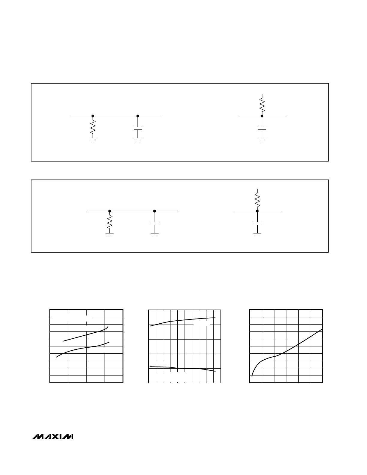
Figure 5. Shutdown Sequence

MAX1240/MAX1241
+2.7V, Low-Power,
12-Bit Serial ADCs in 8-Pin SO
10 ______________________________________________________________________________________
ed. After an internally timed conversion period, the end
of conversion is signaled by DOUT pulling high. Data
can then be shifted out serially with the external clock.
Using
SHDN
to Reduce Supply Current
Power consumption can be reduced significantly by
shutting down the MAX1240/MAX1241 between conversions. Figure 6 shows a plot of average supply current versus conversion rate. Because the MAX1241
uses an external reference voltage (assumed to be present continuously), it “wakes up” from shutdown more
quickly (in 4µs) and therefore provides lower average
supply currents. The wake-up time (t
WAKE
) is the time
from when SHDN is deasserted to the time when a conversion may be initiated (Figure 5). For the MAX1240,
this time depends on the time in shutdown (Figure 7)
because the external 4.7µF reference bypass capacitor
loses charge slowly during shutdown.
External Clock
The actual conversion does not require the external
clock. This allows the conversion result to be read back
at the µP’s convenience at any clock rate from up to
2.1MHz. The clock duty cycle is unrestricted if each
clock phase is at least 200ns. Do not run the clock
while a conversion is in progress.
Timing and Control
Conversion-start and data-read operations are controlled
by the CSand SCLK digital inputs. The timing diagrams
of Figures 8 and 9 outline serial-interface operation.
A CSfalling edge initiates a conversion sequence: the
T/H stage holds the input voltage, the ADC begins to
convert, and DOUT changes from high impedance to
logic low. SCLK must be kept low during the conversion. An internal register stores the data when the conversion is in progress.
10
1
0.01
0.001
0.1 1 10 100 1k 10k 100k
0.1
CONVERSION RATE (Hz)
SUPPLY CURRNET (mA)
V
DD
=
V
REF
= 3.0V
R
LOAD
= ∞, C
LOAD
= 50pF
CODE = 010101010000
MAX1241 FIG. 06a
MAX1241
MAX1240
Figure 6. Average Supply Current vs. Conversion Rate
1.0
0.0
0.001 0.01 0.1 1 10
0.8
0.6
0.4
0.2
TIME IN SHUTDOWN
(sec)
POWER-UP DELAY (ms)
MAX1240/41-07a
Figure 7. Typical Reference Power-Up Delay vs. Time in
Shutdown
EOC
INTERFACE IDLE
CONVERSION
IN PROGRESS
EOC
0µs
TRAILING
ZEROS
IDLE
CLOCK OUT SERIAL DATA
TRACK/HOLD
STATE
TRACK
HOLD
TRACK
DOUT B11 B10 B9 B8 B7 B6 B5 B4 B3 B2 B1 B0
SCLK
14 8 12 16
7.5µs (t
CONV
)
HOLD
0µs
(tCS)
TOTAL = 13.7µs
12.5 × 0.476µs = 5.95µs
CYCLE TIME
CS
0.24µs
Figure 8. Interface Timing Sequence
End of conversion (EOC) is signaled by DOUT going
high. DOUT’s rising edge can be used as a framing
signal. SCLK shifts the data out of this register any time
after the conversion is complete. DOUT transitions on
SCLK’s falling edge. The next falling clock edge produces the MSB of the conversion at DOUT, followed by
the remaining bits. Since there are 12 data bits and one
leading high bit, at least 13 falling clock edges are
needed to shift out these bits. Extra clock pulses occurring after the conversion result has been clocked out,
and prior to a rising edge of CS, produce trailing zeros
at DOUT and have no effect on converter operation.
Minimum cycle time is accomplished by using DOUT’s
rising edge as the EOC signal. Clock out the data with
12.5 clock cycles at full speed. Pull CShigh after read-
ing the conversion’s LSB. After the specified minimum
time (tCS), CScan be pulled low again to initiate the
next conversion.
Output Coding and Transfer Function
The data output from the MAX1240/MAX1241 is binary,
and Figure 10 depicts the nominal transfer function.
Code transitions occur halfway between successiveinteger LSB values. If V
REF
= +2.500V, then 1 LSB =
610µV or 2.500V/4096.
____________Applications Information
Connection to Standard Interfaces
The MAX1240/MAX1241 serial interface is fully compatible with SPI/QSPI and MICROWIRE standard serial
interfaces (Figure 11).
If a serial interface is available, set the CPU’s serial
interface in master mode so the CPU generates the serial clock. Choose a clock frequency up to 2.1MHz.
1) Use a general-purpose I/O line on the CPU to pull
CS
low. Keep SCLK low.
2) Wait the for the maximum conversion time specified
before activating SCLK. Alternatively, look for a DOUT
rising edge to determine the end of conversion.
3) Activate SCLK for a minimum of 13 clock cycles. The
first falling clock edge produces the MSB of the
DOUT conversion. DOUT output data transitions on
SCLK’s falling edge and is available in MSB-first format. Observe the SCLK to DOUT valid timing characteristic. Data can be clocked into the µP on
SCLK’s rising edge.
4) Pull CShigh at or after the 13th falling clock edge. If
CS
remains low, trailing zeros are clocked out after
the LSB.
MAX1240/MAX1241
+2.7V, Low-Power,
12-Bit Serial ADCs in 8-Pin SO
______________________________________________________________________________________ 11
11…111
11…110
11…101
00…011
00…010
00…001
00…000
012 FS
OUTPUT CODE
FS - 3/2LSBINPUT VOLTAGE (LSBs)
FS = V
REF
- 1LSB
1LSB =
V
REF
4096
FULL-SCALE
TRANSITION
3
Figure 10. Unipolar Transfer Function, Full Scale (FS) = V
REF
-
1LSB, Zero Scale (ZS) = GND
Figure 9. Detailed Serial-Interface Timing
CS
t
CS0
SCLK
t
DV
DOUT
INTERNAL
(TRACK/ACQUIRE)
T/H
t
APR
t
CONV
(HOLD) (TRACK/ACQUIRE)
t
CS
…
t
CH
…
t
DO
…
t
STR
t
CL
B2 B1 B0
t
TR
…

MAX1240/MAX1241
+2.7V, Low-Power,
12-Bit Serial ADCs in 8-Pin SO
12 ______________________________________________________________________________________
5) With CS = high, wait the minimum specified time, tCS,
before initiating a new conversion by pulling CS low.
If a conversion is aborted by pulling CS high before
the conversion’s end, wait for the minimum acquisition time, t
ACQ
, before starting a new conversion.
CS must be held low until all data bits are clocked out.
Data can be output in two bytes or continuously, as
shown in Figure 8. The bytes contain the result of the
conversion padded with one leading 1, and trailing 0s.
SPI and MICROWIRE
When using SPI or MICROWIRE, set CPOL = 0 and
CPHA = 0. Conversion begins with a CSfalling edge.
DOUT goes low, indicating a conversion in progress. Wait
until DOUT goes high or until the maximum specified
7.5µs conversion time elapses. Two consecutive 1-byte
reads are required to get the full 12 bits from the ADC.
DOUT output data transitions on SCLK’s falling edge and
is clocked into the µP on SCLK’s rising edge.
The first byte contains a leading 1, and seven bits of conversion result. The second byte contains the remaining
five bits and three trailing zeros. See Figure 11 for connections and Figure 12 for timing.
QSPI
Set CPOL = CPHA = 0. Unlike SPI, which requires two
1-byte reads to acquire the 12 bits of data from the ADC,
QSPI allows the minimum number of clock cycles necessary to clock in the data. The MAX1240/MAX1241
requires 13 clock cycles from the µP to clock out the 12
bits of data with no trailing zeros (Figure 13). The maximum clock frequency to ensure compatibility with QSPI is
2.097MHz.
Layout, Grounding, and Bypassing
For best performance, use printed circuit boards. Wirewrap boards are not recommended. Board layout should
ensure that digital and analog signal lines are separated
from each other. Do not run analog and digital (especially
clock) lines parallel to one another, or digital lines underneath the ADC package.
Figure 14 shows the recommended system ground connections. Establish a single-point analog ground (“star”
ground point) at GND, separate from the logic ground.
Connect all other analog grounds and DGND to this star
ground point for further noise reduction. No other digital
system ground should be connected to this single-point
analog ground. The ground return to the power supply for
this ground should be low impedance and as short as
possible for noise-free operation.
High-frequency noise in the V
DD
power supply may affect
the ADC’s high-speed comparator. Bypass this supply to
the single-point analog ground with 0.1µF and 4.7µF
bypass capacitors. Minimize capacitor lead lengths for
best supply-noise rejection. If the power supply is very
noisy, a 10Ω resistor can be connected as a lowpass filter
to attenuate supply noise (Figure 14).
CS
SCLK
DOUT
I/O
SCK
MISO
+3V
SS
a) SPI
CS
SCLK
DOUT
CS
SCK
MISO
+3V
SS
b) QSPI
MAX1240
MAX1241
MAX1240
MAX1241
MAX1240
MAX1241
CS
SCLK
DOUT
I/O
SK
SI
c) MICROWIRE
Figure 11. Common Serial-Interface Connections to the
MAX1241

MAX1240/MAX1241
+2.7V, Low-Power,
12-Bit Serial ADCs in 8-Pin SO
______________________________________________________________________________________ 13
HIGH-Z
D11 D10 D9 D8 D7 D6 D5 D4 D3 D2 D1 D0
t
CONV
DOUT*
CS
SCLK
1ST BYTE READ 2ND BYTE READ
EOC
MSB LSB
*WHEN CS IS HIGH, DOUT = HIGH -Z
Figure 12. SPI/MICROWIRE Serial Interface Timing (CPOL = CPHA = 0)
Figure 13. QSPI Serial Interface Timing (CPOL = CPHA = 0)
SUPPLIES
+3V +3V GND
DGND+3V
DIGITAL
CIRCUITRY
GNDV
DD
MAX1240
MAX1241
*OPTIONAL
R* = 10Ω
4.7µF
0.1µF
Figure 14. Power-Supply Grounding Condition
SCLK
CS
t
CONV
DOUT*
D11 D10 D9 D8 D7 D6 D5 D4 D3 D2 D1 D0
MSB LSB
HIGH-Z
*WHEN CS IS HIGH, DOUT = HIGH -Z
EOC

MAX1240/MAX1241
+2.7V, Low-Power,
12-Bit Serial ADCs in 8-Pin SO
14 ______________________________________________________________________________________
PART
MAX1240AEPA
MAX1240BESA
MAX1240BMJA -55°C to +125°C
-40°C to +85°C
-40°C to +85°C
TEMP. RANGE
PIN-
PACKAGE
8 Plastic DIP
8 SO
8 CERDIP**
MAX1241AEPA -40°C to +85°C 8 Plastic DIP ±1/2
MAX1241BEPA -40°C to +85°C 8 Plastic DIP ±1
MAX1241AESA -40°C to +85°C 8 SO ±1/2
MAX1241BESA -40°C to +85°C 8 SO
INL
(LSB)
±1/2
±1
±1
±1
MAX1241AMJA -55°C to +125°C 8 CERDIP** ±1/2
MAX1241BMJA -55°C to +125°C 8 CERDIP** ±1
MAX1240AMJA -55°C to +125°C 8 CERDIP** ±1/2
MAX1241BC/D 0°C to +70°C Dice* ±1
*
Dice are specified at TA= +25°C, DC parameters only.
**
Contact factory for availability and processing to MIL-STD-883.
__Ordering Information (continued)
___________________Chip Information
TRANSISTOR COUNT: 2558
SUBSTRATE CONNECTED TO GND
MAX1241ACPA
MAX1241BCPA
MAX1241BCSA 0°C to +70°C
0°C to +70°C
0°C to +70°C 8 Plastic DIP
8 Plastic DIP
8 SO
±1/2
±1
±1
MAX1241ACSA 0°C to +70°C 8 SO ±1/2
MAX1240AESA
-40°C to +85°C 8 SO ±1/2
MAX1240BEPA
-40°C to +85°C 8 Plastic DIP ±1
MAX1240CEPA
-40°C to +85°C 8 Plastic DIP ±1
MAX1240CESA
-40°C to +85°C 8 SO ±1
MAX1240CMJA -55°C to +125°C 8 CERDIP** ±1
MAX1241CCPA 0°C to +70°C 8 Plastic DIP ±1
MAX1241CCSA 0°C to +70°C 8 SO ±1
MAX1241CEPA -40°C to +85°C 8 Plastic DIP ±1
MAX1241CESA -40°C to +85°C 8 SO ±1
MAX1241CMJA -55°C to +125°C 8 CERDIP** ±1

SOICN.EPS
MAX1240/MAX1241
+2.7V, Low-Power,
12-Bit Serial ADCs in 8-Pin SO
______________________________________________________________________________________ 15
________________________________________________________Package Information
PDIPN.EPS

MAX1240/MAX1241
+2.7V, Low-Power,
12-Bit Serial ADCs in 8-Pin SO
Maxim cannot assume responsibility for use of any circuitry other than circuitry entirely embodied in a Maxim product. No circuit patent licenses are
implied. Maxim reserves the right to change the circuitry and specifications without notice at any time.
16
____________________Maxim Integrated Products, 120 San Gabriel Drive, Sunnyvale, CA 94086 408-737-7600
© 1998 Maxim Integrated Products Printed USA is a registered trademark of Maxim Integrated Products.
___________________________________________Package Information (continued)
CDIPS.EPS
 Loading...