

Page 1
General Description
The MAX1236–MAX1239 low-power, 12-bit, multichannel analog-to-digital converters (ADCs) feature internal
track/hold (T/H), voltage reference, clock, and an
I2C-compatible 2-wire serial interface. These devices
operate from a single supply of 2.7V to 3.6V (MAX1237/
MAX1239) or 4.5V to 5.5V (MAX1236/MAX1238) and
require only 670µA at the maximum sampling rate of
94.4ksps. Supply current falls below 230µA for sampling rates under 46ksps. AutoShutdown™ powers
down the devices between conversions, reducing supply current to less than 1µA at low throughput rates.
The MAX1236/MAX1237 have four analog input channels each, while the MAX1238/MAX1239 have 12 analog input channels each. The fully differential analog
inputs are software configurable for unipolar or bipolar,
and single-ended or differential operation.
The full-scale analog input range is determined by the
internal reference or by an externally applied reference
voltage ranging from 1V to VDD. The MAX1237/
MAX1239 feature a 2.048V internal reference and the
MAX1236/MAX1238 feature a 4.096V internal reference.
The MAX1236/MAX1237 are available in an 8-pin µMAX
®
package. The MAX1238/MAX1239 are available in a 16pin QSOP package. The MAX1236–MAX1239 are guaranteed over the extended temperature range
(-40°C to +85°C). For pin-compatible 10-bit parts, refer to
the MAX1136–MAX1139 data sheet. For pin-compatible
8-bit parts, refer to the MAX1036–MAX1039 data sheet.
Applications
Features
♦ High-Speed I2C-Compatible Serial Interface
400kHz Fast Mode
1.7MHz High-Speed Mode
♦ Single-Supply
2.7V to 3.6V (MAX1237/MAX1239)
4.5V to 5.5V (MAX1236/MAX1238)
♦ Internal Reference
2.048V (MAX1237/MAX1239)
4.096V (MAX1236/MAX1238)
♦ External Reference: 1V to V
DD
♦ Internal Clock
♦ 4-Channel Single-Ended or 2-Channel Fully
Differential (MAX1236/MAX1237)
♦ 12-Channel Single-Ended or 6-Channel Fully
Differential (MAX1238/MAX1239)
♦ Internal FIFO with Channel-Scan Mode
♦ Low Power
670µA at 94.4ksps
230µA at 40ksps
60µA at 10ksps
6µA at 1ksps
0.5µA in Power-Down Mode
♦ Software-Configurable Unipolar/Bipolar
♦ Small Packages
8-Pin µMAX (MAX1236/MAX1237)
16-Pin QSOP (MAX1238/MAX1239)
MAX1236–MAX1239
2.7V to 3.6V and 4.5V to 5.5V, Low-Power,
4-/12-Channel, 2-Wire Serial, 12-Bit ADCs
________________________________________________________________ Maxim Integrated Products 1
Ordering Information
19-2333; Rev 4; 9/06
For pricing, delivery, and ordering information, please contact Maxim/Dallas Direct! at
1-888-629-4642, or visit Maxim’s website at www.maxim-ic.com.
PART
TEMP RANGE
PIN-
I2C SLAVE
ADDRESS
MAX1236EUA
8 µMAX 0110100
MAX1236KEUA
8 µMAX 0110000
MAX1236LEUA
8 µMAX 0110010
MAX1236MEUA
8 µMAX 0110110
MAX1237EUA
8 µMAX 0110100
MAX1237KEUA
8 µMAX 0110000
MAX1237LEUA
8 µMAX 0110010
MAX1237MEUA
8 µMAX 0110110
MAX1238EEE
0110101
MAX1238KEEE
0110001
MAX1238LEEE
0110011
MAX1238MEEE
0110111
Pin Configurations and Typical Operating Circuit appear at
end of data sheet.
AutoShutdown is a trademark of Maxim Integrated Products, Inc.
µMAX is a registered trademark of Maxim Integrated Products, Inc.
Ordering Information continued at end of data sheet.
PART
INPUT
INTERNAL
REFERENCE
(V)
SUPPLY
VOLTAGE
(V)
INL
(LSB)
MAX1236
4 4.096
±1
MAX1237
4 2.048
±1
MAX1238
12 4.096
±1
MAX1239
12 2.048
±1
Hand-Held Portable
Applications
Medical Instruments
Battery-Powered Test
Equipment
Solar-Powered Remote
Systems
Received-Signal-Strength
Indicators
System Supervision
Selector Guide
CHANNELS
4.5 to 5.5
2.7 to 3.6
4.5 to 5.5
2.7 to 3.6
PACKAGE
-40°C to +85°C
-40°C to +85°C
-40°C to +85°C
-40°C to +85°C
-40°C to +85°C
-40°C to +85°C
-40°C to +85°C
-40°C to +85°C
-40°C to +85°C 16 QSOP
-40°C to +85°C 16 QSOP
-40°C to +85°C 16 QSOP
-40°C to +85°C 16 QSOP
Page 2
MAX1236–MAX1239
2.7V to 3.6V and 4.5V to 5.5V, Low-Power,
4-/12-Channel, 2-Wire Serial, 12-Bit ADCs
2 _______________________________________________________________________________________
ABSOLUTE MAXIMUM RATINGS
ELECTRICAL CHARACTERISTICS
(VDD= 2.7V to 3.6V (MAX1237/MAX1239), VDD= 4.5V to 5.5V (MAX1236/MAX1238), V
REF
= 2.048V (MAX1237/MAX1239), V
REF
=
4.096V (MAX1236/MAX1238), C
REF
= 0.1µF, f
SCL
= 1.7MHz, TA= T
MIN
to T
MAX
, unless otherwise noted. Typical values are at
T
A
= +25°C, see Tables 1–5 for programming notation.)
Stresses beyond those listed under “Absolute Maximum Ratings” may cause permanent damage to the device. These are stress ratings only, and functional
operation of the device at these or any other conditions beyond those indicated in the operational sections of the specifications is not implied. Exposure to
absolute maximum rating conditions for extended periods may affect device reliability.
VDDto GND..............................................................-0.3V to +6V
AIN0–AIN11,
REF to GND............-0.3V to the lower of (VDD+ 0.3V) and 6V
SDA, SCL to GND.....................................................-0.3V to +6V
Maximum Current Into Any Pin .........................................±50mA
Continuous Power Dissipation (TA= +70°C)
8-Pin µMAX (derate 4.5mW/°C above +70°C) .............362mW
16-Pin QSOP (derate 8.3mW/°C above +70°C)........666.7mW
Operating Temperature Range ...........................-40°C to +85°C
Junction Temperature......................................................+150°C
Storage Temperature Range .............................-60°C to +150°C
Lead Temperature (soldering, 10s) .................................+300°C
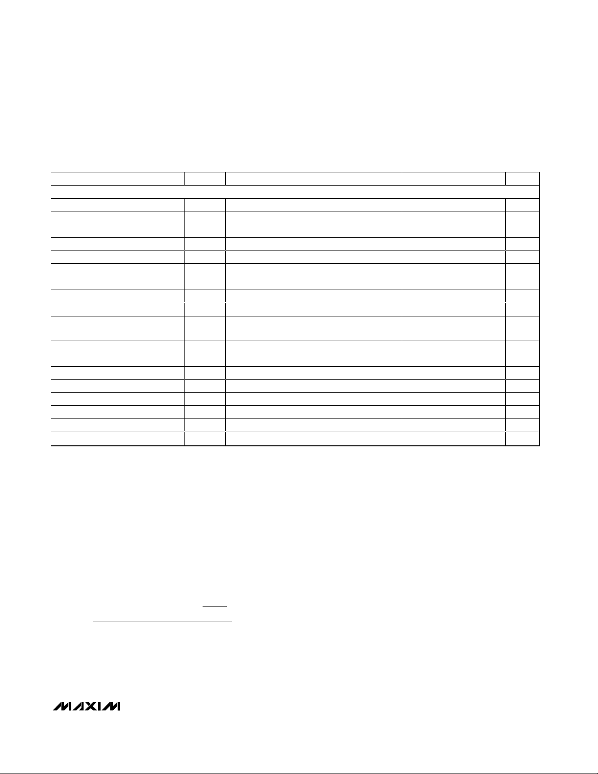
PARAMETER
CONDITIONS
UNITS
DC ACCURACY (Note 1)
Resolution 12 Bits
Relative Accuracy INL (Note 2) ±1
LSB
Differential Nonlinearity DNL No missing codes over temperature ±1
LSB
Offset Error ±4
LSB
Offset-Error Temperature
Coefficient
Relative to FSR 0.3
ppm/°C
Gain Error (Note 3) ±4
LSB
Gain-Temperature Coefficient Relative to FSR 0.3
ppm/°C
Channel-to-Channel Offset
Matching
LSB
Channel-to-Channel Gain
Matching
LSB
DYNAMIC PERFORMANCE (f
IN(SINE-WAVE)
= 10kHz, V
IN(P-P)
= V
REF
, f
SAMPLE
= 94.4ksps)
Signal-to-Noise Plus Distortion
70 dB
Total Harmonic Distortion THD Up to the 5th harmonic -78 dB
Spurious-Free Dynamic Range SFDR 78 dB
Full-Power Bandwidth SINAD > 68dB 3
MHz
Full-Linear Bandwidth -3dB point 5
MHz
CONVERSION RATE
Internal clock 7.5
Conversion Time (Note 4)
External clock
µs
SYMBOL
MIN TYP MAX
SINAD
t
CONV
10.6
±0.1
±0.1
Page 3
MAX1236–MAX1239
2.7V to 3.6V and 4.5V to 5.5V, Low-Power,
4-/12-Channel, 2-Wire Serial, 12-Bit ADCs
_______________________________________________________________________________________ 3
ELECTRICAL CHARACTERISTICS (continued)
(VDD= 2.7V to 3.6V (MAX1237/MAX1239), VDD= 4.5V to 5.5V (MAX1236/MAX1238), V
REF
= 2.048V (MAX1237/MAX1239), V
REF
=
4.096V (MAX1236/MAX1238), C
REF
= 0.1µF, f
SCL
= 1.7MHz, TA= T
MIN
to T
MAX
, unless otherwise noted. Typical values are at
T
A
= +25°C, see Tables 1–5 for programming notation.)
PARAMETER
CONDITIONS
UNITS
Internal clock, SCAN[1:0] = 01 51
Internal clock, SCAN[1:0] = 00
CS[3:0] = 1011 (MAX1238/MAX1239)
51
Throughput Rate
External clock
ksps
Track/Hold Acquisition Time
ns
Internal Clock Frequency 2.8
MHz
External clock, fast mode 60
Aperture Delay (Note 5) t
AD
External clock, high-speed mode 30
ns
ANALOG INPUT (AIN0–AIN11)
Unipolar 0
Input-Voltage Range, SingleEnded and Differential (Note 6)
Bipolar 0
V
Input Multiplexer Leakage Current
ON/OFF leakage current, V
AIN
_ = 0 or V
DD
±1µA
Input Capacitance C
IN
22 pF
INTERNAL REFERENCE (Note 7)
MAX1237/MAX1239
Reference Voltage V
REF
TA = +25°C
MAX1236/MAX1238
V
Reference-Voltage Temperature
Coefficient
25
ppm/°C
REF Short-Circuit Current 2mA
REF Source Impedance 1.5 kΩ
EXTERNAL REFERENCE
REF Input-Voltage Range V
REF
(Note 8) 1
V
REF Input Current I
REF
f
SAMPLE
= 94.4ksps 40 µA
DIGITAL INPUTS/OUTPUTS (SCL, SDA)
Input-High Voltage V
IH
V
Input-Low Voltage V
IL
V
Input Hysteresis
V
Input Current I
IN
VIN = 0 to V
DD
±10 µA
Input Capacitance C
IN
15 pF
Output Low Voltage V
OL
I
SINK
= 3mA 0.4 V
SYMBOL
f
SAMPLE
TCV
V
HYST
REF
MIN TYP MAX
94.4
800
±0.01
1.968 2.048 2.128
3.936 4.096 4.256
0.7 ✕ V
DD
0.1 ✕ V
DD
0.3 ✕ V
V
REF
±V
/2
REF
V
DD
DD
Page 4
MAX1236–MAX1239
2.7V to 3.6V and 4.5V to 5.5V, Low-Power,
4-/12-Channel, 2-Wire Serial, 12-Bit ADCs
4 _______________________________________________________________________________________
ELECTRICAL CHARACTERISTICS (continued)
(VDD= 2.7V to 3.6V (MAX1237/MAX1239), VDD= 4.5V to 5.5V (MAX1236/MAX1238), V
REF
= 2.048V (MAX1237/MAX1239), V
REF
=
4.096V (MAX1236/MAX1238), C
REF
= 0.1µF, f
SCL
= 1.7MHz, TA= T
MIN
to T
MAX
, unless otherwise noted. Typical values are at
T
A
= +25°C, see Tables 1–5 for programming notation.)
PARAMETER
CONDITIONS
UNITS
POWER REQUIREMENTS
MAX1237/MAX1239 2.7 3.6
Supply Voltage V
DD
MAX1236/MAX1238 4.5 5.5
V
Internal reference
f
SAMPLE
= 94.4ksps
external clock
External reference
900
Internal reference
f
SAMPLE
= 40ksps
internal clock
External reference
Internal reference
f
SAMPLE
= 10ksps
internal clock
External reference 60
Internal reference
f
SAMPLE
=1ksps
internal clock
External reference 6
Supply Current I
DD
Shutdown (internal REF off) 0.5 10
µA
Power-Supply Rejection Ratio PSRR Full-scale input (Note 9)
LSB/V
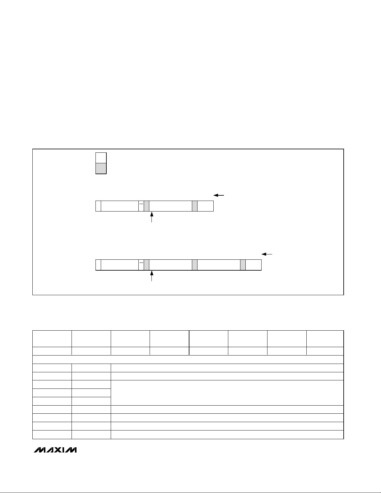
TIMING CHARACTERISTICS (Figure 1)
(VDD= 2.7V to 3.6V (MAX1237/MAX1239), VDD= 4.5V to 5.5V (MAX1236/MAX1238), V
REF
= 2.048V (MAX1237/MAX1239), V
REF
=
4.096V (MAX1236/MAX1238), C
REF
= 0.1µF, f
SCL
= 1.7MHz, TA= T
MIN
to T
MAX
, unless otherwise noted. Typical values are at
T
A
= +25°C, see Tables 1–5 for programming notation.)
PARAMETER
CONDITIONS
UNITS
TIMING CHARACTERISTICS FOR FAST MODE
Serial-Clock Frequency f
SCL
400 kHz
Bus Free Time Between a STOP (P)
and a START (S) Condition
t
BUF
1.3 µs
Hold Time for START (S) Condition
,
0.6 µs
Low Period of the SCL Clock t
LOW
1.3 µs
High Period of the SCL Clock t
HIGH
0.6 µs
Setup Time for a Repeated START
Condition (Sr)
,
0.6 µs
Data Hold Time (Note 10)
,
0 900 ns
Data Setup Time
,
ns
Rise Time of Both SDA and SCL
Signals, Receiving
t
R
Measured from 0.3VDD - 0.7V
DD
300 ns
Fall Time of SDA Transmitting t
F
Measured from 0.3VDD - 0.7V
DD
300 ns
Setup Time for STOP (P) Condition
,
0.6 µs
Capacitive Load for Each Bus Line
C
B
400 pF
Pulse Width of Spike Suppressed
t
SP
50 ns
SYMBOL
MIN TYP MAX
900 1150
670
530
230
380
330
±0.5 ±0.2
SYMBOL
t
HD
STA
t
SU
STA
t
HD
DAT
t
SU
DAT
t
SU
STO
MIN TYP MAX
100
20 + 0.1C
B
20 + 0.1C
B
Page 5
MAX1236–MAX1239
2.7V to 3.6V and 4.5V to 5.5V, Low-Power,
4-/12-Channel, 2-Wire Serial, 12-Bit ADCs
_______________________________________________________________________________________ 5
PARAMETER
SYMBOL
CONDITIONS
MIN
TYP
MAX
UNITS
TIMING CHARACTERISTICS FOR HIGH-SPEED MODE (CB = 400pF, Note 11)
Serial Clock Frequency
(Note 12) 1.7
MHz
Hold Time, Repeated START
Condition (Sr)
,
ns
Low Period of the SCL Clock t
LOW
ns
High Period of the SCL Clock t
HIGH
ns
Setup Time for a Repeated START
Condition (Sr)
ns
Data Hold Time
(Note 10) 0 150 ns
Data Setup Time
10 ns
Rise Time of SCL Signal
(Current Source Enabled)
t
RCL
20 80 ns
Rise Time of SCL Signal after
Acknowledge Bit
t
RCL1
Measured from 0.3VDD - 0.7V
DD
20 160 ns
Fall Time of SCL Signal t
FCL
Measured from 0.3VDD - 0.7V
DD
20 80 ns
Rise Time of SDA Signal t
RDA
Measured from 0.3VDD - 0.7V
DD
20 160 ns
Fall Time of SDA Signal t
FDA
Measured from 0.3VDD - 0.7V
DD
20 160 ns
Setup Time for STOP (P) Condition
ns
Capacitive Load for Each Bus Line
C
B
400 pF
Pulse Width of Spike Suppressed
t
SP
(Notes 10 and 12) 0 10 ns
TIMING CHARACTERISTICS (Figure 1) (continued)
(VDD= 2.7V to 3.6V (MAX1237/MAX1239), VDD= 4.5V to 5.5V (MAX1236/MAX1238), V
REF
= 2.048V (MAX1237/MAX1239), V
REF
=
4.096V (MAX1236/MAX1238), C
REF
= 0.1µF, f
SCL
= 1.7MHz, TA= T
MIN
to T
MAX
, unless otherwise noted. Typical values are at
T
A
= +25°C, see Tables 1–5 for programming notation.)
Note 1: For DC accuracy, the MAX1136/MAX1138 are tested at V
DD
= 5V and the MAX1137/MAX1139 are tested at VDD= 3V. All
devices are configured for unipolar, single-ended inputs.
Note 2: Relative accuracy is the deviation of the analog value at any code from its theoretical value after the full-scale range and
offsets have been calibrated.
Note 3: Offset nulled.
Note 4: Conversion time is defined as the number of clock cycles needed for conversion multiplied by the clock period. Conversion
time does not include acquisition time. SCL is the conversion clock in the external clock mode.
Note 5: A filter on the SDA and SCL inputs suppresses noise spikes and delays the sampling instant.
Note 6: The absolute input-voltage range for the analog inputs (AIN0–AIN11) is from GND to V
DD
.
Note 7: When the internal reference is configured to be available at AIN_/REF (SEL[2:1] = 11) decouple AIN_/REF to GND with a
0.01µF capacitor.
Note 8: ADC performance is limited by the converter’s noise floor, typically 300µV
P-P
.
Note 9: Measured as for the MAX1237/MAX1239
VVVV
V
VV
FS FS
REF
N
(. ) (. )
(. . )
36 27
21
36 27
−
−
−
[]
×
f
SCLH
t
HD
STA
tSU,
STA
tHD,
DAT
tSU,
DAT
tSU,
STO
160
320
120
160
160
Page 6
MAX1236–MAX1239
2.7V to 3.6V and 4.5V to 5.5V, Low-Power,
4-/12-Channel, 2-Wire Serial, 12-Bit ADCs
6 _______________________________________________________________________________________
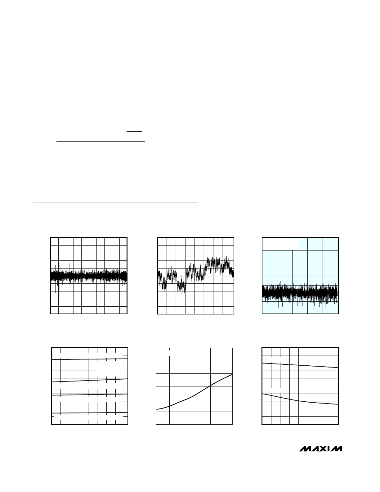
Typical Operating Characteristics
(VDD= 3.3V (MAX1237/MAX1239), VDD= 5V (MAX1236/MAX1238), f
SCL
= 1.7MHz, (50% duty cycle), f
SAMPLE
= 94.4ksps, single-
ended, unipolar, TA= +25°C, unless otherwise noted.)
-0.5
-0.2
-0.4
-0.3
0.2
0.1
0.1
0
0.3
0.5
0 4000
DIFFERENTIAL NONLINEARITY
vs. DIGITAL CODE
MAX1236 toc01
DIGITAL OUTPUT CODE
DNL (LSB)
1000 1500500
2000 2500
3000 3500
0.4
-1.0
-0.4
-0.6
-0.8
-0.2
0
0.2
0.4
0.6
0.8
1.0
INTEGRAL NONLINEARITY
vs. DIGITAL CODE
MAX1236 toc02
DIGITAL OUTPUT CODE
INL (LSB)
04000
1000 1500500
2000 2500
3000 3500
-180
-160
-140
-120
-100
-80
-60
0 10k 20k 30k 40k 50k
FFT PLOT
MAX1236 toc03
FREQUENCY (Hz)
AMPLITUDE (dBc)
f
SAMPLE
= 94.4ksps
f
IN
= 10kHz
300
400
350
500
450
600
550
650
750
700
800
-40 -10 5-25 20 35 50 65 80
SUPPLY CURRENT vs. TEMPERATURE
(MAX1238/MAX1239)
MAX1236 toc04
TEMPERATURE (°C)
SUPPLY CURRENT (µA)
INTERNAL REFERENCE MAX1239/MAX1237
INTERNAL REFERENCE MAX1238/MAX1236
EXTERNAL REFERENCE MAX1238/MAX1236
EXTERNAL REFERENCE MAX1239/MAX1237
SETUP BYTE
EXT REF: 10111011
INT REF: 11011011
0
0.2
0.1
0.4
0.3
0.5
0.6
2.7 5.2
SHUTDOWN SUPPLY CURRENT
vs. SUPPLY VOLTAGE
MAX1236 toc05
INPUT VOLTAGE (V)
I
DD
(µA)
3.73.2 4.2 4.7
SDA = SCL = V
DD
0
0.10
0.05
0.20
0.15
0.30
0.25
0.35
0.45
0.40
0.50
-40 -10 5
-25
20 35 50 65 80
SHUTDOWN SUPPLY CURRENT
vs. TEMPERATURE
MAX1236 toc06
TEMPERATURE (°C)
SUPPLY CURRENT (µA)
MAX1238
MAX1239
and for the MAX1236/MAX1238 where N is the number of bits and V
REF
.
Note 10: A master device must provide a data hold time for SDA (referred to V
IL
of SCL) in order to bridge the undefined region of
SCL’s falling edge (see Figure 1).
Note 11: C
B
= total capacitance of one bus line in pF.
Note 12: f
SCL
must meet the minimum clock low time plus the rise/fall times.
VVVV
V
VV
FS FS
REF
N
(. ) (. )
(. . )
55 45
21
55 45
−
−
−
[]
×
TIMING CHARACTERISTICS (Figure 1) (continued)
(VDD= 2.7V to 3.6V (MAX1237/MAX1239), VDD= 4.5V to 5.5V (MAX1236/MAX1238), V
REF
= 2.048V (MAX1237/MAX1239), V
REF
=
4.096V (MAX1236/MAX1238), C
REF
= 0.1µF, f
SCL
= 1.7MHz, TA= T
MIN
to T
MAX
, unless otherwise noted. Typical values are at
T
A
= +25°C, see Tables 1–5 for programming notation.)
Page 7
MAX1236–MAX1239
2.7V to 3.6V and 4.5V to 5.5V, Low-Power,
4-/12-Channel, 2-Wire Serial, 12-Bit ADCs
_______________________________________________________________________________________ 7
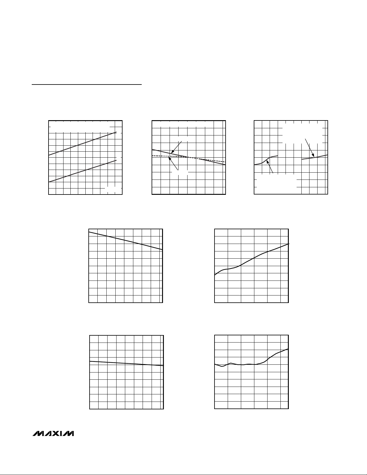
200
300
250
350
400
450
500
550
600
650
700
750
800
02030406080100
AVERAGE SUPPLY CURRENT vs.
CONVERSION RATE (EXTERNAL CLOCK)
MAX1236 toc07
CONVERSION RATE (ksps)
AVERAGE I
DD
(µA)
010 50 70 90
A
B
A) INTERNAL REFERENCE ALWAYS ON
B) EXTERNAL REFERENCE
MAX1238
0.9990
0.9994
0.9992
0.9998
0.9996
1.0002
1.0000
1.0004
1.0008
1.0006
1.0010
-40 -10 5-25 20 35 50 65 80
INTERNAL REFERENCE VOLTAGE
vs. TEMPERATURE
MAX1236 toc08
TEMPERATURE (°C)
V
REF
NORMALIZED
NORMALIZED TO VALUE AT +25°C
MAX1238
MAX1239
0.99990
0.99994
0.99992
0.99998
0.99996
1.00002
1.00000
1.00004
1.00008
1.00006
1.00010
2.7 3.3 3.6 3.93.0 4.2 4.5 4.8 5.1 5.4
NORMALIZED REFERENCE VOLTAGE
vs. SUPPLY VOLTAGE
MAX1236 toc09
VDD (V)
V
REF
(V)
MAX1236/MAX1238
NORMALIZED TO
REFERENCE VALUE AT
V
DD
= 5V
MAX1237/MAX1239
NORMALIZED TO
REFERENCE VALUE AT
V
DD
= 3.3V
Typical Operating Characteristics (continued)
(VDD= 3.3V (MAX1237/MAX1239), VDD= 5V (MAX1236/MAX1238), f
SCL
= 1.7MHz, (50% duty cycle), f
SAMPLE
= 94.4ksps, single-
ended, unipolar, TA= +25°C, unless otherwise noted.)
OFFSET ERROR vs. TEMPERATURE
MAX1236 toc10
TEMPERATURE (°C)
OFFSET ERROR (LSB)
806535 50-10 5 20-25
-0.9
-0.8
-0.7
-0.6
-0.5
-0.4
-0.3
-0.2
-0.1
0
-1.0
-40
OFFSET ERROR vs. SUPPLY VOLTAGE
MAX1236 toc11
VDD (V)
OFFSET ERROR (LSB)
5.2 5.54.74.23.73.2
-1.6
-1.2
-0.8
-0.4
0
0.4
0.8
1.2
1.6
2.0
-2.0
2.7
GAIN ERROR vs. TEMPERATURE
MAX1236 toc12
TEMPERATURE (°C)
GAIN ERROR (LSB)
806535 50-10 5 20-25
0.2
0.4
0.6
0.8
1.0
1.2
1.4
1.6
1.8
2.0
0
-40
GAIN ERROR vs. SUPPLY VOLTAGE
MAX1236 toc13
VDD (V)
GAIN ERROR (LSB)
5.2 5.54.74.23.73.2
-1.6
-1.2
-0.8
-0.4
0
0.4
0.8
1.2
1.6
2.0
-2.0
2.7
Page 8

MAX1236–MAX1239
2.7V to 3.6V and 4.5V to 5.5V, Low-Power,
4-/12-Channel, 2-Wire Serial, 12-Bit ADCs
8 _______________________________________________________________________________________
Pin Description
PIN
MAX1236
MAX1237
MAX1238
MAX1239
NAME DESCRIPTION
1, 2, 3 1, 2, 3 AIN0–AIN2
— 4–8 AIN3–AIN7
— 16, 15, 14 AIN8–AIN10
Analog Inputs
4—AIN3/REF
Analog Input 3/Reference Input or Output. Selected in the setup
register (see Tables 1 and 6).
—13AIN11/REF
Analog Input 11/Reference Input or Output. Selected in the setup
register (see Tables 1 and 6).
59SCL Clock Input
610SDA Data Input/Output
711GND Ground
812VDDPositive Supply. Bypass to GND with a 0.1µF capacitor.
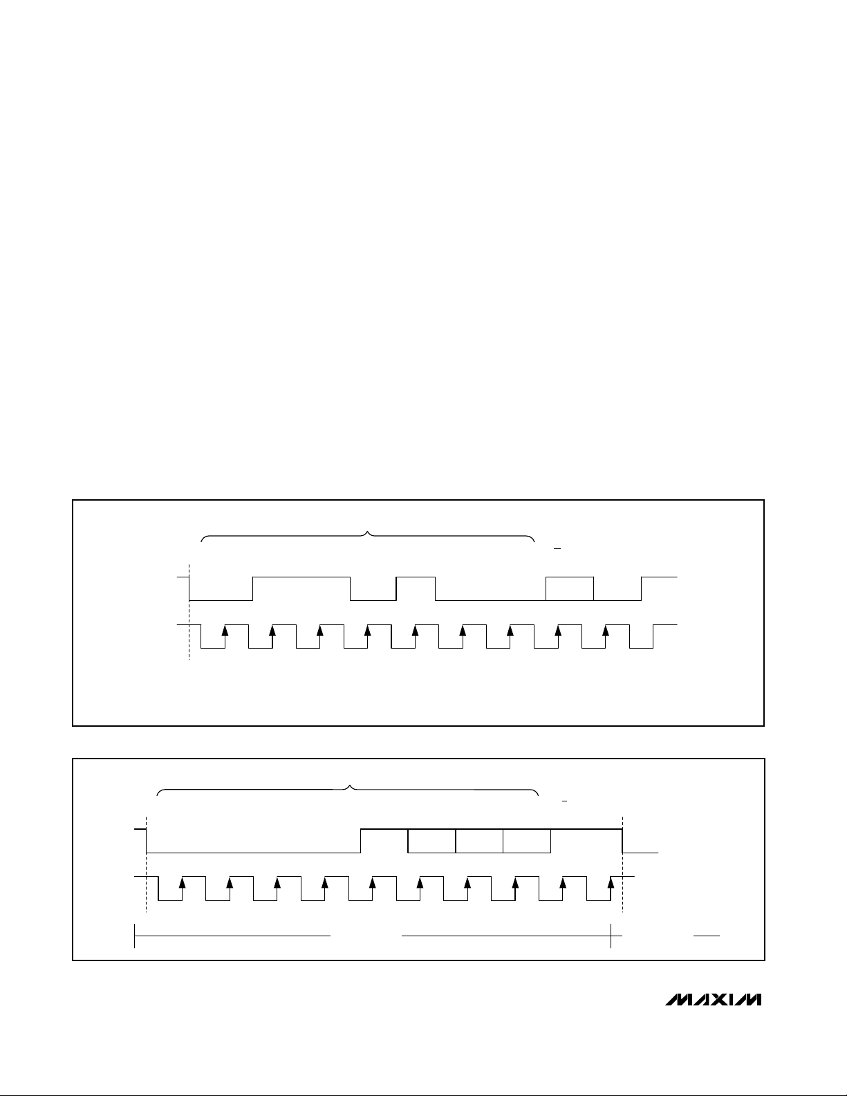
Figure 1. 2-Wire Serial Interface Timing
A. F/S-MODE 2-WIRE SERIAL INTERFACE TIMING
SDA
t
t
SCL
t
HD.STA
S
B. HS-MODE 2-WIRE SERIAL INTERFACE TIMING
SDA
t
SCL
t
HD.STA
S Sr A
SU.DAT
LOW
t
HIGH
t
R
t
LOW
SU.DAT
t
HIGH
t
RCL
t
HD.DAT
t
F
t
HD.DAT
t
FCL
t
SU.STA
t
SU.STA
t
HD.STA
Sr
t
HD.STA
A
t
RCL1
HS-MODE F/S-MODE
t
SU.STO
t
SU.STO
t
R
PS
t
RDA
P
t
t
F
t
BUF
t
FDA
t
BUF
S
Page 9

Detailed Description
The MAX1236–MAX1239 analog-to-digital converters
(ADCs) use successive-approximation conversion techniques and fully differential input track/hold (T/H) circuitry to capture and convert an analog signal to a
serial 12-bit digital output. The MAX1236/MAX1237 are
4-channel ADCs, and the MAX1238/MAX1239 are 12channel ADCs. These devices feature a high-speed, 2wire serial interface supporting data rates up to 1.7MHz.
Figure 2 shows the simplified internal structure for the
MAX1238/MAX1239.
Power Supply
The MAX1236–MAX1239 operates from a single supply
and consumes 670µA (typ) at sampling rates up to
94.4ksps. The MAX1237/MAX1239 feature a 2.048V
internal reference and the MAX1236/MAX1238 feature
a 4.096V internal reference. All devices can be configured for use with an external reference from 1V to V
DD
.
Analog Input and Track/Hold
The MAX1236–MAX1239 analog-input architecture contains an analog-input multiplexer (mux), a fully differential track-and-hold (T/H) capacitor, T/H switches, a
comparator, and a fully differential switched capacitive
digital-to-analog converter (DAC) (Figure 4).
In single-ended mode, the analog input multiplexer connects C
T/H
between the analog input selected by
CS[3:0] (see the Configuration Setup Bytes section) and
GND (Table 3). In differential mode, the analog-input
multiplexer connects C
T/H
to the “+” and “-” analog
inputs selected by CS[3:0] (Table 4).
During the acquisition interval, the T/H switches are in
the track position and C
T/H
charges to the analog input
MAX1236–MAX1239
2.7V to 3.6V and 4.5V to 5.5V, Low-Power,
4-/12-Channel, 2-Wire Serial, 12-Bit ADCs
_______________________________________________________________________________________ 9
ANALOG
INPUT
MUX
AIN1
AIN11/REF
AIN2
AIN3
AIN4
AIN5
AIN6
AIN7
AIN8
AIN9
AIN10
AIN0
SCL
SDA
INPUT SHIFT REGISTER
SETUP REGISTER
CONFIGURATION REGISTER
CONTROL
LOGIC
REFERENCE
4.096V (MAX1238)
2.048V (MAX1239)
INTERNAL
OSCILLATOR
OUTPUT SHIFT
REGISTER
AND RAM
REF
T/H
12-BIT
ADC
V
DD
GND
MAX1238
MAX1239
Figure 2. MAX1238/MAX1239 Simplified Functional Diagram
V
DD
I
OL
I
OH
V
OUT
400pF
SDA
Figure 3. Load Circuit
Page 10

MAX1236–MAX1239
signal. At the end of the acquisition interval, the T/H
switches move to the hold position retaining the charge
on C
T/H
as a stable sample of the input signal.
During the conversion interval, the switched capacitive
DAC adjusts to restore the comparator input voltage to
0V within the limits of a 12-bit resolution. This action
requires 12 conversion clock cycles and is equivalent
to transferring a charge of 11pF ✕ (V
IN+
- V
IN-
) from
C
T/H
to the binary weighted capacitive DAC, forming a
digital representation of the analog input signal.
Sufficiently low source impedance is required to ensure
an accurate sample. A source impedance of up to 1.5kΩ
does not significantly degrade sampling accuracy. To
minimize sampling errors with higher source impedances,
connect a 100pF capacitor from the analog input to GND.
This input capacitor forms an RC filter with the source
impedance limiting the analog-input bandwidth. For larger source impedances, use a buffer amplifier to maintain
analog-input signal integrity and bandwidth.
When operating in internal clock mode, the T/H circuitry
enters its tracking mode on the eighth rising clock edge
of the address byte, see the Slave Address section. The
T/H circuitry enters hold mode on the falling clock edge of
the acknowledge bit of the address byte (the ninth clock
pulse). A conversion, or series of conversions, are then
internally clocked and the MAX1236–MAX1239 holds
SCL low. With external clock mode, the T/H circuitry
enters track mode after a valid address on the rising
edge of the clock during the read (R/W = 1) bit. Hold
mode is then entered on the rising edge of the second
clock pulse during the shifting out of the first byte of the
result. The conversion is performed during the next 12
clock cycles.
The time required for the T/H circuitry to acquire an
input signal is a function of the input sample capacitance. If the analog-input source impedance is high,
the acquisition time constant lengthens and more time
must be allowed between conversions. The acquisition
time (t
ACQ
) is the minimum time needed for the signal
to be acquired. It is calculated by:
t
ACQ
≥ 9 ✕ (R
SOURCE
+ RIN) ✕ C
IN
where R
SOURCE
is the analog-input source impedance,
RIN= 2.5kΩ, and CIN= 22pF. t
ACQ
is 1.5/f
SCL
for internal
clock mode and t
ACQ
= 2 / f
SCL
for external clock mode.
Analog Input Bandwidth
The MAX1236–MAX1239 feature input-tracking circuitry
with a 5MHz small-signal bandwidth. The 5MHz input
bandwidth makes it possible to digitize high-speed transient events and measure periodic signals with bandwidths exceeding the ADC’s sampling rate by using
under sampling techniques. To avoid high-frequency
signals being aliased into the frequency band of interest,
anti-alias filtering is recommended.
Analog Input Range and Protection
Internal protection diodes clamp the analog input to
VDDand GND. These diodes allow the analog inputs to
2.7V to 3.6V and 4.5V to 5.5V, Low-Power,
4-/12-Channel, 2-Wire Serial, 12-Bit ADCs
10 ______________________________________________________________________________________
TRACK
TRACK
HOLD
C
T/H
C
T/H
TRACK
TRACK
HOLD
AIN0
AIN1
AIN2
AIN3/REF
GND
ANALOG INPUT MUX
CAPACITIVE
DAC
REF
CAPACITIVE
DAC
REF
MAX1236
MAX1237
HOLD
HOLD
TRACK
HOLD
VDD/2
Figure 4. Equivalent Input Circuit
Page 11

swing from (GND - 0.3V) to (VDD+ 0.3V) without causing damage to the device. For accurate conversions,
the inputs must not go more than 50mV below GND or
above VDD.
Single-Ended/Differential Input
The SGL/DIF of the configuration byte configures the
MAX1236–MAX1239 analog-input circuitry for singleended or differential inputs (Table 2). In single-ended
mode (SGL/DIF = 1), the digital conversion results are the
difference between the analog input selected by CS[3:0]
and GND (Table 3). In differential mode (SGL/ DIF = 0),
the digital conversion results are the difference between
the “+” and the “-” analog inputs selected by CS[3:0]
(Table 4).
Unipolar/Bipolar
When operating in differential mode, the BIP/UNI bit of
the set-up byte (Table 1) selects unipolar or bipolar
operation. Unipolar mode sets the differential input
range from 0 to V
REF
. A negative differential analog
input in unipolar mode causes the digital output code
to be zero. Selecting bipolar mode sets the differential
input range to ±V
REF
/2. The digital output code is binary in unipolar mode and two’s complement in bipolar
mode, see the Transfer Functions section.
In single-ended mode, the MAX1236–MAX1239 always operates in unipolar mode irrespective of
BIP/UNI. The analog inputs are internally referenced to
GND with a full-scale input range from 0 to V
REF
.
2-Wire Digital Interface
The MAX1236–MAX1239 feature a 2-wire interface consisting of a serial data line (SDA) and serial clock line
(SCL). SDA and SCL facilitate bidirectional communication between the MAX1236–MAX1239 and the master at
rates up to 1.7MHz. The MAX1236–MAX1239 are slaves
that transfer and receive data. The master (typically a
microcontroller) initiates data transfer on the bus and
generates the SCL signal to permit that transfer.
SDA and SCL must be pulled high. This is typically done
with pullup resistors (750Ω or greater) (see the Typical
Operating Circuit). Series resistors (RS) are optional. They
protect the input architecture of the MAX1236–MAX1239
from high voltage spikes on the bus lines and minimize
crosstalk and undershoot of the bus signals.
Bit Transfer
One data bit is transferred during each SCL clock
cycle. A minimum of 18 clock cycles are required to
transfer the data in or out of the MAX1236–MAX1239.
The data on SDA must remain stable during the high
period of the SCL clock pulse. Changes in SDA while
SCL is stable are considered control signals (see the
START and STOP Conditions section). Both SDA and
SCL remain high when the bus is not busy.
START and STOP Conditions
The master initiates a transmission with a START condition (S), a high-to-low transition on SDA while SCL is high.
The master terminates a transmission with a STOP condition (P), a low-to-high transition on SDA while SCL is high
(Figure 5). A repeated START condition (Sr) can be used
in place of a STOP condition to leave the bus active and
the interface mode unchanged (see HS mode).
Acknowledge Bits
Data transfers are acknowledged with an acknowledge
bit (A) or a not-acknowledge bit (A). Both the master
and the MAX1236–MAX1239 (slave) generate acknowledge bits. To generate an acknowledge, the receiving
device must pull SDA low before the rising edge of the
acknowledge-related clock pulse (ninth pulse) and
keep it low during the high period of the clock pulse
(Figure 6). To generate a not-acknowledge, the receiver allows SDA to be pulled high before the rising edge
of the acknowledge-related clock pulse and leaves
SDA high during the high period of the clock pulse.
Monitoring the acknowledge bits allows for detection of
unsuccessful data transfers. An unsuccessful data
transfer happens if a receiving device is busy or if a
system fault has occurred. In the event of an unsuccessful data transfer, the bus master should reattempt
communication at a later time.
MAX1236–MAX1239
2.7V to 3.6V and 4.5V to 5.5V, Low-Power,
4-/12-Channel, 2-Wire Serial, 12-Bit ADCs
______________________________________________________________________________________ 11
SCL
SDA
SP
Sr
Figure 5. START and STOP Conditions
SCL
SDA
S
NOT ACKNOWLEDGE
ACKNOWLEDGE
12 89
Figure 6. Acknowledge Bits
Page 12
MAX1236–MAX1239
Slave Address
A bus master initiates communication with a slave device
by issuing a START condition followed by a slave
address. When idle, the MAX1236–MAX1239 continuously wait for a START condition followed by their slave
address. When the MAX1236–MAX1239 recognize their
slave address, they are ready to accept or send data.
Please refer to the table in the ordering information section for the factory programmed slave address of the
selected device. The least significant bit (LSB) of the
address byte (R/W) determines whether the master is
writing to or reading from the MAX1236–MAX1239
(R/W = 0 selects a write condition, R/W = 1 selects a
read condition). After receiving the address, the
MAX1236–MAX1239 (slave) issues an acknowledge by
pulling SDA low for one clock cycle.
Bus Timing
At power-up, the MAX1236–MAX1239 bus timing is set
for fast-mode (F/S-mode), which allows conversion rates
up to 22.2ksps. The MAX1236–MAX1239 must operate
in high-speed mode (HS-mode) to achieve conversion
rates up to 94.4ksps. Figure 1 shows the bus timing for
the MAX1236–MAX1239’s 2-wire interface.
HS-Mode
At power-up, the MAX1236–MAX1239 bus timing is set
for F/S-mode. The bus master selects HS-mode by
addressing all devices on the bus with the HS-mode
master code 0000 1XXX (X = don’t care). After successfully receiving the HS-mode master code, the MAX1236–
MAX1239 issue a not-acknowledge, allowing SDA to be
pulled high for one clock cycle (Figure 8). After the notacknowledge, the MAX1236–MAX1239 are in HS-mode.
The bus master must then send a repeated START followed by a slave address to initiate HS-mode communication. If the master generates a STOP condition, the
MAX1236–MAX1239 return to F/S-mode.
2.7V to 3.6V and 4.5V to 5.5V, Low-Power,
4-/12-Channel, 2-Wire Serial, 12-Bit ADCs
12 ______________________________________________________________________________________
011 1000R/W A
SLAVE ADDRESS
S
SCL
SDA
123456789
MAX1236/MAX1237
SEE ORDERING INFORMATION FOR SLAVE ADDRESS OPTIONS AND DETAILS.
Figure 7. MAX1236/MAX1237 Slave Address Byte
000 10XXXA
HS-MODE MASTER CODE
SCL
SDA
S Sr
F/S-MODE HS-MODE
Figure 8. F/S-Mode to HS-Mode Transfer
Page 13
Configuration/Setup Bytes (Write Cycle)
A write cycle begins with the bus master issuing a
START condition followed by seven address bits (Figure
7) and a write bit (R/W = 0). If the address byte is successfully received, the MAX1236–MAX1239 (slave)
issues an acknowledge. The master then writes to the
slave. The slave recognizes the received byte as the
set-up byte (Table 1) if the most significant bit (MSB) is
1. If the MSB is 0, the slave recognizes that byte as the
configuration byte (Table 3). The master can write either
one or two bytes to the slave in any order (setup byte,
then configuration byte; configuration byte, then setup
byte; setup byte or configuration byte only; Figure 9). If
the slave receives a byte successfully, it issues an
acknowledge. The master ends the write cycle by issuing a STOP condition or a repeated START condition.
When operating in HS-mode, a STOP condition returns
the bus into F/S-mode (see the HS-Mode section).
MAX1236–MAX1239
2.7V to 3.6V and 4.5V to 5.5V, Low-Power,
4-/12-Channel, 2-Wire Serial, 12-Bit ADCs
______________________________________________________________________________________ 13
B. TWO-BYTE WRITE CYCLE
SLAVE TO MASTER
MASTER TO SLAVE
S
1
SLAVE ADDRESS A
711
W
SETUP OR
CONFIGURATION BYTE
SETUP OR
CONFIGURATION BYTE
8
P or Sr
1
A
1
MSB DETERMINES WHETHER
SETUP OR CONFIGURATION BYTE
S
1
SLAVE ADDRESS A
711
W
SETUP OR
CONFIGURATION BYTE
8
P or Sr
1
A
1
MSB DETERMINES WHETHER
SETUP OR CONFIGURATION BYTE
A
1
8
A. ONE-BYTE WRITE CYCLE
NUMBER OF BITS
NUMBER OF BITS
Figure 9. Write Cycle
BIT 7
(MSB)
BIT 6 BIT 5 BIT 4 BIT 3 BIT 2 BIT 1
BIT 0
(LSB)
REG SEL2 SEL1 SEL0 CLK BIP/UNI RST X
BIT NAME DESCRIPTION
7 REG Register bit. 1 = setup byte, 0 = configuration byte (see Table 2).
6 SEL2
5 SEL1
4 SEL0
Three bits select the reference voltage and the state of AIN_/REF (Table 6). Default to 000 at
power-up.
3 CLK 1 = external clock, 0 = internal clock. Default to 0 at power-up.
2 BIP/UNI
1 = bipolar, 0 = unipolar. Default to 0 at power-up (see the Unipolar/Bipolar section).
1 RST 1= no action, 0 = resets the configuration register to default. Setup register remains unchanged.
0XDon’t care, can be set to 1 or 0.
Table 1. Setup Byte Format
Page 14

MAX1236–MAX1239
2.7V to 3.6V and 4.5V to 5.5V, Low-Power,
4-/12-Channel, 2-Wire Serial, 12-Bit ADCs
14 ______________________________________________________________________________________
BIT 7
(MSB)
BIT 6 BIT 5 BIT 4 BIT 3 BIT 2 BIT 1
BIT 0
(LSB)
REG SCAN1 SCAN0 CS3 CS2 CS1 CS0 SGL/DIF
BIT NAME DESCRIPTION
7 REG Register bit 1 = setup byte (see Table 1), 0 = configuration byte.
6 SCAN1
5 SCAN0
Scan select bits. Two bits select the scanning configuration (Table 5). Default to 00 at power-up.
4 CS3
3 CS2
2 CS1
1 CS0
Channel select bits. Four bits select which analog input channels are to be used for conversion
(Tables 3 and 4). Default to 0000 at power-up. For MAX1236/MAX1237, CS3 and CS2 are
internally set to 0.
0 SGL/DIF
1 = single-ended, 0 = differential (Tables 3 and 4). Default to 1 at power-up. See the Single-
Ended/Differential Input section.
Table 2. Configuration Byte Format
CS3
1
GND
0 000+ -
0 001 + -
0 010 + -
0 011 + -
0 100 + -
0 101 + -
0 110 + -
0 111 + -
1 000 + -
1 001 +-
1 010 +-
1 011
+
-
1 100 RESERVED
1 101 RESERVED
1 110 RESERVED
1 111 RESERVED
1. For MAX1236/MAX1237, CS3 and CS2 are internally set to 0.
2. When SEL1 = 1, a single-ended read of AIN3/REF (MAX1236/MAX1237) or AIN11/REF (MAX1238/MAX1239) is ignored; scan
stops at AIN2 or AIN10.
Table 3. Channel Selection in Single-Ended Mode (SGL/DIF = 1)
CS21CS1 CS0 AIN0 AIN1 AIN2 AIN32AIN4 AIN5 AIN6 AIN7 AIN8 AIN9 AIN10 AIN11
2
Page 15

Data Byte (Read Cycle)
A read cycle must be initiated to obtain conversion
results. Read cycles begin with the bus master issuing
a START condition followed by seven address bits and
a read bit (R/W = 1). If the address byte is successfully
received, the MAX1236–MAX1239 (slave) issues an
acknowledge. The master then reads from the slave.
The result is transmitted in two bytes; first four bits of
the first byte are high, then MSB through LSB are consecutively clocked out. After the master has received
the byte(s), it can issue an acknowledge if it wants to
continue reading or a not-acknowledge if it no longer
wishes to read. If the MAX1236–MAX1239 receive a notacknowledge, they release SDA, allowing the master to
generate a STOP or a repeated START condition. See
the Clock Modes and Scan Mode sections for detailed
information on how data is obtained and converted.
Clock Modes
The clock mode determines the conversion clock and
the data acquisition and conversion time. The clock
mode also affects the scan mode. The state of the setup byte’s CLK bit determines the clock mode (Table 1).
At power-up, the MAX1236–MAX1239 are defaulted to
internal clock mode (CLK = 0).
Internal Clock
When configured for internal clock mode (CLK = 0), the
MAX1236–MAX1239 use their internal oscillator as the conversion clock. In internal clock mode, the MAX1236–
MAX1239 begin tracking the analog input after a valid
address on the eighth rising edge of the clock. On the
falling edge of the ninth clock, the analog signal is
acquired and the conversion begins. While converting the
analog input signal, the MAX1236–MAX1239 holds SCL
low (clock stretching). After the conversion completes, the
results are stored in internal memory. If the scan mode is
set for multiple conversions, they all happen in succession
with each additional result stored in memory. The
MAX1236/MAX1237 contain four 12-bit blocks of memory,
and the MAX1238/ MAX1239 contain twelve 12-bit blocks
of memory. Once all conversions are complete, the
MAX1236–MAX1239 release SCL, allowing it to be pulled
high. The master can now clock the results out of the memory in the same order the scan conversion has been done
at a clock rate of up to 1.7MHz. SCL is stretched for a maximum of 8.3µs per channel (see Figure 10).
The device memory contains all of the conversion
results when the MAX1236–MAX1239 release SCL. The
converted results are read back in a first-in-first-out
MAX1236–MAX1239
2.7V to 3.6V and 4.5V to 5.5V, Low-Power,
4-/12-Channel, 2-Wire Serial, 12-Bit ADCs
______________________________________________________________________________________ 15
CS3
1
AIN11
2
0000+-
0001-+
0010 + -
0011 -+
0100 +-
0101 -+
0110 + -
0111 -+
1000 +-
1001 -+
1010 +-
1011 -+
1100 RESERVED
1101 RESERVED
1110 RESERVED
1111 RESERVED
1. For MAX1236/MAX1237, CS3 and CS2 are internally set to 0.
2. When SEL1 = 1, a differential read between AIN2 and AIN3/REF (MAX1236/MAX1237) or AIN10 and AIN11/REF
(MAX1238/MAX1239) returns the difference between GND and AIN2 or AIN10, respectively. For example, a differential read of 1011
returns the negative difference between AIN10 and GND. In differential scanning, the address increments by 2 until limit set by
CS3:CS1 has been reached.
Table 4. Channel Selection in Differential Mode (SGL/DIF = 0)
CS21CS1 CS0 AIN0 AIN1 AIN2 AIN32AIN4 AIN5 AIN6 AIN7 AIN8 AIN9 AIN10
Page 16

MAX1236–MAX1239
(FIFO) sequence. If AIN_/REF is set to be a reference
input or output (SEL1 = 1, Table 6), AIN_/REF is excluded from a multichannel scan. The memory contents can
be read continuously. If reading continues past the
result stored in memory, the pointer wraps around and
point to the first result. Note that only the current conversion results is read from memory. The device must
be addressed with a read command to obtain new conversion results.
The internal clock mode’s clock stretching quiets the
SCL bus signal reducing the system noise during conversion. Using the internal clock also frees the bus
master (typically a microcontroller) from the burden of
running the conversion clock, allowing it to perform
other tasks that do not need to use the bus.
External Clock
When configured for external clock mode (CLK = 1),
the MAX1236–MAX1239 use the SCL as the conversion
2.7V to 3.6V and 4.5V to 5.5V, Low-Power,
4-/12-Channel, 2-Wire Serial, 12-Bit ADCs
16 ______________________________________________________________________________________
B. SCAN MODE CONVERSIONS WITH INTERNAL CLOCK
S
1
SLAVE ADDRESS A
711
R
CLOCK STRETCH
NUMBER OF BITS
P or Sr
1
8
RESULT 8 LSBs
8
RESULT 4 MSBs A
A
1
A. SINGLE CONVERSION WITH INTERNAL CLOCK
S
1
SLAVE ADDRESS
711
R
CLOCK STRETCH
A
NUMBER OF BITS
P or Sr
18
RESULT 1 ( 4MSBs) A
1
A8RESULT 1 (8 LSBs) A
8
RESULT N (8LSBs)A
18
RESULT N (4MSBs)
SLAVE TO MASTER
MASTER TO SLAVE
CLOCK STRETCH
t
ACQ1
t
CONV2
t
ACQ2
t
CONVN
t
ACQN
t
CONV
t
ACQ
11
t
CONV1
Figure 10. Internal Clock Mode Read Cycles
SLAVE ADDRESS
t
CONV1
t
ACQ1
t
ACQ2
t
CONVN
t
ACQN
t
CONV
t
ACQ
NUMBER OF BITS
NUMBER OF BITS
18
A
1
S
1
A
711
R
S
1
711
R
P OR Sr
1
8
A
1
A
8
A
8
B. SCAN MODE CONVERSIONS WITH EXTERNAL CLOCK
11
SLAVE ADDRESS P OR SrRESULT (8 LSBs)
8
A
1
RESULT (4 MSBs)
A. SINGLE CONVERSION WITH EXTERNAL CLOCK
SLAVE TO MASTER
MASTER TO SLAVE
RESULT 1 (4 MSBs) RESULT 2 (8 LSBs) RESULT N (8 LSBs)
A
1
8
RESULT N (4 MSBs)
A
Figure 11. External Clock Mode Read Cycle
Page 17

clock. In external clock mode, the MAX1236–MAX1239
begin tracking the analog input on the ninth rising clock
edge of a valid slave address byte. Two SCL clock
cycles later, the analog signal is acquired and the conversion begins. Unlike internal clock mode, converted
data is available immediately after the first four empty
high bits. The device continuously converts input channels dictated by the scan mode until given a not
acknowledge. There is no need to readdress the
device with a read command to obtain new conversion
results (see Figure 11).
The conversion must complete in 1ms, or droop on the
track-and-hold capacitor degrades conversion results.
Use internal clock mode if the SCL clock period
exceeds 60µs.
The MAX1236–MAX1239 must operate in external clock
mode for conversion rates from 40ksps to 94.4ksps.
Below 40ksps, internal clock mode is recommended
due to much smaller power consumption.
Scan Mode
SCAN0 and SCAN1 of the configuration byte set the
scan mode configuration. Table 5 shows the scanning
configurations. If AIN_/REF is set to be a reference
input or output (SEL1 = 1, Table 6), AIN_/REF is excluded from a multichannel scan. The scanned results are
written to memory in the same order as the conversion.
Read the results from memory in the order they were
converted. Each result needs a 2-byte transmission; the
first byte begins with four empty bits, during which SDA
is left high. Each byte has to be acknowledged by the
master or the memory transmission is terminated. It is
not possible to read the memory independently of conversion.
Applications Information
Power-On Reset
The configuration and setup registers (Tables 1 and 2)
default to a single-ended, unipolar, single-channel conversion on AIN0 using the internal clock with VDDas the
reference and AIN_/REF configured as an analog input.
The memory contents are unknown after power-up.
Automatic Shutdown
SEL[2:0] of the setup byte (Table 1 and Table 6) control
the state of the reference and AIN_/REF. If automatic
shutdown is selected (SEL[2:0] = 100), shutdown
occurs between conversions when the MAX1236–
MAX1239 are idle. When operating in external clock
mode, a STOP, not-acknowledge, or repeated START
condition must be issued to place the devices in idle
mode and benefit from automatic shutdown. A STOP
condition is not necessary in internal clock mode to
benefit from automatic shutdown because power-down
occurs once all contents are written to memory (Figure
10). All analog circuitry is inactive in shutdown and
supply current is less than 0.5µA. The digital conversion
results are maintained in memory during shutdown and
are available for access through the serial interface at
any time prior to a STOP or a repeated START condition.
When idle, the MAX1236–MAX1239 continuously wait
for a START condition followed by their slave address
(see the Slave Address section). Upon reading a valid
address byte, the MAX1236–MAX1239 power up. The
internal reference requires 10ms to wake up, so when
using the internal reference it should be powered up
10ms prior to conversion or powered continuously.
Wake-up is invisible when using an external reference
or V
DD
as the reference.
MAX1236–MAX1239
2.7V to 3.6V and 4.5V to 5.5V, Low-Power,
4-/12-Channel, 2-Wire Serial, 12-Bit ADCs
______________________________________________________________________________________ 17
SCAN1
SCANNING CONFIGURATION
00
Scans up from AIN0 to the input selected by CS3–CS0. When CS3–CS0 exceeds 11, the scanning stops
at AIN11. When AIN_/REF is set to be a REF in/out, scanning stops at AIN10 or AIN3.
01*Converts the input selected by CS3–CS0 eight times (see Tables 3 and 4).
Scans up from AIN2 to the input selected by CS1 and CS0. When CS1 and CS0 are set for AIN0–AIN2,
the scanning stops at AIN2 (MAX1236/MAX1237). When AIN/REF is set to be a REF IN/OUT, scanning
stops at AIN3 or AIN10.
10
Scans up from AIN6 to the input selected by CS3–CS0. When CS3–CS0 is set for AIN0-AIN6, scanning
stops at AIN6 (MAX1238/MAX1239). When AIN/REF is set to be a REF IN/OUT, scanning stops at AIN or
AIN10.
11*Converts channel selected by CS3–CS0.
*When operating in external clock mode, there is no difference between SCAN[1:0] = 01 and SCAN[1:0] = 11 and converting occurs
perpetually until not-acknowledge occurs.
Table 5. Scanning Configuration
SCAN0
Page 18

MAX1236–MAX1239
Automatic shutdown results in dramatic power savings,
particularly at slow conversion rates and with internal
clock. For example, at a conversion rate of 10ksps, the
average supply current for the MAX1237 is 60µA (typ) and
drops to 6µA (typ) at 1ksps. At 0.1ksps the average supply current is just 1µA, or a minuscule 3µW of power consumption, see Average Supply Current vs. Conversion
Rate in the Typical Operating Characteristics section).
Reference Voltage
SEL[2:0] of the setup byte (Table 1) control the reference
and the AIN_/REF configuration (Table 6). When
AIN_/REF is configured to be a reference input or reference output (SEL1 = 1), differential conversions on
AIN_/REF appear as if AIN_/REF is connected to GND
(see Note 2 and Table 4). Single-ended conversion in
scan mode AIN_/REF is ignored by the internal limiter,
which sets the highest available channel at AIN2 or
AIN10.
Internal Reference
The internal reference is 4.096V for the MAX1236/
MAX1238 and 2.048V for the MAX1237/MAX1239. SEL1 of
the setup byte controls whether AIN_/REF is used for an
analog input or a reference (Table 6). When AIN_/REF is
configured to be an internal reference output (SEL[2:1] =
11), decouple AIN_/REF to GND with a 0.1µF capacitor.
Once powered up, the reference always remains on until
reconfigured. The reference should not be used to supply
current for external circuitry.
External Reference
The external reference can range from 1V to VDD. For
maximum conversion accuracy, the reference must be
able to deliver up to 40µA and have an output impedance of 500kΩ or less. If the reference has a higher output impedance or is noisy, bypass it to GND as close to
AIN_/REF as possible with a 0.1µF capacitor.
Transfer Functions
Output data coding for the MAX1236–MAX1239 is binary in unipolar mode and two’s complement in bipolar
mode with 1 LSB = (V
REF
/ 2N) where “N” is the number
of bits (12). Code transitions occur halfway between
successive-integer LSB values. Figures 12 and 13
show the input/output (I/O) transfer functions for unipolar and bipolar operations, respectively.
Layout, Grounding, and Bypassing
Only use PC boards. Wire-wrap configurations are not
recommended since the layout should ensure proper
separation of analog and digital traces. Do not run analog and digital lines parallel to each other, and do not
layout digital signal paths underneath the ADC package. Use separate analog and digital PC board ground
sections with only one star point (Figure 14) connecting
the two ground systems (analog and digital). For lowest
noise operation, ensure the ground return to the star
ground’s power supply is low impedance and as short
as possible. Route digital signals far away from sensitive analog and reference inputs.
2.7V to 3.6V and 4.5V to 5.5V, Low-Power,
4-/12-Channel, 2-Wire Serial, 12-Bit ADCs
18 ______________________________________________________________________________________
SEL2 SEL1 SEL0 REFERENCE VOLTAGE AIN_/REF
INTERNAL REFERENCE
STATE
00X V
DD
Analog Input Always Off
01X External Reference Reference Input Always Off
100 Internal Reference Analog Input Always Off
101 Internal Reference Analog Input Always On
110 Internal Reference Reference Output Always Off
111 Internal Reference Reference Output Always On
Table 6. Reference Voltage and AIN_/REF Format
111...111
OUTPUT CODE
FS = REF + GND
ZS = GND
FULL-SCALE
TRANSITION
111...110
100...010
100...001
100...000
011...111
011...110
011...101
000...001
000...000
0
1
2048
INPUT VOLTAGE (LSB)GND
FS -
1
LSB
2
1 LSB =
V
REF
4096
Figure 12. Unipolar Transfer Function
Page 19

High-frequency noise in the power supply (VDD) could
influence the proper operation of the ADC’s fast comparator. Bypass VDDto the star ground with a network of
two parallel capacitors, 0.1µF and 4.7µF, located as
close as possible to the MAX1236–MAX1239 power-supply pin. Minimize capacitor lead length for best supply
noise rejection, and add an attenuation resistor (5Ω) in
series with the power supply if it is extremely noisy.
Definitions
Integral Nonlinearity
Integral nonlinearity (INL) is the deviation of the values on
an actual transfer function from a straight line. This straight
line can be either a best straight-line fit or a line drawn
between the endpoints of the transfer function, once offset
and gain errors have been nullified. The MAX1236–
MAX1239’s INL is measured using the endpoint.
Differential Nonlinearity
Differential nonlinearity (DNL) is the difference between
an actual step width and the ideal value of 1 LSB. A
DNL error specification of less than 1 LSB guarantees
no missing codes and a monotonic transfer function.
Aperture Jitter
Aperture jitter (tAJ) is the sample-to-sample variation in
the time between the samples.
Aperture Delay
Aperture delay (tAD) is the time between the falling
edge of the sampling clock and the instant when an
actual sample is taken.
Signal-to-Noise Ratio
For a waveform perfectly reconstructed from digital samples, the theoretical maximum SNR is the ratio of the fullscale analog input (RMS value) to the RMS quantization
error (residual error). The ideal, theoretical minimum analog-to-digital noise is caused by quantization error only
and results directly from the ADC’s resolution (N Bits):
SNR
MAX[dB]
= 6.02
dB
✕ N + 1.76
dB
In reality, there are other noise sources besides quantization noise: thermal noise, reference noise, clock jitter,
etc. SNR is computed by taking the ratio of the RMS
signal to the RMS noise, which includes all spectral
components minus the fundamental, the first five harmonics, and the DC offset.
Signal-to-Noise Plus Distortion
Signal-to-noise plus distortion (SINAD) is the ratio of the
fundamental input frequency’s RMS amplitude to the
RMS equivalent of all other ADC output signals.
SINAD dB
SignalRMS
NoiseRMS THDRMS
() log=×
+
20
MAX1236–MAX1239
2.7V to 3.6V and 4.5V to 5.5V, Low-Power,
4-/12-Channel, 2-Wire Serial, 12-Bit ADCs
______________________________________________________________________________________ 19
011...111
OUTPUT CODE
ZS = AIN-
011...110
000...010
000...001
000...000
111...111
111...110
111...101
100...001
100...000
-FS+1/2 LSB
AIN-
INPUT VOLTAGE (LSB)
+FS - 1 LSB
1 LSB =
V
REF
4096
AIN- ≥
V
REF
2
FS =
V
REF
+ AIN-
2
-FS =
-V
REF
+ AIN-
2
Figure 13. Bipolar Transfer Function
GND
V
LOGIC
= 3V/5V3V OR 5V
SUPPLIES
DGND3V/5VGND
*OPTIONAL
4.7µF
R* = 5Ω
0.1µF
V
DD
DIGITAL
CIRCUITRY
MAX1236–
MAX1239
Figure 14. Power-Supply Grounding Connection
Page 20

2.7V to 3.6V and 4.5V to 5.5V, Low-Power,
4-/12-Channel, 2-Wire Serial, 12-Bit ADCs
20 ______________________________________________________________________________________
Effective Number of Bits
Effective number of bits (ENOB) indicates the global
accuracy of an ADC at a specific input frequency and
sampling rate. An ideal ADC’s error consists of quantization noise only. With an input range equal to the
ADC’s full-scale range, calculate the ENOB as follows:
ENOB = (SINAD - 1.76) / 6.02
Total Harmonic Distortion
Total harmonic distortion (THD) is the ratio of the RMS
sum of the input signal’s first five harmonics to the fundamental itself. This is expressed as:
where V1is the fundamental amplitude, and V2through
V5 are the amplitudes of the 2nd- through 5th-order
harmonics.
Spurious-Free Dynamic Range
Spurious-free dynamic range (SFDR) is the ratio of the
RMS amplitude of the fundamental (maximum signal
component) to the RMS value of the next largest distortion component.
THD
VVVV
V
log
=×
+++
20
2
2
3
2
4
2
5
2
1
*OPTIONAL
**AIN11/REF (MAX1238/MAX1239)
*R
S
*R
S
ANALOG
INPUTS
µC
SDA
SCL
GND
V
DD
SDA
SCL
AIN0
AIN1
AIN3**/REF
3.3V or 5V
5V
R
P
C
REF
R
P
5V
MAX1236
MAX1237
MAX1238
MAX1239
0.1µF
0.1µF
Typical Operating Circuit
SDA
SCLAIN3/REF
1
2
87V
DD
GNDAIN1
AIN2
AIN0
µMAX
TOP VIEW
3
4
6
5
MAX1236
MAX1237
16
15
14
13
12
11
10
9
1
2
3
4
5
6
7
8
AIN0 AIN8
AIN9
AIN10
AIN11/REF
V
DD
GND
SDA
SCL
MAX1238
MAX1239
QSOP
AIN1
AIN2
AIN5
AIN3
AIN4
AIN6
AIN7
Pin Configurations
Ordering Information (continued)
PART
TEMP RANGE
PIN-
I2C SLAVE
ADDRESS
MAX1239EEE
0110101
0110001
0110011
0110111
Chip Information
MAX1236/MAX1237 TRANSISTORS COUNT: 11,362
MAX1238/MAX1239 TRANSISTORS COUNT: 12,956
PROCESS: BiCMOS
MAX1236–MAX1239
MAX1239KEEE -40°C to +85°C 16 QSOP
MAX1239LEEE -40°C to +85°C 16 QSOP
MAX1239MEEE -40°C to +85°C 16 QSOP
PACKAGE
-40°C to +85°C 16 QSOP
Page 21
2.7V to 3.6V and 4.5V to 5.5V, Low-Power,
4-/12-Channel, 2-Wire Serial, 12-Bit ADCs
______________________________________________________________________________________ 21
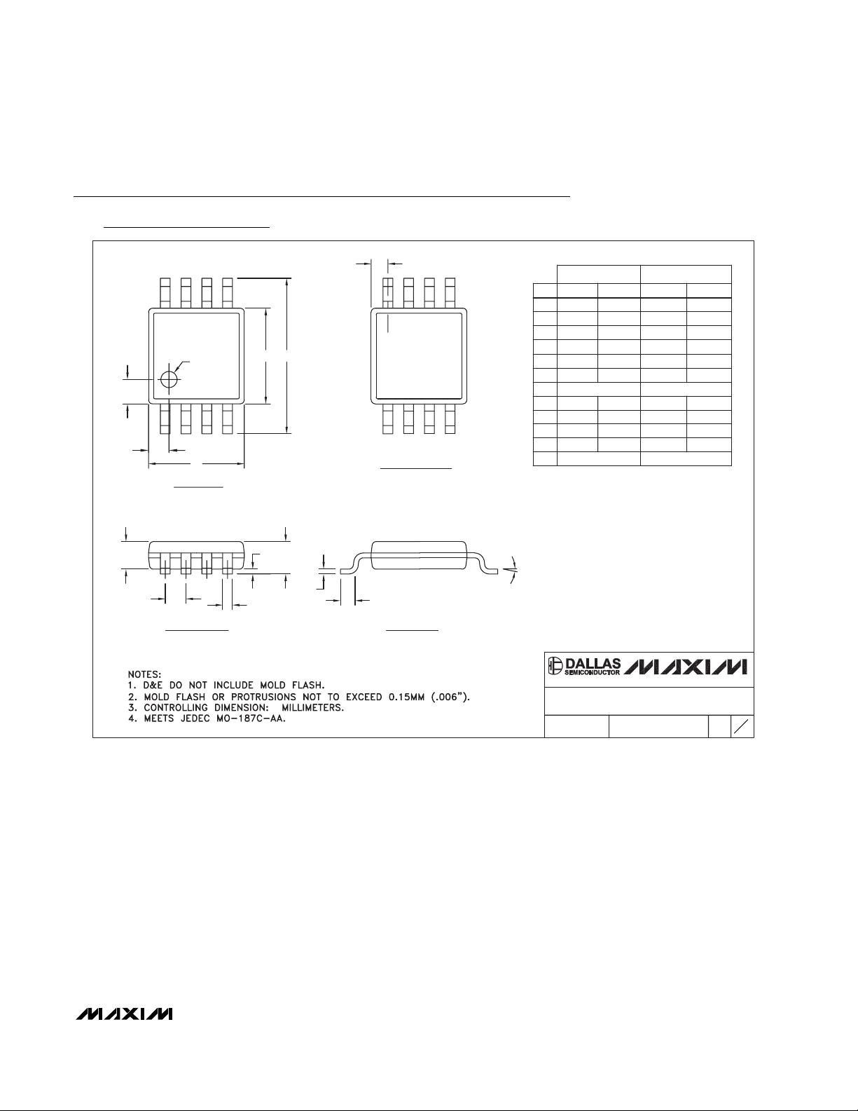
8LUMAXD.EPS
PACKAGE OUTLINE, 8L uMAX/uSOP
1
1
21-0036
J
REV.DOCUMENT CONTROL NO.APPROVAL
PROPRIETARY INFORMATION
TITLE:
MAX
0.043
0.006
0.014
0.120
0.120
0.198
0.026
0.007
0.037
0.0207 BSC
0.0256 BSC
A2
A1
c
e
b
A
L
FRONT VIEW
SIDE VIEW
E H
0.6±0.1
0.6±0.1
Ø0.50±0.1
1
TOP VIEW
D
8
A2
0.030
BOTTOM VIEW
1
6°
S
b
L
H
E
D
e
c
0°
0.010
0.116
0.116
0.188
0.016
0.005
8
4X S
INCHES
-
A1
A
MIN
0.002
0.950.75
0.5250 BSC
0.25 0.36
2.95 3.05
2.95 3.05
4.78
0.41
0.65 BSC
5.03
0.66
6°0°
0.13 0.18
MAX
MIN
MILLIMETERS
- 1.10
0.05 0.15
α
α
DIM
Package Information
(The package drawing(s) in this data sheet may not reflect the most current specifications. For the latest package outline information,
go to www.maxim-ic.com/packages
.)
MAX1236–MAX1239
Page 22

2.7V to 3.6V and 4.5V to 5.5V, Low-Power,
4-/12-Channel, 2-Wire Serial, 12-Bit ADCs
Maxim cannot assume responsibility for use of any circuitry other than circuitry entirely embodied in a Maxim product. No circuit patent licenses are
implied. Maxim reserves the right to change the circuitry and specifications without notice at any time.
22 ____________________Maxim Integrated Products, 120 San Gabriel Drive, Sunnyvale, CA 94086 408-737-7600
© 2006 Maxim Integrated Products is a registered trademark of Maxim Integrated Products, Inc.
QSOP.EPS
F
1
1
21-0055
PACKAGE OUTLINE, QSOP .150", .025" LEAD PITCH
Package Information (continued)
(The package drawing(s) in this data sheet may not reflect the most current specifications. For the latest package outline information,
go to www.maxim-ic.com/packages
.)
MAX1236–MAX1239
Revision History
Pages changed at Rev 4: 1, 15, 22
 Loading...