

Page 1
General Description
The MAX1233/MAX1234 are complete PDA controllers in
5mm × 5mm, 28-pin QFN and TQFN packages. They feature a 12-bit analog-to-digital converter (ADC), low onresistance switches for driving resistive touch screens, an
internal +1.0V/+2.5V or external reference, ±2°C accurate, on-chip temperature sensor, direct +6V battery monitor, keypad controller, 8-bit digital-to-analog converter
(DAC), and a synchronous serial interface. Each of the
keypad controllers’ eight row and column inputs can be
reconfigured as general-purpose parallel I/O pins (GPIO).
All analog inputs are fully ESD protected, eliminating the
need for external TransZorb™ devices.
The MAX1233/MAX1234 offer programmable resolution
and sampling rates. Interrupts from the devices alert the
host processor when data is ready, when the screen is
touched, or a key press is detected. Softwareconfigurable scan control and internal timers give the user
flexibility without burdening the host processor. These
devices consume only 260µA at the maximum sampling
rate of 50ksps. Supply current falls to below 50µA for
sampling rates of 10ksps. The MAX1233/MAX1234 are
guaranteed over the -40°C to +85°C temperature range.
Applications
Personal Digital Assistants
Pagers
Touch-Screen Monitors
Cellular Phones
MP3 Players
Portable Instruments
Point-of-Sale Terminals
Features
♦ ESD-Protected Analog Inputs
±15kV IEC 1000-4-2 Air-Gap Discharge
±8kV IEC 1000-4-2 Contact Discharge
♦ Single-Supply Operation
+2.7V to +3.6V (MAX1233)
+4.75V to +5.25V (MAX1234)
♦ 4-Wire Touch-Screen Interface
♦ Internal +1.0V/+2.5V Reference or External
Reference (+1.0V to AVDD)
♦ SPI™/QSPI™/MICROWIRE™-Compatible 10MHz
Serial Interface
♦ 12-Bit, 50ksps ADC Measures
Resistive Touch-Screen Position and Pressure
Two Auxiliary Analog Inputs
Two Battery Voltages (0.5V to 6V)
On-Chip Temperature
♦ 8-Bit DAC for LCD Bias Control
♦ 4 × 4 Keypad Programmable Controller Offers Up
to Eight GPIO Pins
♦ Automatic Detection of Screen Touch, Key Press,
and End of Conversion
♦ Programmable 8-, 10-, 12-Bit Resolution
♦ Programmable Conversion Rates
♦ AutoShutdown
™
Between Conversions
♦ Low Power
260µA at 50ksps
50µA at 10ksps
6µA at 1ksps
0.3µA Shutdown Current
♦ 28-Pin 5mm × 5mm QFN and TQFN Packages
MAX1233/MAX1234
±15kV ESD-Protected Touch-Screen
Controllers Include DAC and Keypad Controller
________________________________________________________________
Maxim Integrated Products
1
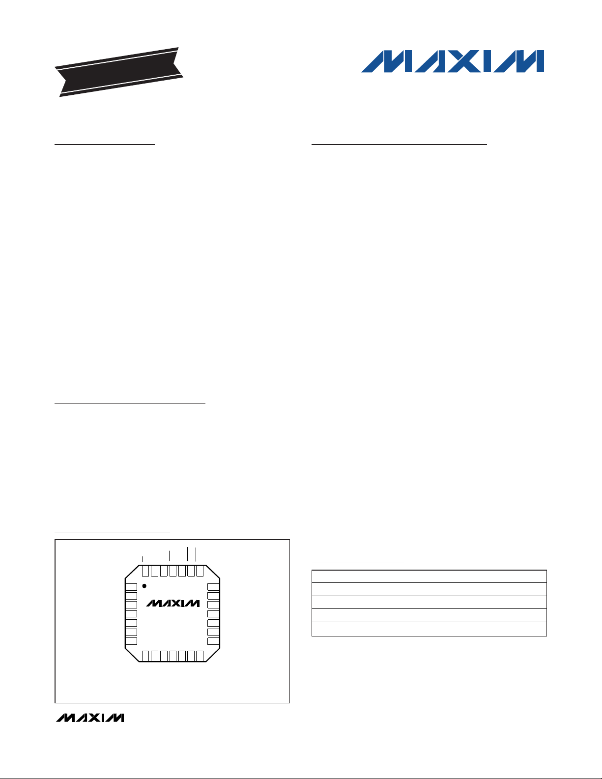
Pin Configuration
Ordering Information
19-2512; Rev 4; 3/08
For pricing, delivery, and ordering information, please contact Maxim Direct at 1-888-629-4642,
or visit Maxim’s website at www.maxim-ic.com.
EVALUATION KIT
AVAILABLE
TransZorb is a trademark of General Semiconductor Industries, Inc.
SPI and QSPI are trademarks of Motorola, Inc.
MICROWIRE is a trademark of National Semiconductor Corp.
AutoShutdown is a trademark of Maxim Integrated Products, Inc.
TOP VIEW
1
DV
DD
2
AV
DD
3
*X+
4
*Y+
5
*X-
6
*Y-
7
GND
*PIN INCLUDES 8kV/15kV ESD PROTECTION.
DIN
DOUT
PENIRQ
BUSY
SCLK
CS
28272625242322
MAX1233
MAX1234
8
9
1011121314
*BAT2
*AUX1
*AUX2
QFN/TQFN
REF
DACOUT
*BAT1
KEYIRQ
R4
21
C4
20
C3
19
C2
18
C1
17
R1
16
R2
15
R3
PART TEMP RANGE PIN-PACKAGE
MAX1233EGI -40°C to +85°C 28 QFN (5mm x 5mm)
MAX1233ETI -40°C to +85°C 28 TQFN (5mm x 5mm)
MAX1234EGI -40°C to +85°C 28 QFN (5mm x 5mm)
MAX1234ETI -40°C to +85°C 28 TQFN (5mm x 5mm)
Page 2
MAX1233/MAX1234
±15kV ESD-Protected Touch-Screen
Controllers Include DAC and Keypad Controller
2 _______________________________________________________________________________________
ABSOLUTE MAXIMUM RATINGS
ELECTRICAL CHARACTERISTICS
(DVDD= AVDD= +2.7V to +3.6V (MAX1233), DVDD= AVDD= +4.75V to +5.25V (MAX1234), external reference V
REF
= 2.5V
(MAX1233), V
REF
= 4.096V (MAX1234); f
SCLK
= 10MHz, f
SAMPLE
= 50ksps, 12-bit mode, 0.1µF capacitor at REF, TA= -40°C to
+85°C, unless otherwise noted. Typical values are at T
A
= +25°C.)
Stresses beyond those listed under “Absolute Maximum Ratings” may cause permanent damage to the device. These are stress ratings only, and functional
operation of the device at these or any other conditions beyond those indicated in the operational sections of the specifications is not implied. Exposure to
absolute maximum rating conditions for extended periods may affect device reliability.
AVDDto GND............................................................-0.3V to +6V
DV
DD
to AVDD.......................................................-0.3V to +0.3V
Digital Inputs/Outputs to GND .................-0.3V to (DV
DD
+ 0.3V)
X+, Y+, X-, Y-, AUX1, AUX2,
and REF to GND ..................................-0.3V to (AV
DD
+ 0.3V)
BAT1, BAT2 to GND .................................................-0.3V to +6V
Maximum ESD per IEC 1000-4-2 (per MIL STD-883 HBM)
X+, X-, Y+, Y-, AUX1, AUX2, BAT1, BAT2......................±15kV
All Other Pins.....................................................................±2.5kV
Maximum Current into Any Pin............................................50mA
Continuous Power Dissipation (T
A
= +70°C)
28-Pin QFN (derate 28.5mW/°C above +70°C) .................2W
28-Pin TQFN (derate 28.5mW/°C above +70°C) ...............2W
Operating Temperature Range ...........................-40°C to +85°C
Storage Temperature Range .............................-60°C to +150°C
Lead Temperature (soldering, 10s) .................................+300°C
DC ACCURACY (Note 1)
Resolution Software-programmable 8/10/12 bit 12 Bits
No Missing Codes 11 Bits
Relative Accuracy (Note 2) INL
Differential Nonlinearity DNL
Offset Error
Total Unadjusted Error TUE
Offset Temperature Coefficient ±0.4 ppm/°C
Gain Temperature Coefficient ±0.4 ppm/°C
Channel-to-Channel Offset ±0.1 LSB
Channel-to-Channel Gain
Matching
Noise Including internal V
Power-Supply Rejection PSR
DYNAMIC SPECIFICATIONS (1kHz SINE WAVE, VIN = 2.5V
= 10MHz)
f
SCLK
Signal-to-Noise Plus Distortion SINAD 69 dB
PARAMETER SYMBOL CONDITIONS MIN TYP MAX UNITS
ANALOG-TO-DIGITAL CONVERTER
12-bit mode ±0.8 ±2
10-bit and 8-bit modes ±0.5
12-bit mode ±0.8 ±2
10-bit and 8-bit modes ±0.5
12-bit mode ±0.5 ±4
10-bit and 8-bit modes ±0.5
12-bit mode ±0.5 ±4
10-bit mode ±0.5Gain Error (Note 3)
8-bit mode ±0.5
12-bit mode ±2
10-bit and 8-bit modes ±1
Full-scale
input
REF
MAX1233
AV
= DVDD = +2.7V to +3.6V
DD
MAX1234
AV
= DVDD = +5V ±5%
DD
FOR MAX1233, VIN = 4.096V
P-P
±0.1 LSB
50 µV
±0.4
±0.3
FOR MAX1234, 50ksps,
P-P
LSB
LSB
LSB
LSB
LSB
RMS
mV
Page 3

MAX1233/MAX1234
±15kV ESD-Protected Touch-Screen
Controllers Include DAC and Keypad Controller
_______________________________________________________________________________________ 3
ELECTRICAL CHARACTERISTICS (continued)
(DVDD= AVDD= +2.7V to +3.6V (MAX1233), DVDD= AVDD= +4.75V to +5.25V (MAX1234), external reference V
REF
= 2.5V
(MAX1233), V
REF
= 4.096V (MAX1234); f
SCLK
= 10MHz, f
SAMPLE
= 50ksps, 12-bit mode, 0.1µF capacitor at REF, TA= -40°C to
+85°C, unless otherwise noted. Typical values are at T
A
= +25°C.)
Total Harmonic Distortion THD -84 dB
Spurious-Free Dynamic Range SFDR 84 dB
Full-Power Bandwidth -3dB point 0.5 MHz
Full-Linear Bandwidth SINAD > 67dB 50 kHz
CONVERSION RATE
Internal Oscillator Frequency 8 11.5 MHz
Aperture Delay 30 ns
Aperture Jitter <50 ps
Maximum Serial Clock Frequency f
Duty Cycle 30 70 %
AUXILIARY ANALOG INPUTS (AUX1, AUX2)
Input Voltage Range 0V
Input Leakage Current
Input Capacitance 34 pF
BATTERY MONITOR INPUTS (BAT1, BAT2)
Input Voltage Range 0.5 6.0 V
Input Impedance
Accuracy Internal reference -3 +3 %
TEMPERATURE MEASUREMENT
Temperature Range -40 +85 °C
Resolution
Accuracy
INTERNAL ADC REFERENCE
Reference Output Voltage V
Output Tempco TCV
Reference Output Impedance Normal operation 250 Ω
Reference Short-Circuit Current 18 mA
EXTERNAL ADC REFERENCE (INTERNAL REFERENCE DISABLED, REFERENCE APPLIED TO REF)
Reference Input Voltage Range (Note 6) 1.0 V
Input Impedance CS = GND or V
Input Current
PARAMETER SYMBOL CONDITIONS MIN TYP MAX UNITS
SCLK
REF
REF
Channel not selected or conversion
stopped
Sampling battery 10 kΩ
Battery monitor OFF 1 GΩ
Differential method (Note 4) 1.6
Single measurement method (Note 5) 0.3
Differential method (Note 4) ±3
Single measurement method (Note 5) ±2
2.5V mode, TA = +25°C 2.470 2.500 2.530
1.0V mode, TA = +25°C 0.980 1.000 1.020
V
V
Shutdown/between conversions ±0.1
= +2.5V at 50ksps (MAX1233) 5 10
REF
= +4.096V at 50ksps (MAX1234) 8 15
REF
10 MHz
REF
±0.1 ±1µA
60 ppm/°C
DD
1GΩ
DD
°C
°C
µA
V
V
V
Page 4
MAX1233/MAX1234
±15kV ESD-Protected Touch-Screen
Controllers Include DAC and Keypad Controller
4 _______________________________________________________________________________________
ELECTRICAL CHARACTERISTICS (continued)
(DVDD= AVDD= +2.7V to +3.6V (MAX1233), DVDD= AVDD= +4.75V to +5.25V (MAX1234), external reference V
REF
= 2.5V
(MAX1233), V
REF
= 4.096V (MAX1234); f
SCLK
= 10MHz, f
SAMPLE
= 50ksps, 12-bit mode, 0.1µF capacitor at REF, TA= -40°C to
+85°C, unless otherwise noted. Typical values are at T
A
= +25°C.)
DC ACCURACY
Resolution 8Bits
Integral Linearity Error INL (Note 7) ±1.0 LSB
Differential Linearity Error DNL No missing codes ±1.0 LSB
Offset Error V
Offset Error Temperature
Coefficient
Full-Scale Error Code = 255, no load 5 %
Full-Scale Error Temperature
Coefficient
DYNAMIC PERFORMANCE
Voltage Output Slew Rate Positive and negative 0.4 V/µs
Output Settling Time 0.5LSB; 50kΩ and 50pF load (Note 9) 20 µs
Glitch Impulse Code 127 to 128 40 nV/s
Wake-Up Time From shutdown 50 µs
DAC OUTPUT
Internal DAC Reference V
Output Load Regulation
Output Resistance Power-down mode 1.0 MΩ
On-Resistance
Touch-Detection Internal Pullup
Resistance
Pullup Resistance C4, C3, C2, C1 (Note 11) 0.5 kΩ
Pulldown Resistance R4, R3, R2, R1 (Note 11) 16 kΩ
DIGITAL INPUTS (SCLK, CS, DIN, R_, C_)
Input Voltage Low V
Input Voltage High V
Input Leakage Current I
PARAMETER SYMBOL CONDITIONS MIN TYP MAX UNITS
REFDAC
DIGITAL-TO-ANALOG CONVERTER
OS
(Note 8) ±1 ±25 mV
Code = 255, no load ±10 ppm/°C
(Note 10)
Code = 255; 0 to 100µA 0.5
Code = 0; 0 to 100µA 0.5
TOUCH-SCREEN CONTROLLER
Y+, X+ 7
Y-, X- 9
X+ to AV
IL
IH
L
DD
KEYPAD CONTROLLER
DIGITAL INTERFACE
0.85
AV
0.7
DV
1 ppm/°C
✕
DD
✕
DD
✕
0.9
AV
DD
1MΩ
±0.1 ±1µA
0.95
AV
0.3
DV
✕
DD
✕
DD
V
LSB
Ω
V
V
Page 5
MAX1233/MAX1234
±15kV ESD-Protected Touch-Screen
Controllers Include DAC and Keypad Controller
_______________________________________________________________________________________ 5
ELECTRICAL CHARACTERISTICS (continued)
(DVDD= AVDD= +2.7V to +3.6V (MAX1233), DVDD= AVDD= +4.75V to +5.25V (MAX1234), external reference V
REF
= 2.5V
(MAX1233), V
REF
= 4.096V (MAX1234); f
SCLK
= 10MHz, f
SAMPLE
= 50ksps, 12-bit mode, 0.1µF capacitor at REF, TA= -40°C to
+85°C, unless otherwise noted. Typical values are at T
A
= +25°C.)
Note 1: Tested at DVDD= AVDD= +2.7V (MAX1233), DVDD= AVDD= +5V (MAX1234).
Note 2: Relative accuracy is the deviation of the analog value at any code from its theoretical value after the offset and gain errors
have been removed.
Note 3: Offset nulled.
Note 4: Difference between TEMP1 and TEMP2; temperature in °K = (V
TEMP2
- V
TEMP1
) × 2680°K/V. No calibration is necessary.
Note 5: Temperature coefficient is -2.1mV/°C. Determine absolute temperature by extrapolating from a calibrated value.
Note 6: ADC performance is limited by the conversion noise floor, typically 300µV
P-P
. An external reference below 2.5V can
compromise the ADC performance.
Note 7: Guaranteed from code 5 to 255.
Input Capacitance C
DIGITAL OUTPUT (DOUT)
Output Voltage Low V
Output Voltage High V
DIGITAL OUTPUT (BUSY, PENIRQ, KEYIRQ, R_, C_)
Output Voltage Low V
Output Voltage High V
Supply Voltage (Note 12)
Analog and Digital Supply
Current
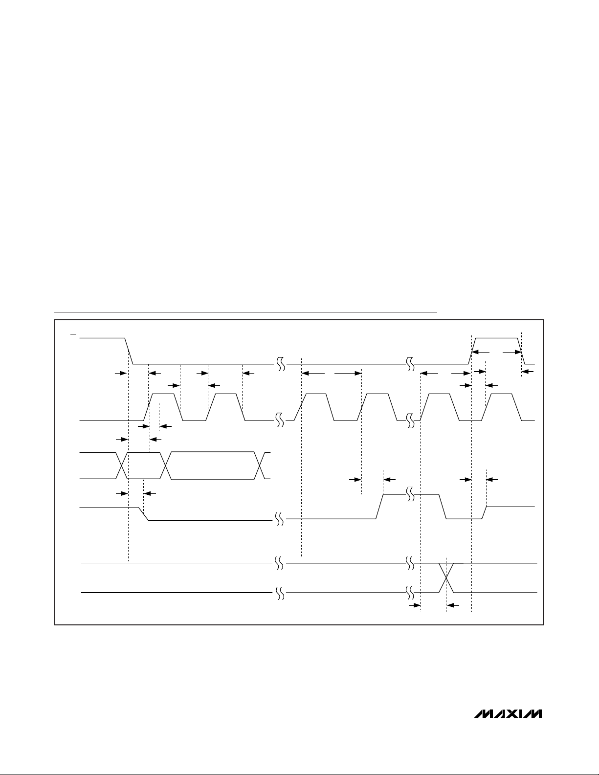
TIMING CHARACTERISTICS
SCLK Clock Period t
SCLK Pulse Width High t
SCLK Pulse Width Low t
DIN to SCLK Rise Setup t
SCLK Rise to DIN Hold t
SCLK Fall to DOUT Valid t
CS Fall to DOUT Enabled t
CS Rise to DOUT Disabled t
CS Fall to SCLK Rise t
CS Fall to SCLK Ignored t
SCLK Rise to R_/C_ Data Valid t
CS Pulse Width High t
PARAMETER SYMBOL CONDITIONS MIN TYP MAX UNITS
IN
OL
OH
OL
OH
15 pF
I
= 2mA 0.4
SINK
I
= 4mA 0.8
SINK
DV
-
DV
DD
0.5
DD
0.5
-
I
I
I
= 1.5mA
SOURCE
= 0.2mA 0.4 V
SINK
= 0.2mA
SOURCE
POWER REQUIREMENTS
AV
DV
DD
MAX1233 2.7 3 3.6
/
DD MAX1234 4.75 5 5.25
Idle; all blocks shut down 0.5 5
I
AVDD
I
DVDD
Only ADC on; f
+
Only DAC on; no load 150 230
= 20ksps 150 500
SAMPLE
Only internal reference on 670 900
CP
CH
CL
DS
DH
DOV
DV
DOD
CSS
CSH
GPO
CSW
C
= 50pF 40 ns
LOAD
C
= 50pF 45 ns
LOAD
C
= 50pF 40 ns
LOAD
C
= 50pF (Note 13) 230 ns
LOAD
100 ns
40 ns
40 ns
40 ns
0ns
40 ns
0ns
40 ns
V
V
V
V
µA
Page 6
MAX1233/MAX1234
±15kV ESD-Protected Touch-Screen
Controllers Include DAC and Keypad Controller
6 _______________________________________________________________________________________
ELECTRICAL CHARACTERISTICS (continued)
(DVDD= AVDD= +2.7V to +3.6V (MAX1233), DVDD= AVDD= +4.75V to +5.25V (MAX1234), external reference V
REF
= 2.5V
(MAX1233), V
REF
= 4.096V (MAX1234); f
SCLK
= 10MHz, f
SAMPLE
= 50ksps, 12-bit mode, 0.1µF capacitor at REF, TA= -40°C to
+85°C, unless otherwise noted. Typical values are at T
A
= +25°C.)
Note 8: The offset value extrapolated from the range over which the INL is guaranteed.
Note 9: Output settling time is measured by stepping from code 5 to 255, and from code 255 to 5.
Note 10: Actual output voltage at full scale is 255/256 × V
REFDAC
.
Note 11: Resistance is open when configured as GPIO or in shutdown.
Note 12: AV
DD
and DVDDshould not differ by more than 300mV.
Note 13: When configured as GPIO.
SCLK
DIN
DOUT
NOTE: TIMING NOT TO SCALE.
R_/C_
CS
t
CL
t
DH
t
DV
t
DS
t
CH
t
CSS
t
CP
t
CSH
t
CSW
t
CSH
t
CSS
t
DOD
t
DOV
t
GPO
Timing Diagram
Page 7
MAX1233/MAX1234
±15kV ESD-Protected Touch-Screen
Controllers Include DAC and Keypad Controller
_______________________________________________________________________________________ 7
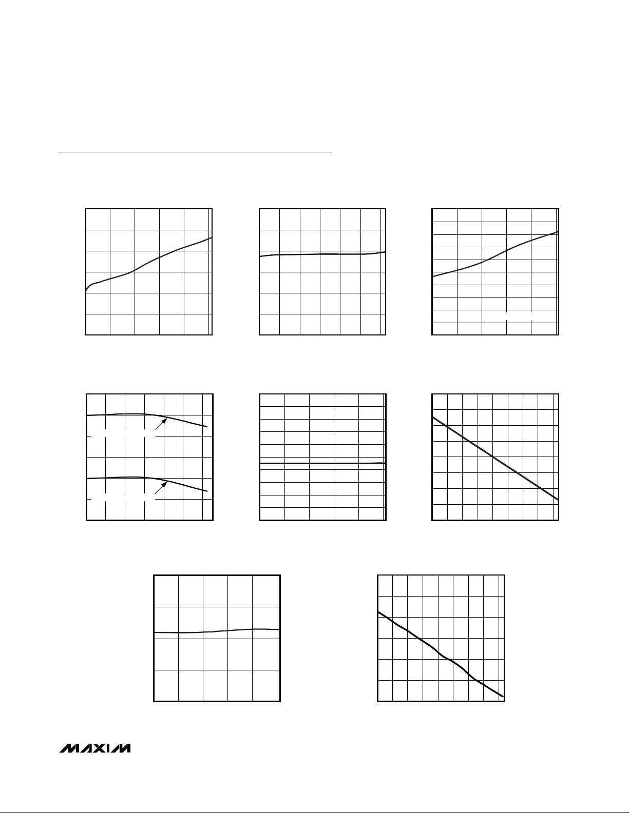
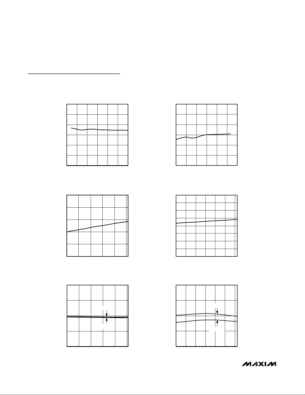
Typical Operating Characteristics
(AV
DD
= DVDD= 3V (MAX1233) or 5V (MAX1234), external V
REF
= +2.5V (MAX1233), external V
REF
= +4.096V (MAX1234), f
SCLK
=
10MHz (50% duty cycle), f
SAMPLE
= 20ksps, C
LOAD
= 50pF, 0.1µF capacitor at REF, TA= +25°C, unless otherwise noted.)
SHUTDOWN CURRENT
vs. ANALOG SUPPLY VOLTAGE
300
250
200
150
100
SHUTDOWN CURRENT (nA)
50
0
2.7
AVDD (V)
MAX1233/34 toc01
5.24.74.23.73.2
INTERNAL OSCILLATOR FREQUENCY
vs. TEMPERATURE
9.8
9.6
MAX1234, AVDD = +5.0V
9.4
9.2
9.0
MAX1233, AVDD = +3.0V
8.8
INTERNAL OSCILLATOR FREQUENCY (MHz)
8.6
-40
TEMPERATURE (°C)
MAX1233/34 toc04
806040200-20
TEMP2 DIODE VOLTAGE
vs. ANALOG SUPPLY VOLTAGE
0.80
SHUTDOWN CURRENT
vs. TEMPERATURE
300
250
200
150
100
SHUTDOWN CURRENT (nA)
50
0
-40
TEMPERATURE (°C)
806040200-20
10.0
MAX1233/34 toc02
INTERNAL OSCILLATOR FREQUENCY (MHz)
TEMP1 DIODE VOLTAGE
vs. ANALOG SUPPLY VOLTAGE
0.70
0.68
0.66
0.64
0.62
0.60
0.58
0.56
TEMP1 DIODE VOLTAGE (V)
0.54
0.52
0.50
2.7
5.24.74.23.73.2
AVDD (V)
0.80
0.75
MAX1233/34 toc05
0.70
0.65
0.60
0.55
TEMP1 DIODE VOLTAGE (V)
0.50
0.45
0.40
TEMP2 DIODE VOLTAGE
vs. TEMPERATURE
0.90
INTERNAL OSCILLATOR FREQUENCY
vs. ANALOG SUPPLY VOLTAGE
9.8
9.6
9.4
9.2
9.0
8.8
8.6
8.4
8.2
8.0
2.7
TEMP1 DIODE VOLTAGE
vs. TEMPERATURE
-40
TEMPERATURE (°C)
MAX1233/MAX1234
AVDD (V)
8065-25 -10 5 3520 50
MAX1233/34 toc03
5.24.74.23.73.2
MAX1233/34 toc06
0.75
0.70
TEMP2 DIODE VOLTAGE (V)
0.65
0.60
2.7
AVDD (V)
5.24.74.23.73.2
MAX1233/34 toc07
0.85
0.80
0.75
0.70
TEMP2 DIODE VOLTAGE (V)
0.65
0.60
-40
TEMPERATURE (°C)
MAX1233/34 toc08
80655035205-10-25
Page 8
MAX1233/MAX1234
±15kV ESD-Protected Touch-Screen
Controllers Include DAC and Keypad Controller
8 _______________________________________________________________________________________
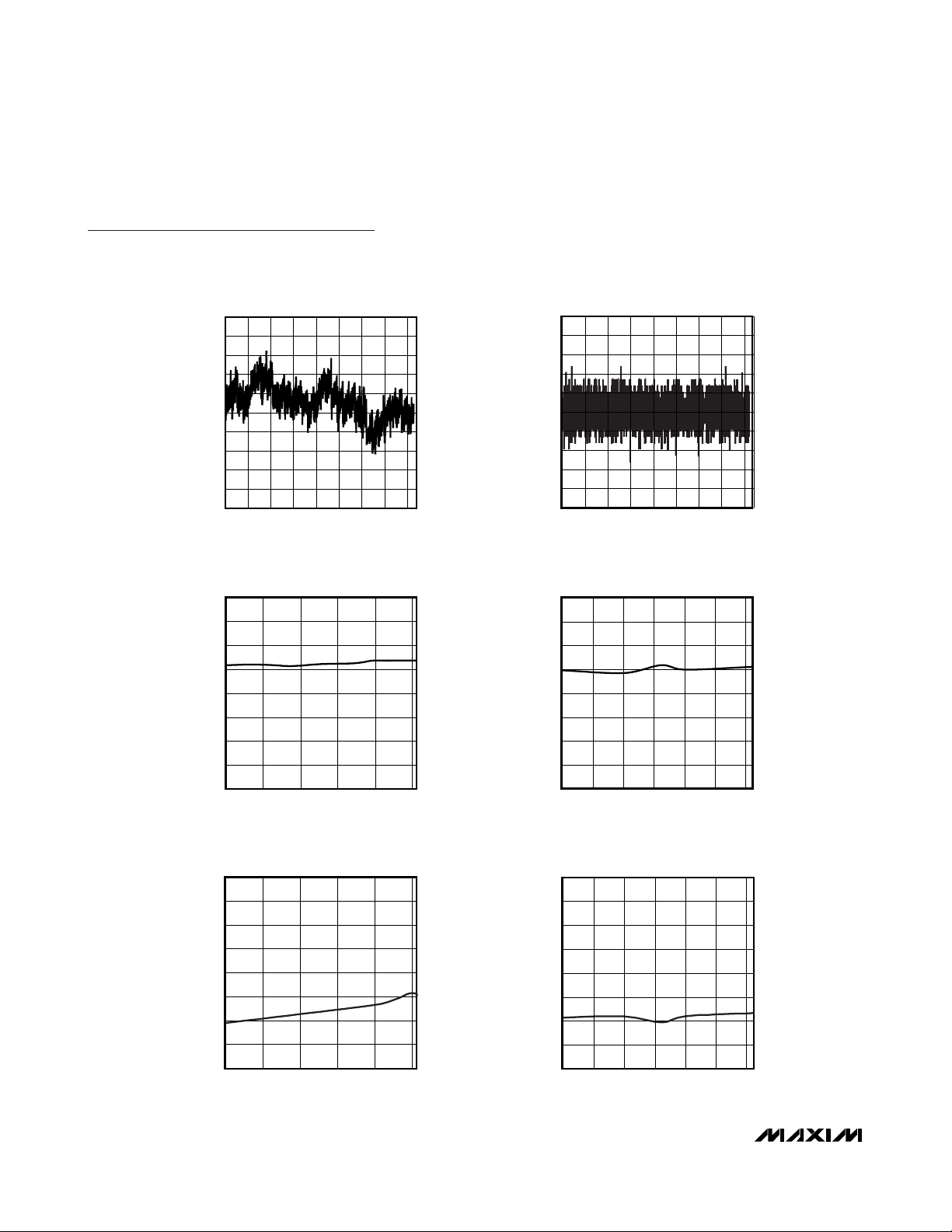
Typical Operating Characteristics (continued)
(AV
DD
= DVDD= 3V (MAX1233) or 5V (MAX1234), external V
REF
= +2.5V (MAX1233), external V
REF
= +4.096V (MAX1234), f
SCLK
=
10MHz (50% duty cycle), f
SAMPLE
= 20ksps, C
LOAD
= 50pF, 0.1µF capacitor at REF, TA= +25°C, unless otherwise noted.)
ADC DIFFERENTIAL NONLINEARITY
vs. OUTPUT CODE
MAX1233/34 toc10
OUTPUT CODE
DNL (LSB)
400035002500 30001000 1500 2000500
-0.8
-0.6
-0.4
-0.2
0
0.2
0.4
0.6
0.8
1.0
-1.0
0
ADC OFFSET ERROR
vs. ANALOG SUPPLY VOLTAGE
MAX1233/34 toc11
AVDD (V)
OFFSET ERROR (LSB)
5.24.73.2 3.7 4.2
-1.5
-1.0
-0.5
0
0.5
1.0
1.5
2.0
-2.0
2.7
ADC OFFSET ERROR vs. TEMPERATURE
MAX1233/34 toc12
TEMPERATURE (°C)
OFFSET ERROR (LSB)
8060-20 0 20 40
-1.5
-1.0
-0.5
0
0.5
1.0
1.5
2.0
-2.0
-40
ADC GAIN ERROR
vs. ANALOG SUPPLY VOLTAGE
MAX1233/34 toc13
AVDD (V)
GAIN ERROR (LSB)
5.24.73.2 3.7 4.2
-1.5
-1.0
-0.5
0
0.5
1.0
1.5
2.0
-2.0
2.7
ADC GAIN ERROR
vs. TEMPERATURE
MAX1233/34 toc14
TEMPERATURE (°C)
GAIN ERROR (LSB)
-1.5
-1.0
-0.5
0
0.5
1.0
1.5
2.0
-2.0
8060-20 0 20 40-40
ADC INTEGRAL NONLINEARITY
vs. OUTPUT CODE
MAX1233/34 toc09
OUTPUT CODE
INL (LSB)
400035002500 30001000 1500 2000500
-0.8
-0.6
-0.4
-0.2
0
0.2
0.4
0.6
0.8
1.0
-1.0
0
Page 9
MAX1233/MAX1234
-0.050
-0.075
-0.100
-0.025
0
0.025
0.050
0.075
0 100 200 300
DAC INTEGRAL NONLINEARITY vs. CODE
MAX1233/34 toc19
CODE
INL (LSB)
50
150
250
DAC DIFFERENTIAL NONLINEARITY
vs. OUTPUT CODE
MAX1233/34 toc20
OUTPUT CODE
DNL (LSB)
25020015010050
-0.075
-0.500
-0.025
0
0.025
0.050
0.075
-0.100
0 300
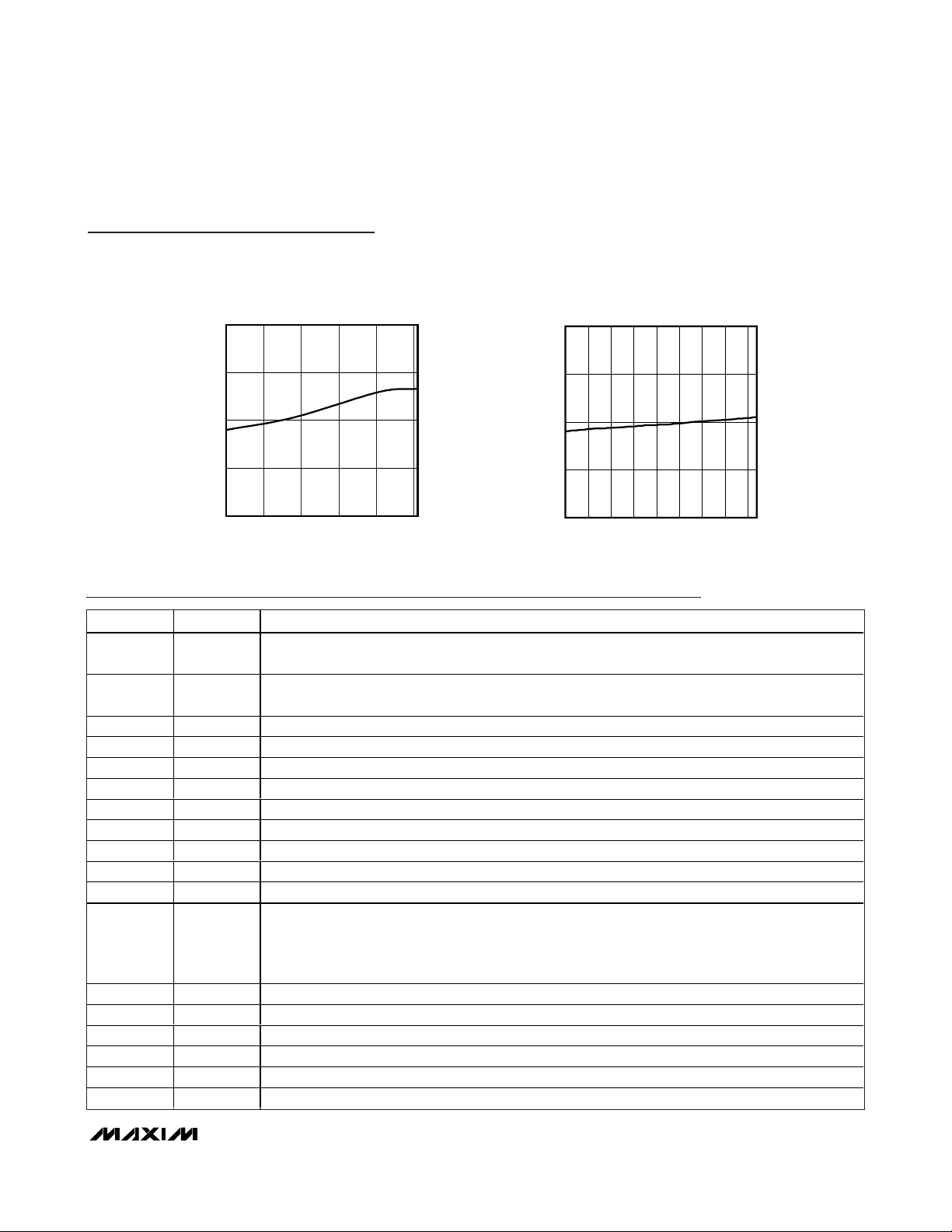
Typical Operating Characteristics (continued)
(AV
DD
= DVDD= 3V (MAX1233) or 5V (MAX1234), external V
REF
= +2.5V (MAX1233), external V
REF
= +4.096V (MAX1234), f
SCLK
=
10MHz (50% duty cycle), f
SAMPLE
= 20ksps, C
LOAD
= 50pF, 0.1µF capacitor at REF, TA= +25°C, unless otherwise noted.)
±15kV ESD-Protected Touch-Screen
Controllers Include DAC and Keypad Controller
_______________________________________________________________________________________ 9
ADC EXTERNAL REFERENCE INPUT
CURRENT vs. SAMPLING RATE
8
MAX1233
= +2.5V
V
REF
6
1000
MAX1233/34 toc15
100
ADC SUPPLY CURRENT
vs. SAMPLING RATE
MAX1233/34 toc16
4
REFERENCE CURRENT (μA)
2
0
100 100k
f
SAMPLE
10k1k
(Hz)
ADC SUPPLY CURRENT
vs. SUPPLY VOLTAGE
250
200
150
100
SUPPLY CURRENT (μA)
50
0
AVDD (V)
EXTERNAL REF
= 20ksps
f
SAMPLE
5.24.74.23.73.22.7
MAX1233/34 toc17
10
SUPPLY CURRENT (μA)
1
0.1
1 100k10 1k
ADC SUPPLY CURRENT
140
120
100
80
60
SUPPLY CURRENT (μA)
40
20
0
f
(Hz)
SAMPLE
vs. TEMPERATURE
TEMPERATURE (°C)
10k100
AVDD = +3V
MAX1233/34 toc18
8060-20 0 20 40-40
Page 10
MAX1233/MAX1234
±15kV ESD-Protected Touch-Screen
Controllers Include DAC and Keypad Controller
10 ______________________________________________________________________________________
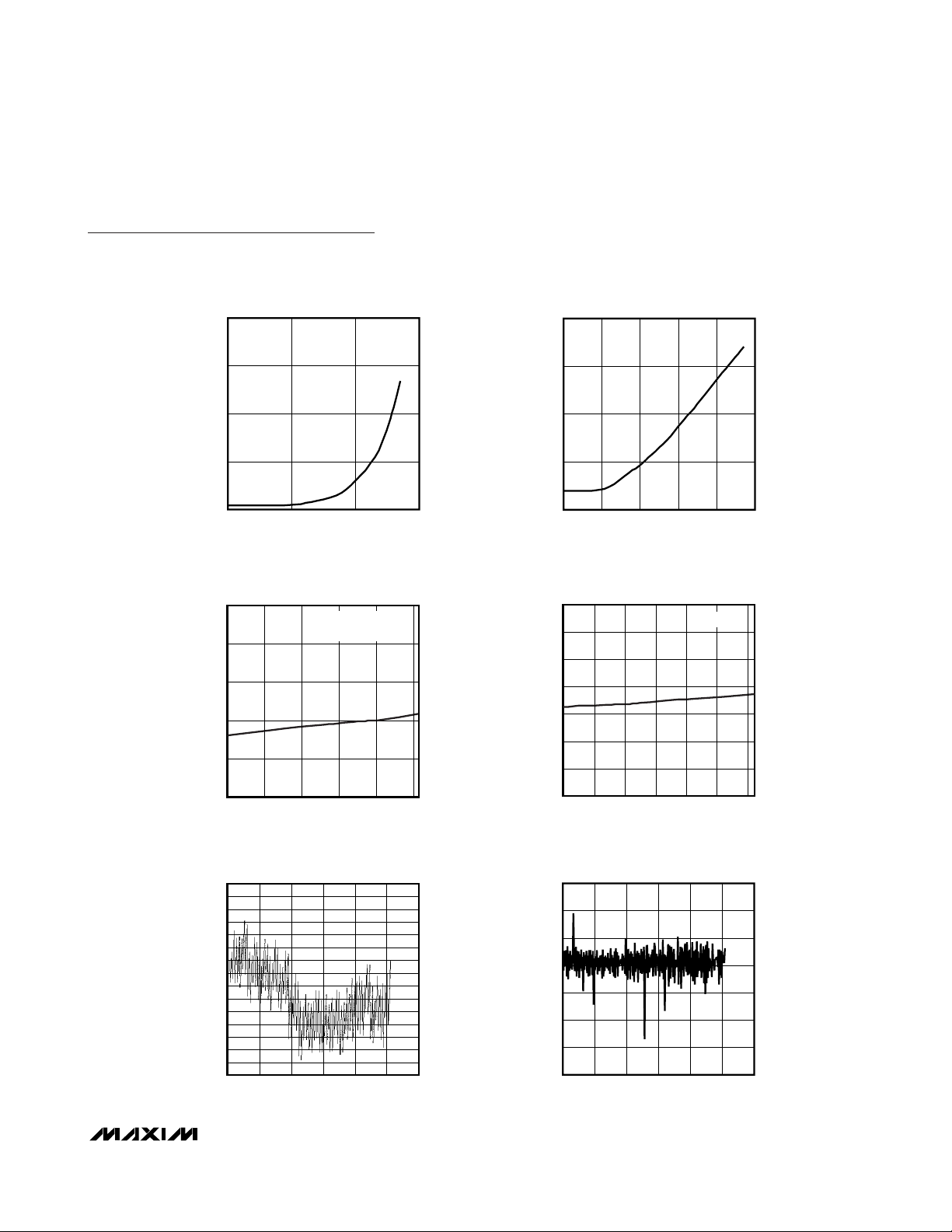
Typical Operating Characteristics (continued)
(AV
DD
= DVDD= 3V (MAX1233) or 5V (MAX1234), external V
REF
= +2.5V (MAX1233), external V
REF
= +4.096V (MAX1234), f
SCLK
=
10MHz (50% duty cycle), f
SAMPLE
= 20ksps, C
LOAD
= 50pF, 0.1µF capacitor at REF, TA= +25°C, unless otherwise noted.)
DAC FULL-SCALE ERROR
vs. ANALOG SUPPLY VOLTAGE
0.75
MAX1233/34 toc21
1.2
DAC FULL-SCALE ERROR
0.75
vs. TEMPERATURE
MAX1233/34 toc22
1.2
0.50
0.25
0
-0.25
FULL-SCALE ERROR (LSB)
-0.50
-0.75
2.5 4.03.0 3.5 4.5 5.0 5.5
AVDD (V)
DAC SUPPLY CURRENT
vs. ANALOG SUPPLY VOLTAGE
250
200
150
100
DAC SUPPLY CURRENT (μA)
50
0
AVDD (V)
5.24.74.23.73.22.7
0.8
0.4
0
-0.4
FULL-SCALE ERROR (%)
-0.8
-1.2
MAX1233/34 toc23
0.50
0.25
0
-0.25
FULL-SCALE ERROR (LSB)
-0.50
-0.75
-40 20-20 0 40 60 80
TEMPERATURE (°C)
DAC SUPPLY CURRENT
vs. TEMPERATURE
200
175
150
125
100
75
50
DAC SUPPLY CURRENT (μA)
25
0
-40
TEMPERATURE (°C)
0.8
0.4
0
-0.4
FULL-SCALE ERROR (%)
-0.8
-1.2
MAX1233/34 toc24
8060-20 0 20 40
ADC REFERENCE VOLTAGE
vs. TEMPERATURE
TEMPERATURE (°C)
MAX1233/34 toc26
V
= 1.0V
REF
V
= 2.5V
REF
(V)
V
REF
2.550
2.525
2.500
2.475
2.450
ADC REFERENCE VOLTAGE
vs. ANALOG SUPPLY VOLTAGE
V
AVDD (V)
MAX1233/34 toc25
= 1.0V
REF
V
= 2.5V
REF
(V)
REF
V
2.60
2.55
2.50
2.45
2.40
1.020
1.010
(V)
1.000
REF
V
0.990
0.980
5.24.74.23.73.22.7
1.250
1.125
(V)
1.000
REF
V
0.875
0.750
8060-20 0 20 40-40
Page 11
MAX1233/MAX1234
±15kV ESD-Protected Touch-Screen
Controllers Include DAC and Keypad Controller
______________________________________________________________________________________ 11
Typical Operating Characteristics (continued)
(AV
DD
= DVDD= 3V (MAX1233) or 5V (MAX1234), external V
REF
= +2.5V (MAX1233), external V
REF
= +4.096V (MAX1234), f
SCLK
=
10MHz (50% duty cycle), f
SAMPLE
= 20ksps, C
LOAD
= 50pF, 0.1µF capacitor at REF, TA= +25°C, unless otherwise noted.)
ADC REFERENCE SUPPLY CURRENT
vs. ANALOG SUPPLY VOLTAGE
MAX1233/34 toc27
AVDD (V)
SUPPLY CURRENT (μA)
4.74.23.73.2
600
650
700
750
550
2.7 5.2
REFERENCE SUPPLY CURRENT
vs. TEMPERATURE
MAX1233/34 toc28
TEMPERATURE (°C)
SUPPLY CURRENT (μA)
600
650
700
750
550
8065-25 -10 5 3520 50-40
PIN NAME FUNCTION
1DV
DD
Positive Digital Supply Voltage, +2.7V to +3.6V for MAX1233, +4.75V to +5.25V for MAX1234. Bypass
with a 0.1µF capacitor. Must be within 300mV of AV
DD
.
2AV
DD
Positive Analog Supply Voltage, +2.7V to +3.6V for MAX1233, +4.75V to +5.25V for MAX1234.
Bypass with a 0.1µF capacitor. Must be within 300mV of DV
DD
.
3* X+ X+ Position Input
4* Y+ Y+ Position Input
5* X- X- Position Input
6* Y- Y- Position Input
7 GND Analog and Digital Ground
8* BAT1 Battery Monitoring Input 1. Measures battery voltages up to 6V.
9* BAT2 Battery Monitoring Input 2. Measures battery voltages up to 6V.
10* AUX1 Auxiliary Analog Input 1 to ADC. Measures analog voltages from zero to V
REF
.
11* AUX2 Auxiliary Analog Input 2 to ADC. Measures analog voltages from zero to V
REF
.
12 REF
Voltage Reference Output/Input. Reference voltage for analog-to-digital conversion. In internal
reference mode, the reference buffer provides a 2.5V or 1.0V nominal output. In external reference
mode, apply a reference voltage between 1.0V and AV
DD
. Bypass REF to GND with a 0.1µF
capacitor in the external reference mode only.
13
DAC Voltage Output; 0.9 × AVDD Full Scale
14 R4 Keypad Row 4. Can be reconfigured as GPIO3.
15 R3 Keypad Row 3. Can be reconfigured as GPIO2.
16 R2 Keypad Row 2. Can be reconfigured as GPIO1.
17 R1 Keypad Row 1. Can be reconfigured as GPIO0.
18 C1 Keypad Column 1. Can be reconfigured as GPIO4.
Pin Description
DACOUT
Page 12

MAX1233/MAX1234
±15kV ESD-Protected Touch-Screen
Controllers Include DAC and Keypad Controller
12 ______________________________________________________________________________________
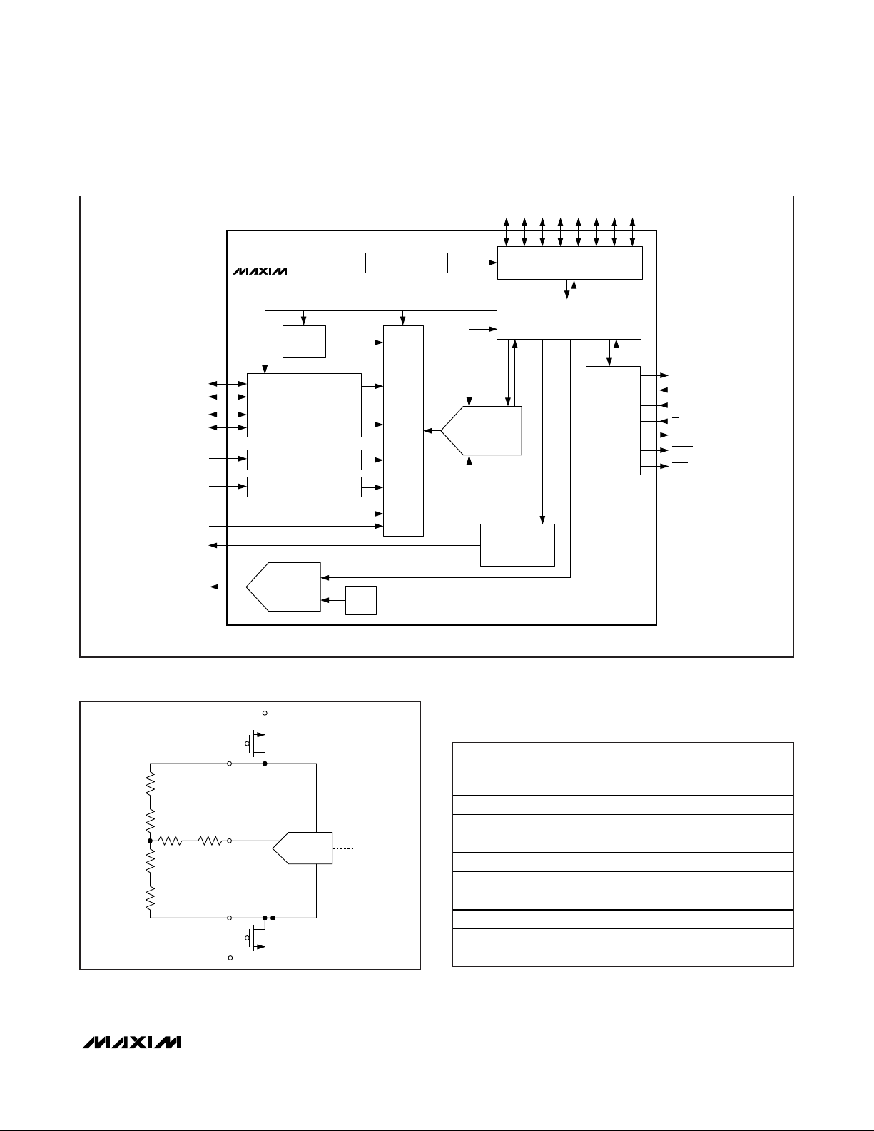
Detailed Description
The MAX1233/MAX1234 are 4-wire touch-screen controllers. Figure 1 shows the functional diagram of the
MAX1233/MAX1234. Each device includes a 12-bit sampling ADC, 8-bit voltage output DAC, keypad scanner
that can also be configured as a GPIO, internal clock,
reference, temperature sensor, two battery monitor
inputs, two auxiliary analog inputs, SPI/QSPI/
MICROWIRE-compatible serial interface, and low onresistance switches for driving touch screens.
The 16-bit register inside the MAX1233/MAX1234
allows for easy control and stores results that can be
read at any time. The BUSY output indicates that a
functional operation is in progress. The PENIRQ and
KEYIRQ outputs, respectively, indicate that a screen
touch or a key press has occurred.
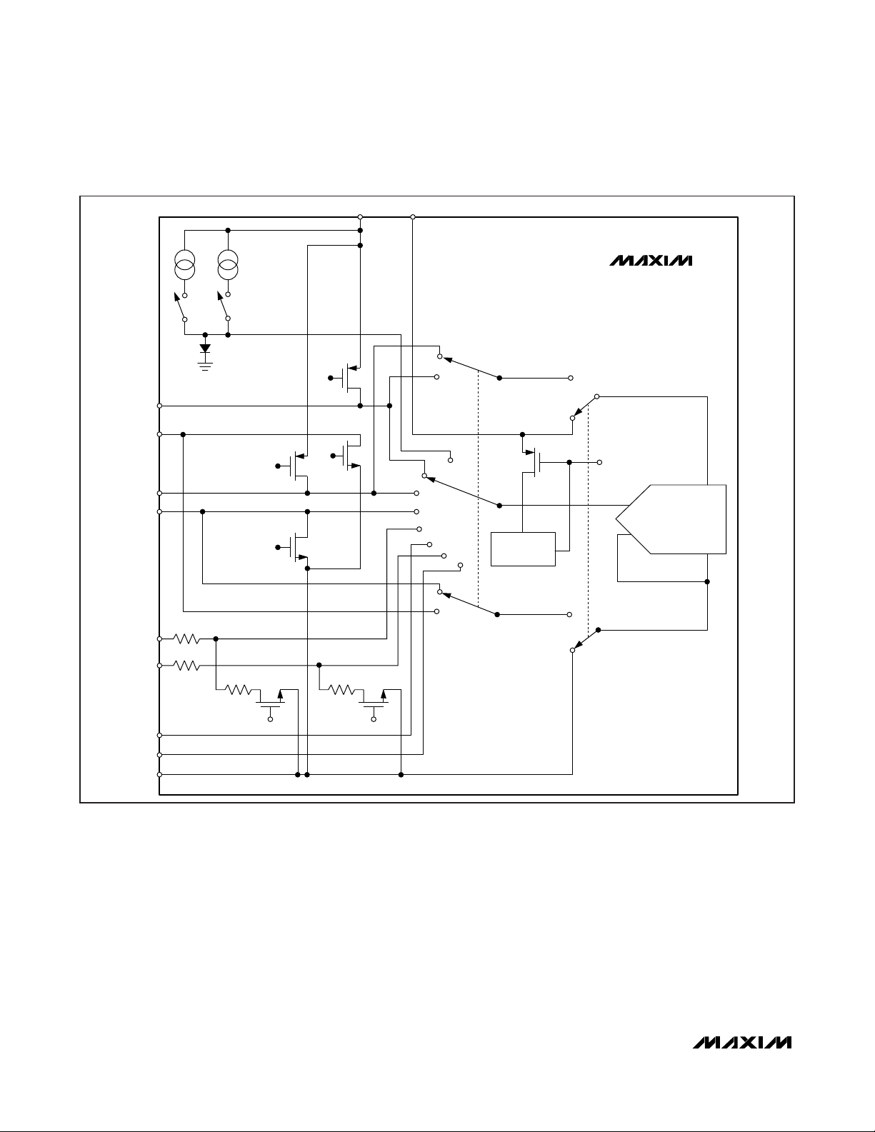
Touch-Screen Operation
The 4-wire touch-screen controller works by creating a
voltage gradient across the vertical or horizontal resistive touch screen connected to the analog inputs of the
MAX1233/MAX1234, as shown in Figure 2. The voltage
across the touch-screen panels is applied through internal MOSFET switches that connect each resistive layer
to AVDDand ground. For example, to measure the Y
position when a pointing device presses on the touch
screen, the Y+ and Y- drivers are turned on, connecting
one side of the vertical resistive layer to AVDDand the
other side to ground. The horizontal resistive layer functions as a sense line. One side of this resistive layer gets
connected to the X+ input, while the other side is left
open or floating. The point where the touch screen is
pressed brings the two resistive layers in contact and
creates a voltage-divider at that point. The data converter senses the voltage at the point of contact through the
X+ input and digitizes it.
12-Bit ADC
Analog Inputs
Figure 3 shows a block diagram of the ADC’s analog
input section including the input multiplexer, the differential input, and the differential reference. The input multiplexer switches between X+, X-, Y+, Y-, AUX1, AUX2,
BAT1, BAT2, and the internal temperature sensor.
The time required for the T/H to acquire an input signal
is a function of how quickly its input capacitance is
charged. If the input signal’s source impedance is high,
the acquisition time lengthens, and more time must be
allowed. The acquisition time (t
ACQ
) is the maximum
time the device takes to acquire the input signal to 12bit accuracy. Configure t
ACQ
by writing to the ADC
control register. See Table 1 for the maximum input signal source impedance (R
SOURCE
) for complete settling
during acquisition.
Accommodate higher source impedances by placing a
0.1µF capacitor between the analog input and GND.
Input Bandwidth
The ADC’s input-tracking circuitry has a 0.5MHz smallsignal bandwidth. To avoid high-frequency signals
being aliased into the frequency band of interest, antialias filtering is recommended.
Pin Description (continued)
*
ESD protected: ±8kV Contact, ±15kV Air.
PIN NAME FUNCTION
19 C2 Keypad Column 2. Can be reconfigured as GPIO5.
20 C3 Keypad Column 3. Can be reconfigured as GPIO6.
21 C4 Keypad Column 4. Can be reconfigured as GPIO7.
22 KEYIRQ Active-Low Keypad Interrupt. KEYIRQ is low when a key press is detected.
23 PENIRQ Active-Low Pen Touch Interrupt. PENIRQ is low when a screen touch is detected.
24 DOUT Serial Data Output. Data is clocked out at SCLK falling edge. High impedance when CS is high.
25 BUSY
26 DIN Serial Data Input. Data is clocked in on the rising edge of SCLK.
27 SCLK
28 CS
—EP
Active-Low Busy Output. BUSY goes low and stays low during each functional operation. The host
controller should wait until BUSY is high again before using the serial interface.
Serial Clock Input. Clocks data in and out of the serial interface and sets the conversion speed (duty
cycle must be 30% to 70%).
Active-Low Chip Select. Data is not clocked into DIN unless CS is low. When CS is high, DOUT is
high impedance.
Exposed Pad. Internally connected to GND. Connect to a large ground plane to maximize thermal
performance. Not intended as an electrical connection point.
Page 13
MAX1233/MAX1234
±15kV ESD-Protected Touch-Screen
Controllers Include DAC and Keypad Controller
______________________________________________________________________________________ 13
Figure 1. Block Diagram
Figure 2. Touch-Screen Measurement
Table 1. Maximum Input Source
Impedance
*X+
*Y+
*BAT1
*BAT2
*AUX1
*AUX2
REF
DACOUT
C1 C2 C3 C4 R1 R2 R3 R4
INTERNAL
REFERENCE
2.5V/1.0V
KEYPAD CONTROLLER
AND GPIO
REGISTERS AND
SCAN STATE
CONTROL
SERIAL
DATA
I/O
DOUT
SCLK
DIN
CS
PENIRQ
KEYIRQ
BUSY
OSCILLATOR
MAX1233
MAX1234
TEMP
SENSOR
*X-
*Y-
X/Y SWITCHES
BATTERY MONITOR
BATTERY MONITOR
8-BIT
DAC
REF
DAC
MUX
12-BIT
ADC
*ESD PROTECTED
+AV
FORCE LINE
Y+
SENSE LINE
X+
FORCE LINE
Y-
GND
DD
SENSE
LINE
ACQUISITION
TIME (µs)
1.5 8 2.6
1.5 10 2.0
+REF
+IN
-IN
-REF
1.5 12 1.5
5.0 8 23
5.0 10 19
5.0 12 15
95 8 560
95 10 470
95 12 400
RESOLUTION
(BITS)
MAXIMUM R
SOURCE
FOR
COMPLETE SETTLING
DURING ACQUISITION (kΩ)
Page 14
MAX1233/MAX1234
±15kV ESD-Protected Touch-Screen
Controllers Include DAC and Keypad Controller
14 ______________________________________________________________________________________
Analog Input Protection
Internal protection diodes that clamp the analog input
to AVDDand GND allow the analog input pins to swing
from GND - 0.3V to AVDD+ 0.3V without damage.
Analog inputs must not exceed AV
DD
by more than
50mV or be lower than GND by more than 50mV for
accurate conversions. If an off-channel analog input
voltage exceeds the supplies, limit the input current to
50mA. All analog inputs are also fully ESD protected
to ±8kV, using the Contact-Discharge method and
±15kV using the Air-Gap method specified in IEC1000-4-2.
Reference for ADC
Internal Reference
The MAX1233/MAX1234 offer an internal voltage reference for the ADC that can be set to +1.0V or +2.5V. The
MAX1233/MAX1234 typically use the internal reference
for battery monitoring, temperature measurement, and for
Figure 3. Simplified Diagram of Analog Input Section
TEMP1
TEMP2
X+
X-
Y+
Y-
+AV
DD
V
REF
MAX1233
MAX1234
REF ON/OFF
CONVERTER
+REF
-
REF
2.5V/1.0V
REFERENCE
+IN
-IN
7.5kΩ
V
BAT1
7.5kΩ
V
BAT2
AUX1
AUX2
GND
2.5kΩ
BATTERY
ON
2.5kΩ
BATTERY
ON
Page 15

MAX1233/MAX1234
±15kV ESD-Protected Touch-Screen
Controllers Include DAC and Keypad Controller
______________________________________________________________________________________ 15
measurement of the auxiliary inputs. Figure 4 shows the
on-chip reference circuitry of the MAX1233/MAX1234.
Set the internal reference voltage by writing to the RFV
bits in the ADC control register (see Tables 4, 5, and 12).
The MAX1233/MAX1234 can accept an external reference connected to REF for ADC conversion.
External Reference
The MAX1233/MAX1234 can accept an external reference connected to the REF pin for ADC conversions.
The internal reference should be disabled (RES1 = 1)
when using an external reference. At a conversion rate
of 50ksps, an external reference at REF must deliver up
to 15µA of load current and have 50Ω or less output
impedance. If the external reference has high output
impedance or is noisy, bypass it close to the REF pin
with a 0.1µF capacitor.
Selecting Internal or External Reference
Set the type of reference being used by programming
the ADC control register. To select the internal reference, clock zeros into bits [A/D3:A/D0] and a zero to bit
RES1, as shown in the
Control Registers
section. To
change to external reference mode, clock zeros into
bits [A/D3:A/D0] and a one to bit RES1. See Table 13
for more information about selecting an internal or
external reference for the ADC.
Reference Power Modes
Auto Power-Down Mode (RES1 = RES0 = 0)
The MAX1233/MAX1234 are in auto power-down mode
at initial power-up. Set the RES1 and RES0 bits to zero
to use the MAX1233/MAX1234 in the auto power-down
mode. In this mode, the internal reference is normally
off. When a command to perform a battery measure-
ment, temperature measurement, or auxiliary input
measurement is written to the ADC control register, the
device powers on the internal reference, waits for the
internal reference to settle, completes the requested
scan, and powers down the internal reference. The reference power delay depends upon the ADC resolution
selected (see Table 8). Do not bypass REF with an
external capacitor when performing scans in auto
power-down mode.
Full-Power Mode (RES1 = 0, RES0 = 1)
In the full-power mode, the RES1 bit is set LOW and
RES0 bit is set HIGH. In this mode, the device is powered up and the internal ADC reference is always ON.
The MAX1233/MAX1234 internal reference remains fully
powered after completing a scan.
Internal Clock
The MAX1233/MAX1234 operate from an internal oscillator, which is accurate to within 20% of the 10MHz
specified clock rate. The internal oscillator controls the
timing of the acquisition, conversion, touch-screen settling, reference power-up, and keypad debounce times.
8-Bit DAC
The MAX1233/MAX1234 have a voltage-output, true 8-bit
monotonic DAC with less than 1LSB integral nonlinearity
error and less than 1LSB differential nonlinearity error. It
requires a supply current of only 150µA (typ) and provides a buffered voltage output. The DAC is at midscale
code at power-up and remains there until a new code is
written to the DAC register. During shutdown, the DAC’s
output is pulled to ground with a 1MΩ load.
The internal DAC can be used in various system applications such as LCD/TFT-bias control, automatic tuning
(VCO), power amplifier bias control, programmable
threshold levels, and automatic gain control (AGC).
The 8-bit DAC in the MAX1233/MAX1234 employs a
current-steering topology as shown in Figure 5. At the
core of this DAC is a reference voltage-to-current converter (V/I) that generates a reference current. This current is mirrored to 255 equally weighted current
sources. DAC switches control the outputs of these current mirrors so that only the desired fraction of the total
current-mirror currents is steered to the DAC output.
The current is then converted to a voltage across a
resistor, and the output amplifier buffers this voltage.
DAC Output Voltage
The 8-bit DAC code is binary unipolar with 1LSB =
(V
REF
/256). The DAC has a full-scale output voltage of
(0.9 × AV
DD
- 1LSB).
Figure 4. Block Diagram of the Internal Reference
+1.25V
BANDGAP
3R
2R
2x
REF PIN
OPTIONAL
Page 16

MAX1233/MAX1234
±15kV ESD-Protected Touch-Screen
Controllers Include DAC and Keypad Controller
16 ______________________________________________________________________________________
Output Buffer
The DAC voltage output is an internally buffered unitygain follower that slews at up to ±0.4V/µs. The output
can swing from zero to full scale. With a 1/4FS to 3/4FS
output transition, the amplifier output typically settles to
1/2LSB in less than 5µs when loaded with 10kΩ in parallel with 50pF. The buffer amplifier is stable with any
combination of resistive loads >10kΩ and capacitive
loads <50pF.
Power-On Reset
All registers of the MAX1233/MAX1234 power up at a
default zero state, except the DAC data register, which
is set to 10000000, so the output is at midscale.
Keypad Controller and GPIO
The keypad controller is designed to interface a matrixtype 4 rows × 4 columns (16 keys or fewer) keypad to a
host controller. The KEY control register controls keypad
interrupt, keypad scan, and keypad debounce times.
The KeyMask and ColumnMask registers enable masking of a particular key or an entire column of the keypad
when they are not in use. The MAX1233/MAX1234 offer
two keypad data registers. KPData1 is the pending register. KPData2 holds keypad scan results of only the
unmasked keys. If 12 or fewer keys are being monitored,
one or more of the row/column pins of the
MAX1233/MAX1234 can be software programmed as
GPIO pins.
Touch-Screen Detection
Touch-screen detection can be enabled or disabled by
writing to the ADC control register as shown in Table 4.
Touch-screen detection is disabled at initial power-up.
Once touch-screen detection is enabled, the Y- driver
is on and the Y- pin is connected to GND. The X+ pin is
internally pulled to AVDDthrough a 1MΩ resistor as
shown in Figure 6. When the screen is touched, the X+
pin is pulled to GND through the touch screen and a
touch is detected.
When the 1MΩ pullup resistor is first connected, the X+
pin can be floating near ground. To prevent false touch
detection in this case, the X+ pin is precharged high for
0.1µs using the 7Ω PMOS driver before touch detection
begins.
Key-Press Detection
Key-press detection can be enabled or disabled by
writing to the keypad control register as shown in Table
17. Key-press detection is disabled at initial power-up.
Once key-press detection is enabled, the C_ pins are
internally connected to DV
DD
and the R_ pins are internally pulled to GND through a 16kΩ resistor. When a
key is pressed, the associated row pin is pulled to
DVDDand the key press is detected. Figure 7 shows
the key-press detection circuitry.
Interrupts
PEN Interrupt Request (PENIRQ)
The PENIRQ output can be used to alert the host controller of a screen touch. The PENIRQ output is normally
high and goes low after a screen touch is detected.
Figure 5. DAC Current-Steering Topology
Figure 6. Touch-Screen Detection Block Diagram
+AV
DD
V
REF
1MΩ
SW1 SW2
SW255
OUT
S1
TOUCH-SCREEN
TOUCH
SCREEN
X+
Y+
X-
Y-
S2
DETECTOR
PENIRQ
Page 17

MAX1233/MAX1234
±15kV ESD-Protected Touch-Screen
Controllers Include DAC and Keypad Controller
______________________________________________________________________________________ 17
Figure 7. Key-Press Detection Circuitry
Figure 8a. Timing Diagram for Touch-Initiated Screen Scan
Figure 8b. Timing Diagram for Host-Initiated Screen Scan
SIMPLIFIED KEYPAD CIRCUITRY
DRIVERS PULL HIGH
OR GO THREE-STATE
C1 C2 C3 C4
R1
TO KEYPAD
WAKEUP AND
DEBOUNCE
LOGIC
X+
PENIRQ
BUSY
KEYPAD
R2
R3
R4
X+
PENIRQ
BUSY
CS
DOUT
TOUCHSCREEN
DATA
DATA
READ
CS
DIN
DOUT
DATA
READ
TOUCHSCREEN
DATA
Page 18

MAX1233/MAX1234
±15kV ESD-Protected Touch-Screen
Controllers Include DAC and Keypad Controller
18 ______________________________________________________________________________________
PENIRQ returns high only after a touch-screen scan is
completed. PENIRQ does not go low again until one of
the touch-screen data registers is read. Figures 8a and
8b show the timing diagrams for the PENIRQ pin.
Keypad Interrupt Request (KEYIRQ)
The KEYIRQ output can be used to alert the host controller of a key press. The KEYIRQ output is normally
high and goes low after a key press is detected.
KEYIRQ returns high only after a key-press scan is
completed. KEYIRQ does not go low again until one of
the key-press data registers is read. Figures 9a and 9b
show the timing diagrams for the KEYIRQ pin.
Busy Indicator (
BUSY
)
BUSY informs the host processor that a scan is in
progress. BUSY is normally high and goes low and
stays low during each functional operation. The host
controller should wait until BUSY is high again before
using the serial interface.
Digital Interface
The MAX1233/MAX1234 interface to the host controller
through a standard 3-wire serial interface at up to
10MHz. DIN and CS are the digital inputs to the
MAX1233/MAX1234. DOUT is the serial data output.
Data is clocked out at the SCLK falling edge and is
high impedance when CS is high. When performing an
ADC scan, CS must de-assert high before the end of
the first conversion, otherwise the conversion results
will not be stored. PENIRQ and KEYIRQ communicate
interrupts from the touch-screen and keypad controllers
to the host processor when a screen touch or a key
press is detected. BUSY informs the host processor that
a scan is in progress. In addition to these digital I/Os, the
row and column pins of the keypad controller can be
programmed as GPIO pins.
Communications Protocol
The MAX1233/MAX1234 are controlled by reading from
and writing to registers through the 3-wire serial interface. These registers are addressed through a 16-bit
command that is sent prior to the data. The command
is shown in Table 2.
The first 16 bits after the falling edge of CS contain the
command word. The command word begins with an
R/W bit, which specifies the direction of data flow on
the serial bus. Bits 14 through 7 are reserved for future
use. Bit 6 specifies the page of memory in which the
desired register is located. The last 6 bits specify the
address of the desired register. The next 16 bits of data
are read from or written to the address specified in the
command word. After 32 clock cycles, the interface
automatically increments its address pointer and continues reading or writing until the rising edge of CS, or
until it reaches the end of the page.
Figure 9a. Timing Diagram for Key-Press-Initiated Debounce
Scan
Figure 9b. Timing Diagram for Host-Initiated Keypad
Debounce Scan
Table 2. Command Word Format
R_
KEYIRQ
BUSY
CS
DOUT
R_
KEYIRQ
BUSY
CS
DIN
DOUT
TOUCHSCREEN
DATA
TOUCHSCREEN
DATA
DATA
READ
DATA
READ
BIT15
BIT14 BIT13 BIT12 BIT11 BIT10 BIT9 BIT8 BIT7 BIT6 BIT5 BIT4 BIT3 BIT2 BIT1
MSB
R/W RES RES RES RES RES RES RES RES PAGE ADD5 ADD4 ADD3 ADD2 ADD1 ADD0
BIT0
LSB
Page 19

MAX1233/MAX1234
±15kV ESD-Protected Touch-Screen
Controllers Include DAC and Keypad Controller
______________________________________________________________________________________ 19
Table 3. Register Summary
Note: All other registers are reserved and should always be 0. Power-on reset state is DAC data at midscale (0x0080), all other reg-
isters are 0.
WRITE
COMMAND
0x000B 0x800B DAC data 0 0 0 0 0 0 0 0 DA7 DA6 DA5 DA4 DA3 DA2 DA1 DA0
0x000F 0x800F GPIO data GPD7 GPD6 GPD5 GPD4 GPD3 GPD2 GPD1 GPD0 0 0 0 00000
0x0040 0x8040 ADC control P EN STS ADSTS A/D3 A/D2 A/D1 A/D0 RES1 RES0 AVG1 AVG0 CNR1 CNR0 ST2 ST1 ST0 RFV
0x0041 0x8041 KEY control KEYSTS1 KEYSTS0 DB N2 D BN 1 DB N0 H LD 2 H LD 1 H LD 0 0 0 0 00000
0x0042 0x8042 DAC control DAPD 0 0 0 0 0 0 0 0 0 0 00000
0x004E 0x804E GPIO pullup PU7 PU6 PU5 PU4 PU3 PU2 PU1 PU0 0 0 0 00000
0x004F 0x804F GPIO control GP7 GP6 GP5 GP4 GP3 GP2 GP1 GP0 OE7 OE6 OE5 OE4 OE3 OE2 OE1 OE0
0x0050 0x8050 KPKeyMask KM15 KM14 KM13 KM12 KM11 KM10 KM9 KM8 KM7 KM6 KM5 KM4 KM3 KM2 KM1 KM0
0x0051 0x8051 KPColumnMask CM4 CM3 CM2 CM1 0 0 0 0 0 0 0 00000
READ
(HEX)
REGISTER
NAME
BIT15 BIT14 BIT13 BIT12 BIT11 BIT10 BIT9 BIT8 BIT7 BIT6 BIT5 BIT4 BIT3 BIT2 BIT1 BIT0
COMMAND
(HEX)
— 0x8000 X 0 0 0 0 X11 X10 X9 X8 X7 X6 X5 X4 X3 X2 X1 X0
— 0x8001 Y 0 0 0 0 Y11 Y10 Y9 Y8 Y7 Y6 Y5 Y4 Y3 Y2 Y1 Y0
— 0x8002 Z1 0 0 0 0 Z1_11 Z1_10 Z1_9 Z1_8 Z1_7 Z1_6 Z1_5 Z1_4 Z1_3 Z1_2 Z1_1 Z1_0
— 0x8003 Z2 0 0 0 0 Z2_11 Z2_10 Z2_9 Z2_8 Z2_7 Z2_6 Z2_5 Z2_4 Z2_3 Z2_2 Z2_1 Z2_0
— 0x8004 KPD K15 K14 K13 K12 K11 K10 K9 K8 K7 K6 K5 K4 K3 K2 K1 K0
— 0x8005 BAT1 0 0 0 0 B1_11 B1_10 B1_9 B1_8 B1_7 B1_6 B1_5 B1_4 B1_3 B1_2 B1_1 B1_0
— 0x8006 BAT2 0 0 0 0 B2_11 B2_10 B2_9 B2_8 B2_7 B2_6 B2_5 B2_4 B2_3 B2_2 B2_1 B2_0
— 0x8007 AUX1 0 0 0 0 A1_11 A1_10 A1_9 A1_8 A1_7 A1_6 A1_5 A1_4 A1_3 A1_2 A1_1 A1_0
— 0x8008 AUX2 0 0 0 0 A2_11 A2_10 A2_9 A2_8 A2_7 A2_6 A2_5 A2_4 A2_3 A2_2 A2_1 A2_0
— 0x8009 TEMP1 0 0 0 0 T1_11 T1_10 T1_9 T1_8 T1_7 T1_6 T1_5 T1_4 T1_3 T1_2 T1_1 T1_0
— 0x800A TEMP2 0 0 0 0 T2_11 T2_10 T2_9 T2_8 T2_7 T2_6 T2_5 T2_4 T2_3 T2_2 T2_1 T2_0
— 0x8010 KPData1 K1_15 K1_14 K1_13 K1_12 K1_11 K1_10 K1_9 K1_8 K1_7 K1_6 K1_5 K1_4 K1_3 K1_2 K1_1 K1_0
— 0x8011 KPData2 K2_15 K2_14 K2_13 K2_12 K2_11 K2_10 K2_9 K2_8 K2_7 K2_6 K2_5 K2_4 K2_3 K2_2 K2_1 K2_0
Page 20

MAX1233/MAX1234
±15kV ESD-Protected Touch-Screen
Controllers Include DAC and Keypad Controller
20 ______________________________________________________________________________________
In order to read the entire first page of memory, for
example, the host processor must send the
MAX1233/MAX1234 the command 0x8000
H
. The
MAX1233/MAX1234 then begin clocking out 16-bit data
starting with the X-data register. In order to write to the
second page of memory, the host processor sends the
MAX1233/MAX1234 the command 0x0040H. The succeeding data is then written in 16-bit words beginning
with the ADC control register. Figures 10a and 10b show
a complete write and read operation, respectively,
between the processor and the MAX1233/MAX1234.
Memory Map
The MAX1233/MAX1234s’ internal memory is divided
into two pages—one for data and one for control, each
of which contains thirty-two 16-bit registers.
Control Registers
Table 3 provides a summary of all registers and bit
locations of the MAX1233/MAX1234.
ADC Control Register
The ADC measures touch position, touch pressure, battery voltage, auxiliary analog inputs, and temperature.
The ADC control register determines which input is
selected and converted. Tables 4 and 5 show the format and bit descriptions for the ADC control register.
Figure 10a. Timing Diagram of Write Operation
Figure 10b. Timing Diagram of Read Operation
Table 4. ADC Control Register (Write 0x0040/Read 0x8040)
SCLK
CS
DIN
D15 IS READ/WRITE BIT
D15
LOW FOR WRITE
D15–D0 COMMAND WORD
WRITE OPERATION
D0
D15
D15–D0 DATA WORD
D0
THREE-
DOUT
STAT E
TIMING NOT TO SCALE.
SCLK
CS
DIN
DOUT
THREE-STATE
D15 D14
D15–D0 COMMAND
WORD
READ OPERATION
D0
D15
D0
D15
DATA WORD DATA WORD
THREE-
STAT E
D0
THREE-STATE
BIT15 BIT14 BIT13 BIT12 BIT11 BIT10 BIT9 BIT8 BIT7 BIT6 BIT5 BIT4 BIT3 BIT2 BIT1 BIT0
PENSTS ADSTS A/D3 A/D2 A/D1 A/D0 RES1 RES0 AVG1 AVG0 CNR1 CNR0 ST2 ST1 ST0 RFV
Page 21
MAX1233/MAX1234
±15kV ESD-Protected Touch-Screen
Controllers Include DAC and Keypad Controller
______________________________________________________________________________________ 21
Bits 14-15: Pen Interrupt Status and
ADC Status Bits
These bits are used to control or monitor ADC scans.
Bits 10-13: ADC Scan Select
These bits control which input to convert and which converter mode is used. The bits are identical regardless of a
read or write. See Table 7 for details about using these bits.
Bits 8-9: ADC Resolution Control
These bits specify the ADC resolution and are identical
regardless of read or write. Table 8 shows how to use
these bits to set the resolution.
Bits 6-7: Converter Averaging Control
These bits specify the number of data averages the
converter performs. Table 9 shows how to program for
the desired number of averages. When averaging is
used, ADSTS and BUSY indicate the converter is busy
until all conversions needed for the averaging finish.
These bits are identical, regardless of read or write.
Bits 4-5: ADC Conversion Rate Control
These bits specify the internal conversion rate, which
the ADC uses to perform a single conversion, as shown
in Table 10. Lowering the conversion rate also reduces
power consumption. These bits are identical, regardless of read or write.
Table 5. ADC Control Register Bit Descriptions (Write 0x0040/Read 0x8040)
Table 6. ADSTS Bit Operation
BIT NAME DESCRIPTION
15 (MSB) PENSTS Read: pen interrupt status; Write: sets interrupt initiated touch-screen scans
14 ADSTS Read: ADC status; Write: stops ADC
13 A/D3 Selects ADC scan functions
12 A/D2 Selects ADC scan functions
11 A/D1 Selects ADC scan functions
10 A/D0 Selects ADC scan functions
9 RES1 Controls ADC resolution
8 RES0 Controls ADC resolution
7 AVG1 Controls ADC result averaging
6 AVG0 Controls ADC result averaging
5 CNR1 Controls ADC conversion rate
4 CNR0 Controls ADC conversion rate
3 ST2 Controls touch-screen settling wait time
2 ST1 Controls touch-screen settling wait time
1 ST0 Controls touch-screen settling wait time
0 (LSB) RFV Chooses 1.0V or 2.5V reference
PENSTS ADSTS READ FUNCTION WRITE FUNCTION
00
10
01
11
No screen touch detected;
scan or conversion in progress
Screen touch detected;
scan or conversion in progress
No screen touch detected;
data available
Screen touch detected;
data available
Performs one scan and waits to detect a screen touch. Upon
detection, issues an interrupt and waits until told to scan by the
host controller.
Stops any ongoing scan and waits to detect a screen touch. Upon
detection, issues an interrupt and performs a scan.
Stops any ongoing scan and waits to detect a screen touch. Upon
detection, issues an interrupt and waits until told to scan by the
host controller.
Stops any ongoing scan and powers down the screen touch
detection circuit. No screen touches are detected in this mode.
Page 22

MAX1233/MAX1234
±15kV ESD-Protected Touch-Screen
Controllers Include DAC and Keypad Controller
22 ______________________________________________________________________________________
Table 7. ADC Scan Select (Touch Screen, Battery, Auxiliary Channels, and Temperature)
Table 8. ADC Resolution Control
*
Applicable only for temperature, battery, or auxiliary
measurements in auto power-up reference mode.
Table 9. ADC Averaging Control
Table 10. ADC Conversion Rate Control
A/D3 A/D2 A/D1 A/D0 FUNCTION
0000
0 0 0 1 Measures X/Y touch position and returns results to the X and Y data registers.
0010
0 0 1 1 Measures X touch position and returns results to the X data register.
0 1 0 0 Measures Y touch position and returns results to the Y data register.
0 1 0 1 Measures Z1/Z2 touch pressure and returns results to the Z1 and Z2 data register.
0 1 1 0 Measures Battery Input 1 through a 4:1 divider and returns results to the BAT1 data register.
0 1 1 1 Measures Battery Input 2 through a 4:1 divider and returns results to the BAT2 data register.
1 0 0 0 Measures Auxiliary Input 1 and returns results to the AUX1 data register.
1 0 0 1 Measures Auxiliary Input 2 and returns results to the AUX2 data register.
1 0 1 0 Measures temperature (single ended) and returns results to the TEMP1 data register.
1011
1 1 0 0 Measures temperature (differential) and returns results to the TEMP1 and TEMP2 data registers.
1 1 0 1 Turns on Y+, Y- drivers. No measurement is performed.
1 1 1 0 Turns on X+, X- drivers. No measurement is performed.
1 1 1 1 Turns on Y+, X- drivers. No measurement is performed.
Configures the ADC reference as selected by RES [1:0] bits as shown in Table 13. No measurement
is performed.
Measures X/Y touch position and Z1/ Z2 touch pressure and returns results to the X, Y, Z1, and Z2
data registers.
Measures Battery Input 1, Battery Input 2, Auxiliary Input 1, Auxiliary Input 2, and temperature
(differential), and returns results to the appropriate data registers.
RES1 RES0
0 0 8 bit 31
0 1 8 bit 31
1 0 10 bit 37
1 1 12 bit 44
ADC
RESOLUTION
INTERNALLY TIMED
REFERENCE POWER-UP
DELAY* (µs)
CNR1 CNR0 FUNCTION
00
01
10
11
3.5µs/sample
(1.5µs acquisition, 2µs conversion)
3.5µs/sample
(1.5µs acquisition, 2µs conversion)
10µs/sample
(5µs acquisition, 5µs conversion)
100µs/sample
(95µs acquisition, 5µs conversion)
AVG1 AVG0 FUNCTION
0 0 No data averages (default)
0 1 4 data averages
1 0 8 data averages
1 1 16 data averages
Page 23

MAX1233/MAX1234
±15kV ESD-Protected Touch-Screen
Controllers Include DAC and Keypad Controller
______________________________________________________________________________________ 23
Bits 1-3: Touch-Screen Settling Time Control
These bits specify the time delay from pen-touch detection to a conversion start. This allows the selection of the
appropriate settling time for the touch screen being used.
Table 11 shows how to set the settling time. These bits
are identical, regardless of read or write.
Bit 0: ADC Internal Reference Voltage Control
This bit selects the ADC internal reference voltage,
either +1.0V or +2.5V. This bit is identical, regardless of
read or write. The reference control bit is shown in
Table 12.
Internal ADC Reference Power-Down Control
The ADC control register controls the power setting of
the internal ADC reference. Zeros must be written to
bits A/D3–A/D0 to control internal reference power-up
followed by the appropriate logic at the RES1 and RES0
bits. Table 13 shows the internal ADC reference powerdown control.
DAC Control Register
The MSB in this control register determines the powerdown control of the on-board DAC. Table 14 shows the
DAC control register. Writing a zero to bit 15 (DAPD)
powers up the DAC, while writing a 1 powers down the
DAC. Table 15 describes the DAC control register contents, while Table 16 shows the DAC power-down bit.
Keypad Control Registers
The keypad control register, keypad mask register, and
keypad column mask control register control the keypad scanner in the MAX1233/MAX1234. The keypad
control register (Table 17) controls scanning and
debouncing, while the keypad mask register (Table 22)
and the keypad column mask control register (Table 24),
Table 11. Touch-Screen Settling Time
Control*
*
Applicable only for X, Y, Z1, and Z2 measurements.
Table 13. Internal ADC Reference Auto Power-Up Control
Table 12. ADC Reference Control Bit
Table 14. DAC Control Register (Write 0x0042/Read 0x8042)
BIT
DESCRIPTION
15 (MSB)
DAC powered down
[14:0]
0 Reserved
Table 15. DAC Control Register
Descriptions
DAPC FUNCTION
0 DAC powered up
1 DAC powered down
Table 16. DAC Power-Down Bit
ST2 ST1 ST0 SETTLING TIME
0 0 0 Settling time: 0µs
0 0 1 Settling time: 100µs
0 1 0 Settling time: 500µs
0 1 1 Settling time: 1ms
1 0 0 Settling time: 5ms
1 0 1 Settling time: 10ms
1 1 0 Settling time: 50ms
1 1 1 Settling time: 100ms
NAME
DAPD
RFV FUNCTION
0 +1.0V reference
1 +2.5V reference
[A/D3:A/D0] RES1 RES0
0000 0 0 Internal
0000 0 1 Internal Always powered up
0000 1 0 External Always powered down
0000 1 1 External Always powered down
A DC R EF ER EN C E
SOURCE
Power up, wait for reference to settle, and power down again for
each temperature, battery, or auxiliary scan (auto power-up mode)
ADC REFERENCE POWER MODE
BIT15 BIT14 BIT13 BIT12 BIT11 BIT10 BIT9 BIT8 BIT7 BIT6 BIT5 BIT4 BIT3 BIT2 BIT1 BIT0
DAPD000000000000000
Page 24
MAX1233/MAX1234
±15kV ESD-Protected Touch-Screen
Controllers Include DAC and Keypad Controller
24 ______________________________________________________________________________________
Table 19. KEYSTS1/KEYSTS0 Functions
Table 20. Keypad Debounce Time Control
Table 18. Keypad Control Register Bit Descriptions (Write 0x0041/Read 0x8041)
Table 17. Keypad Control Register (Write 0x0041/Read 0x8041)
BIT15 BIT14 BIT13 BIT12 BIT11 BIT10 BIT9 BIT8 BIT7 BIT6 BIT5 BIT4 BIT3 BIT2 BIT1 BIT0
KEYSTS1 KEYSTS0 DBN2 DBN1 DBN0 HLD2
BIT NAME DESCRIPTION
15 (MSB) KEYSTS1 Read: keypad interrupt status; Write: set interrupt initiated keypad scans
14 KEYSTS0 Read: keypad scan status; Write: stop keypad scan
13 DBN2 Keypad debounce time control
12 DBN1 Keypad debounce time control
11 DBN0 Keypad debounce time control
10 HLD2 Keypad hold time control
9 HLD1 Keypad hold time control
8 HLD0 Keypad hold time control
[7:0] 0 Reserved
KEYSTS1 KEYSTS0 READ FUNCTION WRITE FUNCTION
00
No button press detected;
scan or debounce in progress
HLD HLD
Scans keypad once and waits to detect a button press. Upon
detection, issues an interrupt and waits for the host’s instruction
before scanning.
00000000
10
01
11
Button press detected;
scan or debounce in progress
No button press detected;
data available
Button press detected;
data available
DBN2 DBN1 DBN0 FUNCTION (ms)
0 0 0 Debounce time: 2
0 0 1 Debounce time: 10
0 1 0 Debounce time: 20
0 1 1 Debounce time: 50
1 0 0 Debounce time: 60
1 0 1 Debounce time: 80
1 1 0 Debounce time: 100
1 1 1 Debounce time: 120
Stops any ongoing scan and waits to detect a button press. Upon
detection, issues an interrupt and scans the keypad.
Stops any ongoing scan and waits to detect a button press. Upon
detection, issues an interrupt and waits for the host’s instruction
before scanning.
Stops any ongoing scan and powers down the button press
detection circuit. No button presses are detected in this mode.
Page 25
Table 21. Keypad Hold Time Control
MAX1233/MAX1234
±15kV ESD-Protected Touch-Screen
Controllers Include DAC and Keypad Controller
______________________________________________________________________________________ 25
allowing certain keys to be masked from detection.
Tables 18–21 show the programmable bits of the keypad
control register. Tables 23, 24, and 25 show the programmable bits of the keypad mask registers. The
Keypad
Controller and GPIO
section provides more details.
GPIO Control Register
The GPIO control register and the GPIO pullup register
allow the keypad controller’s row and column inputs to be
configured as up to eight parallel I/O pins. Tables 26 and
27 show the GPIO control register layout and control register descriptions. Tables 28 and 29 show the GPIO pullup
disable register and associated descriptions. For more
information, see the
Applications Information
section.
Table 22. Keypad Key Mask Register Bit Descriptions (Write 0x0050/Read 0x8050)
Table 24. Keypad Column Mask Register (Write 0x0051/Read 0x8051)
Table 23. Keypad Key Mask Register Bit Descriptions (Write 0x0050/Read 0x8050)
HLD2 HLD1 HLD0 FUNCTION
0 0 0 If a button is held, wait 100µs before beginning next debounce scan
0 0 1 If a button is held, wait 1 debounce time before beginning the next debounce scan
0 1 0 If a button is held, wait 2 debounce times before beginning the next debounce scan
0 1 1 If a button is held, wait 3 debounce times before beginning the next debounce scan
1 0 0 If a button is held, wait 4 debounce times before beginning the next debounce scan
1 0 1 If a button is held, wait 5 debounce times before beginning the next debounce scan
1 1 0 If a button is held, wait 6 debounce times before beginning the next debounce scan
1 1 1 If a button is held, wait 7 debounce times before beginning the next debounce scan
BIT15 BIT14 BIT13 BIT12 BIT11 BIT10 BIT9 BIT8 BIT7 BIT6 BIT5 BIT4 BIT3 BIT2 BIT1 BIT0
KM15 KM14 KM13 KM12 KM11 KM10 KM9 KM8 KM7 KM6 KM5 KM4 KM3 KM2 KM1 KM0
BIT NAME DESCRIPTION
15 KM15 Mask status register data update on individual key for row 4, column 4
14 KM14 Mask status register data update on individual key for row 3, column 4
13 KM13 Mask status register data update on individual key for row 2, column 4
12 KM12 Mask status register data update on individual key for row 1, column 4
11 KM11 Mask status register data update on individual key for row 4, column 3
10 KM10 Mask status register data update on individual key for row 3, column 3
9 KM9 Mask status register data update on individual key for row 2, column 3
8 KM8 Mask status register data update on individual key for row 1, column 3
7 KM7 Mask status register data update on individual key for row 4, column 2
6 KM6 Mask status register data update on individual key for row 3, column 2
5 KM5 Mask status register data update on individual key for row 2, column 2
4 KM4 Mask status register data update on individual key for row 1, column 2
3 KM3 Mask status register data update on individual key for row 4, column 1
2 KM2 Mask status register data update on individual key for row 3, column 1
1 KM1 Mask status register data update on individual key for row 2, column 1
0 KM0 Mask status register data update on individual key for row 1, column 1
BIT15 BIT14 BIT13 BIT12 BIT11 BIT10 BIT9 BIT8 BIT7 BIT6 BIT5 BIT4 BIT3 BIT2 BIT1 BIT0
CM4CM3CM2CM1000000000000
Page 26

MAX1233/MAX1234
±15kV ESD-Protected Touch-Screen
Controllers Include DAC and Keypad Controller
26 ______________________________________________________________________________________
Data Registers
The data results from conversions or keypad scans are
held in the data registers of the MAX1233/MAX1234.
During power-up, all of these data registers with the
exception of the DAC data register default to 0000
H
.
The DAC register defaults to 1000
H
.
Analog Input Data Registers
Table 30 shows the format of the X, Y, Z1, Z2, BAT1,
BAT2, AUX1, AUX2, TEMP1, and TEMP2 data registers.
The data format for these registers is right justified
beginning with bit 11. Data written through the serial
interface to these registers is not stored.
Keypad Data Registers
Table 31 shows the formatting of the keypad data registers, while Tables 32, 33, and 34 provide individual register bit descriptions. These registers have the same
format as the keypad mask register. Each bit represents one key on the keypad. Table 35 shows a map of
a 16-key keypad. Data written through the serial interface to these registers is not stored.
Table 26. GPIO Control Register (Write 0x004F/Read 0x804F)
Table 27. GPIO Control Register Bit Descriptions (Write 0x004F/Read 0x804F)
Table 28.GPIO Pullup Disable Register (Write 0x004E/Read 0x804E)
Table 29. GPIO Pullup Disable Register
Descriptions
Table 25. Keypad Column Mask Register Bit Descriptions (Write 0x0051/Read 0x8051)
BIT NAME DESCRIPTION
15 CM4 Mask interrupt, status register, and pending register data update on all keys in column 4
14 CM3 Mask interrupt, status register, and pending register data update on all keys in column 3
13 CM2 Mask interrupt, status register, and pending register data update on all keys in column 2
12 CM1 Mask interrupt, status register, and pending register data update on all keys in column 1
[11:0] 0 Reserved
BIT15 BIT14 BIT13 BIT12 BIT11 BIT10 BIT9 BIT8 BIT7 BIT6 BIT5 BIT4 BIT3 BIT2 BIT1 BIT0
GP7 GP6 GP5 GP4 GP3 GP2 GP1 GP0 OE7 OE6 OE5 OE4 OE3 OE2 OE1 OE0
BIT NAME
15 GP7 C4 pin becomes GPIO pin 7 C4 pin remains keypad column 4
14 GP6 C3 pin becomes GPIO pin 6 C3 pin remains keypad column 3
13 GP5 C2 pin becomes GPIO pin 5 C2 pin remains keypad column 2
12 GP4 C1 pin becomes GPIO pin 4 C1 pin remains keypad column 1
11 GP3 R4 pin becomes GPIO pin 3 R4 pin remains keypad row 4
10 GP2 R3 pin becomes GPIO pin 2 R3 pin remains keypad row 3
9 GP1 R2 pin becomes GPIO pin 1 R2 pin remains keypad row 2
8 GP0 R1 pin becomes GPIO pin 0 R1 pin remains keypad row 1
[7:0] [OE7:OE0] GPIO pin configured as an output GPIO pin configured as an input
10
DESCRIPTION
BIT15 BIT14 BIT13 BIT12 BIT11 BIT10 BIT9 BIT8 BIT7 BIT6 BIT5 BIT4 BIT3 BIT2 BIT1 BIT0
PU7PU6PU5PU4PU3PU2PU1PU000000000
BIT NAME DESCRIPTION
[15:8] [PU7:PU0]
[7:0] 0 Reserved: always write as zero.
1: P ul l up d i sab l ed . Op en col l ector outp ut.
0: Pullup enabled.
Page 27

MAX1233/MAX1234
±15kV ESD-Protected Touch-Screen
Controllers Include DAC and Keypad Controller
______________________________________________________________________________________ 27
Table 30. Analog Inputs Data Register Format
Table 31. Keypad Data Registers
Table 32. Keypad Data Register Descriptions
READ
COMMAND
0x8000 X 0000X11X10X9X8X7X6X5X4X3X2X1X0
0x8001 Y 0000Y11Y10Y9Y8Y7Y6Y5Y4Y3Y2Y1Y0
0x8002 Z1 0000Z1_11Z1_10Z1_9Z1_8Z1_7Z1_6Z1_5Z1_4Z1_3Z1_2Z1_1Z 1_0
0x8003 Z1 0000Z2_11Z2_10Z2_9Z2_8Z2_7Z2_6Z2_5Z2_4Z2_3Z2_2Z2_1Z 2_0
0x8005 BATT1 0000B1_11B1_10B1_9B1_8B1_7B1_6B1_5B1_4B1_3B1_2B1_1B1_0
0x8006 BATT2 0000B2_11B2_10B2_9B2_8B2_7B2_6B2_5B2_4B2_3B2_2B2_1B2_0
0x8007 AUX1 0000A1_11A1_10A1_9A1_8A1_7A1_6A1_5A1_4A1_3A1_2A1_1A1_0
0x8008 AUX2 0000A2_11A2_10A2_9A2_8A2_7A2_6A2_5A2_4A2_3A2_2A2_1A2_0
0x8009 TEMP1 0000T1_11T1_10T1_9T1_8T1_7T1_6T1_5T1_4T1_3T1_2T1_1T1_0
0x800A TEMP2 0000T2_11T2_10T2_9T2_8T2_7T2_6T2_5T2_4T2_3T2_2T2_1T2_0
READ
COMMAND
0x8004 KPD K15 K14 K13 K12 K11 K10 K9 K8 K7 K6 K5 K4 K3 K2 K1 K0
0x8010
0x8011
REGI STER
NAME
REGISTER
NAME
KPData1
(column
m askabl e)
KPData2
(key
m askabl e)
BIT15 BIT14 BIT13 BIT12 BIT11 BIT10 BIT9 BIT8 BIT7 BIT6 BIT5 BIT4 BIT3 BIT2 BIT1 BIT0
BIT15 BIT14 BIT13 BIT12 BIT11 BIT10 BIT9 BIT8 BIT7 BIT6 BIT5 BIT4 BIT3 BIT2 BIT1 BIT0
K1_15 K1_14 K1_13 K1_12 K1_11 K1_10 K1_9 K1_8 K1_7 K1_6 K1_5 K1_4 K1_3 K1_2 K1_1 K1_0
K2_15 K2_14 K2_13 K2_12 K2_11 K2_10 K2_9 K2_8 K2_7 K2_6 K2_5 K2_4 K2_3 K2_2 K2_1 K2_0
BIT NAME DESCRIPTION
15 K15 Keypad scan result for row 4, column 4. Can only be masked by column mask.
14 K14 Keypad scan result for row 3, column 4. Can only be masked by column mask.
13 K13 Keypad scan result for row 2, column 4. Can only be masked by column mask.
12 K12 Keypad scan result for row 1, column 4. Can only be masked by column mask.
11 K11 Keypad scan result for row 4, column 3. Can only be masked by column mask.
10 K10 Keypad scan result for row 3, column 3. Can only be masked by column mask.
9 K9 Keypad scan result for row 2, column 3. Can only be masked by column mask.
8 K8 Keypad scan result for row 1, column 3. Can only be masked by column mask.
7 K7 Keypad scan result for row 4, column 2. Can only be masked by column mask.
6 K6 Keypad scan result for row 3, column 2. Can only be masked by column mask.
5 K5 Keypad scan result for row 2, column 2. Can only be masked by column mask.
4 K4 Keypad scan result for row 1, column 2. Can only be masked by column mask.
3 K3 Keypad scan result for row 4, column 1. Can only be masked by column mask.
2 K2 Keypad scan result for row 3, column 1. Can only be masked by column mask.
1 K1 Keypad scan result for row 2, column 1. Can only be masked by column mask.
0 K0 Keypad scan result for row 1, column 1. Can only be masked by column mask.
Page 28

MAX1233/MAX1234
±15kV ESD-Protected Touch-Screen
Controllers Include DAC and Keypad Controller
28 ______________________________________________________________________________________
Table 33. Keypad Data Register 1 (Pending Register) Descriptions
Table 34. Keypad Data Register 2 (Status Register) Descriptions
BIT NAME DESCRIPTION
15 K1_15 Keypad scan result for row 4, column 4. Can only be masked by column mask.
14 K1_14 Keypad scan result for row 3, column 4. Can only be masked by column mask.
13 K1_13 Keypad scan result for row 2, column 4. Can only be masked by column mask.
12 K1_12 Keypad scan result for row 1, column 4. Can only be masked by column mask.
11 K1_11 Keypad scan result for row 4, column 3. Can only be masked by column mask.
10 K1_10 Keypad scan result for row 3, column 3. Can only be masked by column mask.
9 K1_9 Keypad scan result for row 2, column 3. Can only be masked by column mask.
8 K1_8 Keypad scan result for row 1, column 3. Can only be masked by column mask.
7 K1_7 Keypad scan result for row 4, column 2. Can only be masked by column mask.
6 K1_6 Keypad scan result for row 3, column 2. Can only be masked by column mask.
5 K1_5 Keypad scan result for row 2, column 2. Can only be masked by column mask.
4 K1_4 Keypad scan result for row 1, column 2. Can only be masked by column mask.
3 K1_3 Keypad scan result for row 4, column 1. Can only be masked by column mask.
2 K1_2 Keypad scan result for row 3, column 1. Can only be masked by column mask.
1 K1_1 Keypad scan result for row 2, column 1. Can only be masked by column mask.
0 K1_0 Keypad scan result for row 1, column 1. Can only be masked by column mask.
BIT NAME DESCRIPTION
15 K2_15 Keypad scan result for row 4, column 4. Can be masked by key mask or column mask.
14 K2_14 Keypad scan result for row 3, column 4. Can be masked by key mask or column mask.
13 K2_13 Keypad scan result for row 2, column 4. Can be masked by key mask or column mask.
12 K2_12 Keypad scan result for row 1, column 4. Can be masked by key mask or column mask.
11 K2_11 Keypad scan result for row 4, column 3. Can be masked by key mask or column mask.
10 K2_10 Keypad scan result for row 3, column 3. Can be masked by key mask or column mask.
9 K2_9 Keypad scan result for row 2, column 3. Can be masked by key mask or column mask.
8 K2_8 Keypad scan result for row 1, column 3. Can be masked by key mask or column mask.
7 K2_7 Keypad scan result for row 4, column 2. Can be masked by key mask or column mask.
6 K2_6 Keypad scan result for row 3, column 2. Can be masked by key mask or column mask.
5 K2_5 Keypad scan result for row 2, column 2. Can be masked by key mask or column mask.
4 K2_4 Keypad scan result for row 1, column 2. Can be masked by key mask or column mask.
3 K2_3 Keypad scan result for row 4, column 1. Can be masked by key mask or column mask.
2 K2_2 Keypad scan result for row 3, column 1. Can be masked by key mask or column mask.
1 K2_1 Keypad scan result for row 2, column 1. Can be masked by key mask or column mask.
0 K2_0 Keypad scan result for row 1, column 1. Can be masked by key mask or column mask.
Page 29

MAX1233/MAX1234
±15kV ESD-Protected Touch-Screen
Controllers Include DAC and Keypad Controller
______________________________________________________________________________________ 29
DAC Data Register
The DAC data register stores data that is to be written
to the 8-bit DAC. Table 36 shows the configuration of
the DAC data register. It is right justified with bit 7–bit 0
storing the input data.
GPIO Data Register
Tables 37 and 38 show the format and descriptions for
the GPIO data register. The register is left justified with
data in bit 15–bit 8. Reading the GPIO data register
gives the state of the R_ and C_ pins. Data written to
the GPIO data register appears on those R_ and C_
pins, which are configured as general-purpose outputs.
Data written to pins not configured as general-purpose
outputs is not stored.
ADC Transfer Function
The MAX1233/MAX1234 output data is in straight binary format as shown in Figure 11. This figure shows the
ideal output code for the given input voltage and does
not include the effects of offset error, gain error, noise,
or nonlinearity.
Applications Information
Programmable 8-/10-/12-Bit Resolution
The MAX1233/MAX1234 provide the option of three different resolutions for the ADC: 8, 10, or 12 bits. Lower
resolutions are practical for some measurements such
as touch pressure. Lower resolution conversions have
smaller conversion times and therefore consume less
power. Program the resolution of the MAX1233/
MAX1234 12-bit ADCs by writing to the RES1 and RES0
bits in the ADC control register. When the MAX1233/
MAX1234 power up, both bits are set to zero so the resolution is set to 8 bits with a 31µs internally timed reference power-up delay as indicated by the ADC
resolution control table. As explained in the control register section, the RES1 and RES0 bits control the refer-
Table 35. Keypad to Key Bit Mapping
Table 36. DAC Data Register(Write 0x000B/Read 0x800B)
Table 37. GPIO Data Register (Write 0x000F/Read 0x800F)
Table 38. GPIO Data Register Bit Descriptions (Write 0x000F/Read 0x800F)
Figure 11. Ideal Input Voltages and Output Codes
COMPONENT C1 C2 C3 C4
R1 K0 K4 K8 K12
R2 K1 K5 K9 K13
R3 K2 K6 K10 K14
R4 K3 K7 K11 K15
OUTPUT CODE
11 ... 111
11 ... 110
11 ... 101
00 ... 011
00 ... 010
00 ... 001
00 ... 000
FULL-SCALE
TRANSITION
30FS
21
INPUT VOLTAGE (LSB)
MAX1233
MAX1234
FS = V
ZS = GND
1LSB =
FS - 3/2LSB
REF
V
4096
REF
BIT15 BIT14 BIT13 BIT12 BIT11 BIT10 BIT9 BIT8 BIT7 BIT6 BIT5 BIT4 BIT3 BIT2 BIT1 BIT0
00000000DA7DA6DA5DA4DA3DA2DA1DA0
BIT15 BIT14 BIT13 BIT12 BIT11 BIT10 BIT9 BIT8 BIT7 BIT6 BIT5 BIT4 BIT3 BIT2 BIT1 BIT0
GPD7GPD6GPD5GPD4GPD3GPD2GPD1GPD000000000
BIT NAME DESCRIPTION
15...8 GPD7...0 GPIO data bits for GPIO pins 7...0
7...0 0 Reserved
Page 30

MAX1233/MAX1234
±15kV ESD-Protected Touch-Screen
Controllers Include DAC and Keypad Controller
30 ______________________________________________________________________________________
ence power-up status when the A/D0–A/D3 bits are
zero. These values can be set initially on power-up.
(Subsequently A/D0–A/D3 bits are not zero, and any
other value of these bits is exclusive to ADC resolution
programming.)
Differential Ratiometric Touch-Position
Measurement
The MAX1233/MAX1234 provide differential conversions. Figure 12 shows the switching matrix configuration for Y coordinate measurement. The +REF and -REF
inputs are connected directly to Y+ and Y-. The conversion result is a percentage of the external resistances,
and is unaffected by variation in the total touch-screen
resistance or the on-resistance of the internal switching
matrix. The touch screen remains powered during the
acquisition and conversion process.
Touch-Screen Settling
There are two mechanisms that affect the voltage level
at the point where the touch panel is pressed. One is
electrical ringing due to parasitic capacitance between
the top and bottom layers of the touch screen and the
other is the mechanical bouncing caused by vibration
of the top layer of the touch screen. Thus, the input sig-
nal, reference, or both may not settle into their final
steady-state values before the ADC samples the inputs,
and the reference voltage may continue to change during the conversion cycle. The MAX1233/MAX1234 can
be programmed to wait for a fixed amount of time after
a screen touch has been detected before beginning a
scan. Use the touch-screen settling control bits in the
ADC control register (Table 11) to set the settling delay
to between zero and 100ms.
The settling problem is amplified in some applications
where external filter capacitors may be required across
the touch screen to filter noise that may be generated
by the LCD panel or backlight circuitry, etc. The values
of these capacitors cause an additional settling time
requirement when the panel is touched. Any failure to
settle before conversion start may show up as a gain
error. Average the conversion result by writing to the
ADC control register, as shown in Table 10, to minimize
noise.
Touch-Pressure Measurement
The MAX1233/MAX1234 provide two methods of measurement of the pressure applied to the touch screen.
Although 8-bit resolution is typically sufficient, the following calculations use 12-bit resolution demonstrating the
maximum precision of the MAX1233/MAX1234. Figure 13
shows the pressure measurement block diagram.
The first method performs pressure measurements
using a known X-plate resistance. After completing
three conversions, X-position, Z1-position, and Z2 position, use the following equation to calculate R
TOUCH
:
The second method requires knowing both the X-plate
and Y-plate resistance. Three touch-screen conversions are required in this method as well for measurement of the X-position, Y-position, and Z- position of the
touch screen. Use the following equation to calculate
R
TOUCH
:
R
R
Z
X
Z
R
Y
TOUCH
XPLATE POSITION
YPLATE
POSITION
=
⎛
⎝
⎜
⎞
⎠
⎟
×
⎛
⎝
⎜
⎞
⎠
⎟
×
⎛
⎝
⎜
⎞
⎠
⎟
−
⎡
⎣
⎢
⎢
⎤
⎦
⎥
⎥
⎧
⎨
⎪
⎩
⎪
⎫
⎬
⎪
⎭
⎪
−×
⎛
⎝
⎜
⎞
⎠
⎟
⎧
⎨
⎪
⎩
⎪
⎫
⎬
⎪
⎭
⎪
11
4096
4096
1
4096
RR
XZ
Z
TOUCH XPLATE
POSITION
=
()
×
⎛
⎝
⎜
⎞
⎠
⎟
×
⎛
⎝
⎜
⎞
⎠
⎟
−
⎡
⎣
⎢
⎢
⎤
⎦
⎥
⎥
4096
1
2
1
Figure 12. Ratiometric Y-Coordinate Measurement
+AV
DD
FORCE LINE
Y+
X+
SENSE LINE
+IN
-IN
SENSE LINE
+REF
CONVERTER
-REF
FORCE LINE
Y-
GND
Page 31

Battery-Voltage Monitors
Two dedicated analog inputs (BAT1 and BAT2) allow the
MAX1233/MAX1234 to monitor the battery voltages prior
to the DC/DC converter. Figure 14 shows the battery voltage monitoring circuitry. The MAX1233/ MAX1234 directly monitor battery voltages from 0.5V to 6V. An internal
resistor network divides down BAT1 and BAT2 by 4 so
that a 6V battery voltage results in a 1.5V input to the
ADC. To minimize power consumption, the divider is only
enabled during the sampling of BAT1 and BAT2. Figure
15 illustrates the process of battery input reading.
MAX1233/MAX1234
±15kV ESD-Protected Touch-Screen
Controllers Include DAC and Keypad Controller
______________________________________________________________________________________ 31
Figure 13. Pressure Measurement Block Diagram
Figure 14. Battery Measurement Block Diagram
Figure 15. Battery Voltage-Reading Flowchart
FORCE LINE SENSE LINE
X+
V
FORCE LINE
MEASURE Z1-RESISTANCE
OPEN CIRCUIT
FORCE LINE
TOUCH
X-POSITION
X-
FORCE LINE
X+
TOUCH
Z2-RESISTANCE
X-
Y+
Y-
OPEN CIRCUIT
X+
TOUCH
Z1-RESISTANCE
X-
FORCE LINE
Y+
Y-
SENSE LINE
MEASURE X-POSITION
FORCE LINESENSE LINE
Y+
Y-
OPEN CIRCUIT
V
MEASURE Z2-RESISTANCE
HOST WRITES
ADC
CONTROL REGISTER
START CLOCK
SET BUSY
LOW
NO
V
NO
IS ADC
REFERENCE IN
AUTO POWER-DOWN
MODE?
YES
POWER UP REFERENCE
POWER UP
ADC
CONVERT
BATTERY INPUT 1 OR 2
IS DATA
AVERAGING DONE?
BATTERY INPUT 1 OR
BATTERY INPUT 2
POWER DOWN
ADC
POWER DOWN REFERENCE
SET BUSY HIGH
TURN OFF CLOCK
2.7V
CONVERTER
AV
DD
BATTERY
0.5V TO
6.0V
V
BAT
DC/DC
CONVERTER
7.5kΩ
0.125V TO 1.5V
2.5kΩ
YES
STORE BATTERY INPUT 1 OR 2 IN
BAT1 OR BAT2 REGISTER
DONE
Page 32

MAX1233/MAX1234
±15kV ESD-Protected Touch-Screen
Controllers Include DAC and Keypad Controller
32 ______________________________________________________________________________________
Auxiliary Analog Inputs
Two auxiliary analog inputs (AUX1 and AUX2) allow the
MAX1233/MAX1234 to monitor analog input voltages
from zero to V
REF
. Figure 16 illustrates the process of
auxiliary input reading.
Temperature Measurements
The MAX1233/MAX1234 provide two temperature measurement options: a single-ended conversion method
and a differential conversion method. Both temperature
measurement techniques rely on the semiconductor
junction’s operational characteristics at a fixed current
level. The forward diode voltage (VBE) vs. temperature is
a well-defined characteristic. The ambient temperature
can be predicted in applications by knowing the value
of the V
BE
voltage at a fixed temperature and then monitoring the delta of that voltage as the temperature
changes. Figure 17 illustrates the functional block of the
internal temperature sensor.
The single conversion method requires calibration at a
known temperature, but only requires a single reading to
predict the ambient temperature. First, the internal diode
forward bias voltage is measured by the ADC at a
known temperature. Subsequent diode measurements
provide an estimate of the ambient temperature through
extrapolation. This assumes a temperature coefficient of
-2.1mV/°C. The single conversion method results in a
resolution of 0.29°C/LSB (2.5V reference) and
0.12°C/LSB (1.0V reference) with a typical accuracy of
±2°C. Figure 18 shows the flowchart for the single temperature measurement.
The differential conversion method uses two measurement points. The first measurement is performed with a
fixed bias current into the internal diode. The second
measurement is performed with a fixed multiple of the
original bias current. The voltage difference between the
first and second conversion is proportional to the
absolute temperature and is expressed by the following
formula:
ΔV
BE
= (kT/q) ✕ ln(N)
where:
ΔVBE= difference in diode voltage
N = current ratio of the second measurement to the first
measurement
k = Boltzmann’s constant (1.38 × 10
-23
eV/°Kelvin)
q = electron charge (1.60 × 10
-19
C)
T = temperature in °Kelvin
The resultant equation solving for °K is:
T(°K) = q x ΔV / (k × ln(N))
Figure 16. Auxiliary Input Flowchart
Figure 17. Internal Block Diagram of Temperature Sensor
HOST WRITES
ADC
CONTROL REGISTER
START CLOCK
SET BUSY
LOW
NO
NO
STORE AUXILIARY INPUT 1 OR 2 IN
TEMP1 TEMP2
IS ADC
REFERENCE IN
AUTO POWER-DOWN
MODE?
YES
POWER UP REFERENCE
POWER UP
ADC
CONVERT
AUXILIARY INPUT 1 OR 2
IS DATA
AVERAGING DONE?
YES
AUX1 OR AUX2 REGISTER
AUXILIARY INPUT 1 OR
AUXILIARY INPUT 2
POWER DOWN
ADC
POWER DOWN REFERENCE
SET BUSY HIGH
TURN OFF CLOCK
DONE
MUX
A/D
CONVERTER
Page 33

MAX1233/MAX1234
±15kV ESD-Protected Touch-Screen
Controllers Include DAC and Keypad Controller
______________________________________________________________________________________ 33
where:
ΔV = V (I N) - V (I1) (in mV)
T(°K) = 2.68(°K/mV) ×ΔV(mV)
T(°C) = [2.68(°K/mV) ×ΔV(mV) - 273°K]°C/ °K
This differential conversion method does not require a
test temperature calibration and can provide much
improved absolute temperature measurement. In the
differential conversion method, however, the resolution
is 1.6°C/LSB (2.5V reference) and 0.65°C/LSB (1V reference) with a typical accuracy of ±3°C. Figure 19
shows the differential temperature measurementprocess.
Note: The bias current for each diode temperature
measurement is only turned ON during the acquisition
and, therefore, does not noticeably increase power
consumption.
Figure 18. Single Temperature Measurement Process
Figure 19. Differential Temperature Measurement Process
HOST WRITES
CONTROL REGISTER
START CLOCK
NO
REFERENCE IN
AUTO POWER-DOWN
POWER UP REFERENCE
TEMPERATURE INPUT 1
ADC
SET BUSY
LOW
IS ADC
MODE?
YES
POWER UP
ADC
CONVERT
TEMPERATURE INPUT 1
POWER DOWN
ADC
POWER DOWN REFERENCE
HOST WRITES
CONTROL REGISTER
START CLOCK
NO
REFERENCE IN
AUTO POWER-DOWN
POWER UP REFERENCE
TEMPERATURE INPUT 1
ADC
SET BUSY
LOW
IS ADC
MODE?
YES
POWER UP
ADC
CONVERT
TEMPERATURE INPUT 1
AND TEMPERATURE INPUT 2
CONVERT
TEMPERATURE INPUT 2
NO
STORE TEMPERATURE INPUT 2 IN
IS DATA
AVERAGING DONE?
YES
TEMP2 REGISTER
POWER DOWN
ADC
POWER DOWN REFERENCE
SET BUSY HIGH
NO
STORE TEMPERATURE INPUT 1 IN
IS DATA
AVERAGING DONE?
YES
TEMP1 REGISTER
TURN OFF CLOCK
DONE
SET BUSY HIGH
NO
STORE TEMPERATURE INPUT 1 IN
IS DATA
AVERAGING DONE?
YES
TEMP1 REGISTER
TURN OFF CLOCK
DONE
Page 34

MAX1233/MAX1234
±15kV ESD-Protected Touch-Screen
Controllers Include DAC and Keypad Controller
34 ______________________________________________________________________________________
Battery Voltage, Auxiliary Input, and
Temperature Input Scan
Use this scan to make periodic measurements of both
battery inputs, both auxiliary inputs, and both temperature inputs. The respective data registers have the latest results at the end of each cycle. Thus, a single write
by the host to the MAX1233/MAX1234 ADC control register results in six different measurements being made.
Figure 20 shows this scan operation.
Touch-Initiated Screen Scans
(PENSTS = 1; ADSTS = 0)
In the touch-initiated screen-scan mode, the
MAX1233/MAX1234 automatically perform a touchscreen scan upon detecting a screen touch. The touchscreen scans performed are determined by the
[A/D3:A/D0] written to the ADC control register. Figure
21 shows the flowchart for a complete touch-initiated Xand Y- coordinate scan. Selection of resolution, conversion rate, averaging, and touch-screen settling time
determine the overall conversion time.
Figure 22 shows the complete flowchart for a touchinitiated X, Y, and Z scan.
Table 38 shows ADSTS Bit Operation.
Host-Initiated Screen Scans
(PENSTS = ADSTS = 0)
In this mode, the host processor decides when a touchscreen scan begins. The MAX1233/MAX1234 detect a
screen touch and drive PENIRQ LOW. The host recognizes the interrupt request and can choose to write to
the ADC control register to select a touch-screen scan
function (PENSTS = ADSTS = 0). Figures 23 and 24
show the process of a host-initiated screen scan.
Key-Press Initiated Debounce Scan
(KEYSTS1 = 1, KEYSTS0 =0)
In the key-press initiated debounce mode, the
MAX1233/MAX1234 automatically perform a debounce
upon detecting a key press. Key scanning begins once
a key press has been detected and ends when a key
press has been debounced (Figures 25 and 9a).
Host-Initiated Debounce Scan
In this mode, the host processor decides when a
debounce scan begins. The MAX1233/MAX1234 detect
a key press and drive KEYIRQ low. The host processor
recognizes the interrupt request and can choose to
write to the keypad control register to initiate a
debounce scan (Figures 26 and 9b).
Keypad Debouncing
Keys are debounced either when (1) a key press has
been detected, or (2) when commanded by the host MPU.
The keys scanned by the keypad row and column pins
are debounced for a period of time (debounce period)
as determined by bits [DBN2:DBN0] of the keypad control register.
The keypad controller continues scanning until the keypad
stays in the same state for an entire debounce period.
Keypad Data
Keypad data can be read out of either the keypad data
status register (maskable), or the keypad data pending
register (not maskable). The keypad mask register is
used to mask individual keys in the keypad data status
register.
GPIO Control
Write to bits [GP7:GP0] of the GPIO control register to
configure one or more of the R_/C_pins as a GPIO pin.
Write to bits [OE7:OE0] of the GPIO control register to
configure the pins as an input or an output. GPIO data
can be read from or written to the GPIO data register. A
read returns the logic state of the GPIO pin. A write sets
the logic state of a GPIO output pin. Writing to a GPIO
input pin has no effect.
GPIO Pullup Disable Register
When programmed as GPIO output, by default, the
GPIO pins are active CMOS outputs. Write a 1 to the
pullup disable register to configure the GPIO output as
an open-drain output.
Using the 8-Bit DAC for LCD/TFT
Contrast Control
Design Example:
The 8-bit DAC offers the ability to control biasing of
LCD/TFT screens. In the circuit of Figure 27, it is
desired to have the MAX1677 DC-DC converter’s V
OUT
to be adjustable.
The minimum and maximum DAC voltages (V
DAC(HIGH)
and V
DAC(LOW)
) can be found in the
Electrical
Characteristics
table.
The output voltage of the MAX1677 (V
OUT
) can be cal-
culated by noting the following equations:
V
OUT
= V
REFDAC
+ i1R1 [Equation 1]
i1= i2+ i
3
[Equation 2]
i
2
= V
REFDAC
/ R2 [Equation 3]
i
3
= (V
REFDAC
- V
DAC
) / R3 [Equation 4]
Substituting equations 2, 3, and 4 into equation 1
yields:
V
OUT
= V
REFDAC
+ (R1 / R2) V
REF
+ (R1 / R3)
(V
REFDAC
- V
DAC
) [Equation 5]
Page 35

MAX1233/MAX1234
±15kV ESD-Protected Touch-Screen
Controllers Include DAC and Keypad Controller
______________________________________________________________________________________ 35
Figure 20. Scan Mode Flowchart
BATTERY VOLTAGE, AUXILIARY INPUT, AND TEMPERATURE INPUT SCAN ([A/D3:A/D0] = 1011)
HOST WRITES
ADC
CONTROL REGISTER
START CLOCK
CONVERT
BATTERY INPUT 2
CONVERT
TEMPERATURE INPUT 1
NO
AUTO POWER-DOWN
POWER UP REFERENCE
BATTERY INPUT 1
NO
AVERAGING DONE?
SET BUSY
LOW
IS ADC
REFERENCE IN
MODE?
YES
POWER UP
ADC
CONVERT
IS DATA
NO
NO
IS DATA
AVERAGING DONE?
YES
STORE BATTERY INPUT 2 IN
BAT2 REGISTER
CONVERT
AUXILIARY INPUT 1
IS DATA
AVERAGING DONE?
YES
STORE AUXILIARY INPUT 1 IN
AUX1 REGISTER
CONVERT
AUXILIARY INPUT 2
NO
STORE TEMPERATURE INPUT 1 IN
NO
STORE TEMPERATURE INPUT 2 IN
IS DATA
AVERAGING DONE?
YES
TEMP1 REGISTER
CONVERT
TEMPERATURE INPUT 2
IS DATA
AVERAGING DONE?
YES
TEMP2 REGISTER
POWER DOWN
ADC
STORE BATTERY INPUT 1 IN
BAT1 REGISTER
YES
NO
IS DATA
AVERAGING DONE?
YES
STORE AUXILIARY INPUT 2 IN
AUX2 REGISTER
POWER DOWN REFERENCE
SET BUSY HIGH
TURN OFF CLOCK
DONE
Page 36

MAX1233/MAX1234
±15kV ESD-Protected Touch-Screen
Controllers Include DAC and Keypad Controller
36 ______________________________________________________________________________________
Figure 21. Touch-Initiated X- and Y- Coordinate Screen Scan
PENIRQ-INITIATED
X- AND Y- SCREEN SCAN
SCREEN
TOUCH
POWER DOWN ADC
YES
ARE THERE
UNREAD SCAN
RESULTS?
SET
PENIRQ LOW
IS PENSTS
BIT = 1?
START CLOCK
SET BUSY LOW
TURN ON DRIVERS: Y+, Y-
NO
IS TOUCH-SCREEN
SETTLING DONE?
NO
YES
YES
HOST-INITIATED
NO
(FIGURE 23)
GO TO
SCAN
TURN ON DRIVERS: X+. X-
NO
IS TOUCH-SCREEN
SETTLING DONE?
POWER UP ADC
CONVERT Y- COORDINATES
NO
IS DATA
AVERAGING DONE?
STORE Y- COORDINATES IN
Y- REGISTER
POWER DOWN
ADC
SET BUSY HIGH
YES
YES
POWER UP ADC
CONVERT X- COORDINATES
NO
IS DATA
AVERAGING DONE?
STORE X- COORDINATES
IN X- REGISTER
YES
TURN OFF CLOCK
RESET PENIRQ HIGH
DONE
Page 37
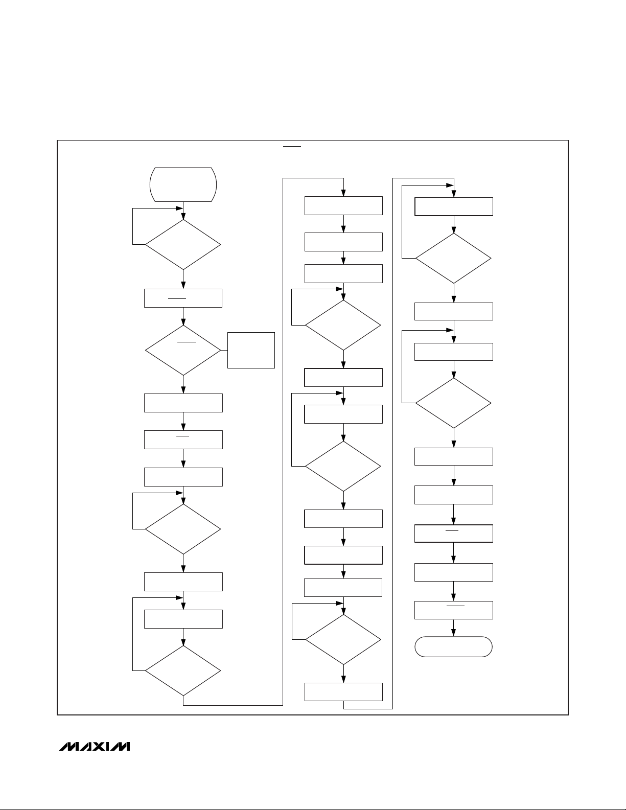
MAX1233/MAX1234
±15kV ESD-Protected Touch-Screen
Controllers Include DAC and Keypad Controller
______________________________________________________________________________________ 37
Figure 22. Touch-Initiated X- , Y-, and Z- Coordinate Screen Scan
YES
ARE THERE
UNREAD SCAN
RESULTS?
PENIRQ LOW
IS PENSTS
START CLOCK
SET BUSY LOW
TURN ON DRIVERS: Y+, Y-
SCREEN
TOUCH
SET
BIT = 1?
NO
YES
GO TO
HOST-INITIATED
SCAN
(FIGURE 24)
PENIRQ-INITIATED
X, Y, AND Z SCREEN SCAN
STORE X- COORDINATES
IN X- REGISTER
POWER DOWN ADC
TURN ON DRIVERS: X+, X-
NO
IS TOUCH-SCREEN
SETTLING DONE?
POWER UP ADC
CONVERT Y- COORDINATES
NO
AVERAGING DONE?
IS DATA
YES
CONVERT Z1- COORDINATES
NO
NO
IS DATA
AVERAGING DONE?
STORE Z1- COORDINATES
- REGISTER
IN Z
1
CONVERT Z2 COORDINATES
IS DATA
AVERAGING DONE?
STORE Z2- COORDINATES
- REGISTER
IN Z
2
YES
YES
NO
IS TOUCH-SCREEN
SETTLING DONE?
YES
POWER UP ADC
CONVERT X- COORDINATES
NO
NO
IS DATA
AVERAGING DONE?
YES
STORE Y- COORDINATES IN
Y- REGISTER
POWER DOWN ADC
TURN ON DRIVERS: Y+, X-
IS TOUCH-SCREEN
SETTLING DONE?
YES
POWER UP ADC
POWER UP ADC
SET BUSY HIGH
TURN OFF CLOCK
RESET PENIRQ HIGH
DONE
Page 38

MAX1233/MAX1234
±15kV ESD-Protected Touch-Screen
Controllers Include DAC and Keypad Controller
38 ______________________________________________________________________________________
Figure 23. Host-Initiated X- and Y- Coordinate Screen Scan
HOST-INITIATED
X- AND Y- SCREEN SCAN
SCREEN
TOUCH
STORE X- COORDINATES
IN X- REGISTER
YES
ARE THERE
UNREAD SCAN
RESULTS?
SET
PENIRQ LOW
IS PENSTS
BIT = 1?
HOST WRITES
ADC CONTROL REGISTER
(PENSTS = ADSTS = 0)
SET BUSY LOW
START CLOCK
TURN ON DRIVERS: Y+, Y-
POWER DOWN ADC
TURN ON DRIVERS: X+, X-
NO
NO
IS TOUCH-SCREEN
SETTLING DONE?
GO TO
YES
TOUCH-INITIATED
SCAN
(FIGURE 21)
NO
CONVERT Y- COORDINATES
NO
STORE Y- COORDINATES IN
YES
POWER UP ADC
IS DATA
AVERAGING DONE?
YES
Y- REGISTER
POWER DOWN ADC
NO
IS TOUCH-SCREEN
SETTLING DONE?
POWER UP ADC
CONVERT X- COORDINATES
NO
IS DATA
AVERAGING DONE?
YES
YES
SET BUSY HIGH
TURN OFF CLOCK
RESET PENIRQ HIGH
DONE
Page 39

MAX1233/MAX1234
±15kV ESD-Protected Touch-Screen
Controllers Include DAC and Keypad Controller
______________________________________________________________________________________ 39
Figure 24. Host-Initiated X-, Y-, and Z- Coordinate Screen Scan
SCREEN
TOUCH
ARE THERE
YES
UNREAD SCAN
RESULTS?
PENIRQ LOW
IS PENSTS
BIT = 1?
HOST WRITES
CONTROL REGISTER
START CLOCK
SET BUSY LOW
TURN ON DRIVERS: Y+, Y-
SET
ADC
HOST-INITIATED
X-, Y-, AND Z- SCREEN SCAN
TURN ON DRIVERS: Y+, X-
NO
IS TOUCH-SCREEN
SETTLING DONE?
TURN ON DRIVERS: X+, X-
NO
NO
IS TOUCH-SCREEN
SETTLING DONE?
GO TO
YES
TOUCH-INITIATED
SCAN
(FIGURE 22)
NO
CONVERT Y- COORDINATES
NO
STORE Y- COORDINATES IN
YES
POWER UP ADC
IS DATA
AVERAGING DONE?
YES
Y- REGISTER
CONVERT Z
NO
STORE Z1- COORDINATES
CONVERT Z2- COORDINATES
NO
YES
POWER UP ADC
- COORDINATES
1
IS DATA
AVERAGING DONE?
YES
- REGISTER
IN Z
1
IS DATA
AVERAGING DONE?
NO
IS TOUCH-SCREEN
SETTLING DONE?
YES
POWER UP ADC
CONVERT X- COORDINATES
NO
IS DATA
AVERAGING DONE?
YES
STORE X- COORDINATES
IN X- REGISTER
POWER DOWN ADC
POWER DOWN ADC
YES
STORE Z2- COORDINATES
- REGISTER
IIN Z
2
POWER DOWN ADC
SET BUSY HIGH
TURN OFF CLOCK
RESET PENIRQ HIGH
DONE
Page 40

MAX1233/MAX1234
±15kV ESD-Protected Touch-Screen
Controllers Include DAC and Keypad Controller
40 ______________________________________________________________________________________
Figure 25. Key-Press-Initiated Debounce Scan
Figure 26. Host-Initiated Debounce Scan
HOST-INITIATED DEBOUNCE SCAN
KEY-PRESS-INITIATED DEBOUNCE SCAN
KEYPAD
TOUCH
YES
ARE THERE
UNREAD DEBOUNCE
RESULTS?
NO
SET
KEYIRQ LOW
NO
IS KEYSTS1 = 1?
YES
START CLOCK
SET BUSY LOW
GO TO HOST-INITIATED
DEBOUNCE SCAN
YES
KEYPAD
TOUCH
ARE THERE
UNREAD DEBOUNCE
RESULTS?
NO
SET
KEYIRQ LOW
IS KEYSTS1 = 1?
NO
HOST WRITES
ADC
CONTROL REGISTER
START CLOCK
YES
GO TO KEY-PRESS-INITIATED
DEBOUNCE SCAN
SET BUSY LOW
SCAN AND DEBOUNCE KEYS
STORE KEYPAD SCAN
RESULTS IN REGISTER
SET BUSY HIGH
RESET KEYIRQ HIGH
DONE
SCAN AND DEBOUNCE KEYS
STORE KEYPAD SCAN
RESULTS IN REGISTER
SET BUSY HIGH
RESET KEYIRQ HIGH
DONE
Page 41

MAX1233/MAX1234
±15kV ESD-Protected Touch-Screen
Controllers Include DAC and Keypad Controller
______________________________________________________________________________________ 41
Equation 5 shows that the maximum output voltage occurs
for the minimum DAC voltage, and that the minimum
output voltage occurs for the maximum DAC voltage.
To ensure that the desired output swing is achieved,
choose appropriate values of R1, R2, and R3.
Calculate V
OUTMAX
using the following equation:
V
OUTMAX
= V
REFMAX
+ (R1
MAX
/ R2
MIN)VREFMAX
+ (R1
MAX
/ R3
MIN
) (V
REFMAX
- V
DACMIN
)
[Equation 6]
If V
OUTMAX
exceeds the maximum ratings of the
LCD/TFT display, the DAC codes that cause the output
voltage to go too high must be avoided.
Calculate V
OUTMIN
using the following equation:
V
OUTMIN
= V
REFMIN
+ (R1
MIN
/ R2
MAX)VREFMIN
+
(R1
MAX
/ R3
MIN
) (V
REFMIN
- V
DACMAX
)
[Equation 7]
If V
OUTMIN
is too low for desired operation, avoid the DAC
codes, which cause the output voltage to go too low.
Connection to Standard Interface
SPI and MICROWIRE Interfaces
When using an SPI interface (Figure 28a) or
MICROWIRE (Figure 28b), set the CPOL = CPHA = 0.
At least four 8-bit operations are necessary to read or
write data to/from the MAX1233/MAX1234. DOUT data
transitions on the serial clock’s falling edge and is
clocked into the µP on the SCLK’s rising edge. The first
Figure 27. LCD Contrast Control Circuit
Figure 28a. SPI Interface
Figure 28b. MICROWIRE Interface
V
BATT
MAX1233
MAX1234
AV
DD
DAC
DACOUT
FEEDBACK
RESISTORS
i
3 R2
R1R3i
SIMPLIFIED DC/DC CONVERTER
1
i
2
ERROR AMP
V
REF
1.25V
MAX1677
CONTROL
V
OUT
(LCD BIAS)
CS
SCK
MISO
SPI
V
DD
SS
MOSI
CS
SCLK
DOUT
DIN
BUSY
PENIRQ
KEYIRQ
MAX1233
MAX1234
CS
SCK
MISO
MICROWIRE
MOSI
CS
SCLK
DOUT
DIN
BUSY
PENIRQ
KEYIRQ
MAX1233
MAX1234
Page 42

MAX1233/MAX1234
±15kV ESD-Protected Touch-Screen
Controllers Include DAC and Keypad Controller
42 ______________________________________________________________________________________
two 8-bit data streams write the command word into the
MAX1233/MAX1234. The next two 8-bit data streams
can contain either the input or output data.
QSPI Interface
Using the high-speed QSPI interface (Figure 29) with
CPOL = 0 and CPHA = 0, the MAX1233/MAX1234 support a maximum f
SCLK
of 10MHz. DOUT data transitions on the serial clock’s falling edge and is clocked
into the µP on the SCLK’s rising edge.
Layout, Grounding, and Bypassing
For best performance, use printed circuit boards with
good layouts; do not use wire-wrap boards even for
prototyping. Ensure that digital and analog signal lines
are separated from each other. Do not run analog and
digital (especially clock) lines parallel to one another, or
digital lines underneath the ADC package.
Figure 30 shows the recommended system ground
connections. Establish a single-point analog ground
(star ground point) at GND. Connect all analog grounds
to the star ground. Connect the digital system ground
to the star ground at this point only. For lowest noise operation, the ground return to the star ground’s power supply
should be low impedance and as short as possible.
High-frequency noise in the power supply may affect
the high-speed comparator in the ADC. Bypass the
supply to the star ground with a 0.1µF capacitor as
close to pins 1 and 2 of the MAX1233/MAX1234 as
possible. Minimize capacitor lead lengths for best supply-noise rejection. If the power supply is very noisy, a
10Ω resistor can be connected as a lowpass filter.
While using the MAX1233/MAX1234 with a resistive
touch screen, the interconnection between the converter and the touch screen should be as short and robust
as possible. Since resistive touch screens have a low
resistance, longer or loose connections are a source of
error. Noise can also be a major source of error in
touch-screen applications (e.g., applications that
require a backlight LCD panel). This EMI noise can be
coupled through the LCD panel to the touch screen
and cause “flickering” of the converted data. Utilizing a
touch screen with a bottom-side metal layer connected
to ground couples the majority of noise to ground. In
addition, the filter capacitors from Y+, Y-, X+, and Xinputs to ground also help reduce the noise further.
Caution should be observed for settling time of the
touch screen.
Definitions
Integral Nonlinearity
Integral nonlinearity (INL) is the deviation of the values
on an actual transfer function from a straight line. This
straight line can be either a best-straight-line fit or a line
drawn between the end points of the transfer function,
once offset and gain errors have been nullified. The
static linearity parameters for the MAX1233/MAX1234
are measured using the end-point method.
Differential Nonlinearity
Differential nonlinearity (DNL) is the difference between
an actual step width and the ideal value of 1LSB. A
DNL error specification of less than 1LSB guarantees
no missing codes and a monotonic transfer function.
Aperture Jitter
Aperture jitter (tAJ) is the sample-to-sample variation in
the time between the samples.
Aperture Delay
Aperture delay (tAD) is the time defined between the
falling edge of the sampling clock and the instant when
an actual sample is taken.
Figure 29. QSPI Interface
Figure 30. Power-Supply Grounding Connection
CS
SCK
MISO
QSPI
V
DD
SS
+3V/+5V +3V/+5VGND
R* = 10Ω
DD
*OPTIONAL
MOSI
SUPPLIES
GNDAV
MAX1233
MAX1234
CS
SCLK
DOUT
MAX1233
MAX1234
DIN
BUSY
PENIRQ
KEYIRQ
DV
DD
DGNDV
DD
DIGITAL
CIRCUITRY
Page 43

MAX1233/MAX1234
±15kV ESD-Protected Touch-Screen
Controllers Include DAC and Keypad Controller
______________________________________________________________________________________ 43
Signal-to-Noise Ratio
For a waveform perfectly reconstructed from digital samples, signal-to-noise ratio (SNR) is the ratio of full-scale
analog input (RMS value) to the RMS quantization error
(residual error). The ideal, theoretical minimum analogto-digital noise is caused by quantization error only and
results directly from the ADC’s resolution (N bits):
SNR = (6.02 ✕ N + 1.76) dB
In reality, there are other noise sources besides quantization noise: thermal noise, reference noise, clock jitter,
etc. SNR is computed by taking the ratio of the RMS
signal to the RMS noise, which includes all spectral
components minus the fundamental, the first five harmonics, and the DC offset.
Signal-to-Noise Plus Distortion
Signal-to-noise plus distortion (SINAD) is the ratio of the
fundamental input frequency’s RMS amplitude to the
RMS equivalent of all other ADC output signals:
SINAD (dB) = 20 ✕ log (Signal
RMS
/ Noise
RMS
)
Effective Number of Bits
Effective number of bits (ENOB) indicates the global
accuracy of an ADC at a specific input frequency and
sampling rate. An ideal ADC’s error consists of
quantization noise only. With an input range equal to
the full-scale range of the ADC, calculate the effective
number of bits as follows:
ENOB = (SINAD - 1.76) / 6.02
Total Harmonic Distortion
Total harmonic distortion (THD) is the ratio of the RMS
sum of the first five harmonics of the input signal to the
fundamental itself. This is expressed as:
where V1is the fundamental amplitude, and V2through
V5are the amplitudes of the 2nd- through 5th-order
harmonics, respectively.
Spurious-Free Dynamic Range
Spurious-free dynamic range (SFDR) is the ratio of RMS
amplitude of the fundamental (maximum signal component) to the RMS value of the next-largest distortion
component.
THD
VVVV
V
=×
+++
⎛
⎝
⎜
⎜
⎞
⎠
⎟
⎟
20
2232425
2
1
2
log
Chip Information
TRANSISTOR COUNT: 28,629
Package Information
For the latest package outline information, go to
www.maxim-ic.com/packages
.
PACKAGE TYPE PACKAGE CODE DOCUMENT NO.
28 QFN G2855-2
21-0091
28 TQFN T2855-6
21-0140
Page 44

MAX1233/MAX1234
±15kV ESD-Protected Touch-Screen
Controllers Include DAC and Keypad Controller
Maxim cannot assume responsibility for use of any circuitry other than circuitry entirely embodied in a Maxim product. No circuit patent licenses are
implied. Maxim reserves the right to change the circuitry and specifications without notice at any time.
44
____________________Maxim Integrated Products, 120 San Gabriel Drive, Sunnyvale, CA 94086 408-737-7600
© 2008 Maxim Integrated Products is a registered trademark of Maxim Integrated Products.
Revision History
REVISION
NUMBER
0 7/02 Initial release —
43/08
REVISION
DATE
DESCRIPTION PAGES CHANGED
Added register address information. Fixed DCLK typo. Fixed CS
timing dependency.
12, 18–27, 29, 41, 42
 Loading...