

For free samples & the latest literature: http://www.maxim-ic.com, or phone 1-800-998-8800.
For small orders, phone 1-800-835-8769.
General Description
The MAX1202/MAX1203 are 12-bit data-acquisition
systems specifically designed for use in applications
with mixed +5V (analog) and +3V (digital) supply voltages. They operate with a single +5V analog supply or
dual ±5V analog supplies, and combine an 8-channel
multiplexer, high-bandwidth track/hold, and serial interface with high conversion speed and low power consumption.
A 4-wire serial interface connects directly to
SPI™/MICROWIRE™ devices without external logic,
and a serial strobe output allows direct connection to
TMS320-family digital signal processors. The
MAX1202/MAX1203 use either the internal clock or an
external serial-interface clock to perform successiveapproximation analog-to-digital conversions. The serial
interface operates at up to 2MHz.
The MAX1202 features an internal 4.096V reference,
while the MAX1203 requires an external reference. Both
parts have a reference-buffer amplifier that simplifies
gain trim. They also have a VL pin that is the power
supply for the digital outputs. Output logic levels (3V,
3.3V, or 5V) are determined by the value of the voltage
applied to this pin.
These devices provide a hard-wired SHDN pin and two
software-selectable power-down modes. Accessing the
serial interface automatically powers up the devices. A
quick turn-on time enables the MAX1202/MAX1203 to
be shut down between conversions, allowing the user
to optimize supply currents. By customizing powerdown between conversions, supply current can drop
below 10µA at reduced sampling rates.
The MAX1202/MAX1203 are available in 20-pin SSOP
and DIP packages, and are specified for the commercial, extended, and military temperature ranges.
Applications
5V/3V Mixed-Supply Systems
Data Acquisition
High-Accuracy Process Control
Battery-Powered Instruments
Medical Instruments
Features
♦ 8-Channel Single-Ended or 4-Channel
Differential Inputs
♦ Operates from Single +5V or Dual ±5V Supplies
♦ User-Adjustable Output Logic Levels
(2.7V to 5.25V)
♦ Low Power: 1.5mA (operating mode)
2µA (power-down mode)
♦ Internal Track/Hold, 133kHz Sampling Rate
♦ Internal 4.096V Reference (MAX1202)
♦ SPI/MICROWIRE/TMS320-Compatible
4-Wire Serial Interface
♦ Software-Configurable Unipolar/Bipolar Inputs
♦ 20-Pin DIP/SSOP
MAX1202/MAX1203
5V, 8-Channel, Serial, 12-Bit ADCs
with 3V Digital Interface
________________________________________________________________
Maxim Integrated Products
1
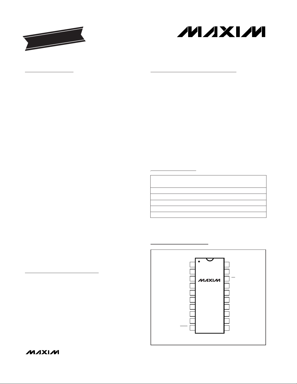
20
19
18
17
16
15
14
13
12
11
1
2
3
4
5
6
7
8
9
10
TOP VIEW
DIP/SSOP
V
DD
SCLK
CS
DIN
SSTRB
DOUT
VL
GND
REFADJ
REF
SHDN
V
SS
CH7
CH6
CH5
CH4
CH3
CH2
CH1
CH0
MAX1202
MAX1203
Pin Configuration
19-1173; Rev 2; 5/98
EVALUATION KIT
AVAILABLE
Typical Operating Circuit appears at end of data sheet.
SPI is a registered trademark of Motorola, Inc.
MICROWIRE is a registered trademark of National
Semiconductor Corp.
Ordering Information continued at end of data sheet.
*
Dice are specified at TA= +25°C, DC parameters only.
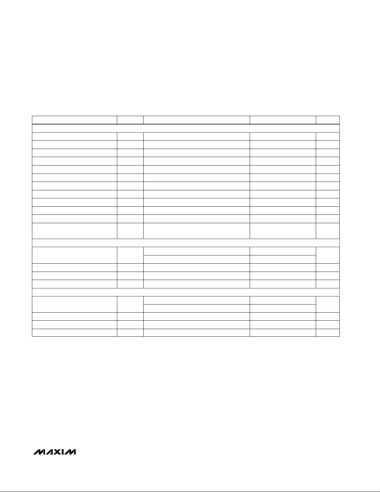
±1Dice*0°C to +70°CMAX1202BC/D
MAX1202BCAP
MAX1202ACAP
MAX1202BCPP
MAX1202ACPP
PART TEMP. RANGE
0°C to +70°C
0°C to +70°C
0°C to +70°C
0°C to +70°C 20 SSOP
20 SSOP
20 Plastic DIP
20 Plastic DIP
PIN-PACKAGE
INL
(LSB)
±1/2
±1
±1/2
±1
Ordering Information
MAX1202/MAX1203
5V, 8-Channel, Serial, 12-Bit ADCs
with 3V Digital Interface
2 _______________________________________________________________________________________
ABSOLUTE MAXIMUM RATINGS
Stresses beyond those listed under “Absolute Maximum Ratings” may cause permanent damage to the device. These are stress ratings only, and functional
operation of the device at these or any other conditions beyond those indicated in the operational sections of the specifications is not implied. Exposure to
absolute maximum rating conditions for extended periods may affect device reliability.
VDDto GND ................................................................-0.3V to 6V
VL ...............................................................-0.3V to (V
DD
+ 0.3V)
V
SS
to GND.................................................................0.3V to -6V
V
DD
to VSS................................................................-0.3V to 12V
CH0–CH7 to GND............................(V
SS
- 0.3V) to (VDD+ 0.3V)
CH0–CH7 Total Input Current...........................................±20mA
REF to GND................................................-0.3V to (V
DD
+ 0.3V)
REFADJ to GND.........................................-0.3V to (V
DD
+ 0.3V)
Digital Inputs to GND .................................-0.3V to (V
DD
+ 0.3V)
Digital Outputs to GND.................................-0.3V to (VL + 0.3V)
Digital Output Sink Current.................................................25mA
Continuous Power Dissipation (T
A
= +70°C)
Plastic DIP (derate 11.11mW/°C above +70°C) ...........889mW
SSOP (derate 8.00mW/°C above +70°C) .....................640mW
CERDIP (derate 11.11mW°C above +70°C).................889mW
Operating Temperature Ranges
MAX1202_C_P/MAX1203_C_P............................0°C to +70°C
MAX1202_E_P/MAX1203_E_P..........................-40°C to +85°C
MAX1202BMJP/MAX1203BMJP.....................-55°C to +125°C
Storage Temperature Range.............................-60°C to +150°C
Lead Temperature (soldering, 10sec).............................+300°C
ELECTRICAL CHARACTERISTICS
(VDD= +5V ±5%, VL = 2.7V to 3.6V; VSS= 0V or -5V ±5%; f
SCLK
= 2.0MHz, external clock (50% duty cycle); 15 clocks/conversion
cycle (133ksps); MAX1202—4.7µF capacitor at REF pin; MAX1203—external reference, V
REF
= 4.096V applied to REF pin;
T
A
= T
MIN
to T
MAX
; unless otherwise noted.)
-3dB rolloff MHz4.5
MAX1202A/MAX1203A
Small-Signal Bandwidth
kHz800
VIN= 4.096Vp-p, 65kHz (Note 4)
External reference, 4.096V
MAX1202B/MAX1203B
No missing codes over temperature
CONDITIONS
Full-Power Bandwidth
±3MAX1202 (all grades)
dB-85Channel-to-Channel Crosstalk
dB80SFDRSpurious-Free Dynamic Range
dB-80THD
Total Harmonic Distortion
(up to the 5th harmonic)
dB70SINADSignal-to-Noise + Distortion Ratio
LSB
±0.5
INLRelative Accuracy (Note 2)
Bits12Resolution
LSB±0.1
Channel-to-Channel
Offset Matching
ppm/°C±0.8Gain Temperature Coefficient
±1.0
LSB±1.0DNLDifferential Nonlinearity
UNITSMIN TYP MAXSYMBOLPARAMETER
LSB±3.0Offset Error
±1.5 LSB
±3
Gain Error (Note 3)
External reference, 4.096V
MAX1203A
MAX1203B
DC ACCURACY (Note 1)
DYNAMIC SPECIFICATIONS (10kHz sine-wave input, 4.096Vp-p, 133ksps, 2.0MHz external clock, bipolar-input mode)
MAX1202/MAX1203
5V, 8-Channel, Serial, 12-Bit ADCs
with 3V Digital Interface
_______________________________________________________________________________________ 3
ELECTRICAL CHARACTERISTICS (continued)
(VDD= +5V ±5%, VL = 2.7V to 3.6V; VSS= 0V or -5V ±5%; f
SCLK
= 2.0MHz, external clock (50% duty cycle); 15 clocks/conversion
cycle (133ksps); MAX1202—4.7µF capacitor at REF pin; MAX1203—external reference, V
REF
= 4.096V applied to REF pin;
T
A
= T
MIN
to T
MAX
; unless otherwise noted.)
MAX1202AC
TA= +25°C
External clock, 2MHz, 12 clocks/conversion
(Note 6)
On/off leakage current, V
CH_
= ±5V
Bipolar, VSS= -5V
Unipolar, VSS= 0V
6
Used for data transfer only
Internal compensation mode (Note 6)
Internal clock
MAX1202AE
External compensation mode
External compensation mode, 4.7µF
±30 ±60
CONDITIONS
ppm/°C
±30 ±50
V
REF
Temperature Coefficient
mA30REF Short-Circuit Current
V4.076 4.096 4.116REF Output Voltage
pF16Input Capacitance
µA±0.01 ±1Multiplexer Leakage Current
±V
REF
/2
4.7
V
V
REF
Input Voltage Range, SingleEnded and Differential (Note 7)
0 2.0
±30
0.1 0.4
MAX1202B
µF
MHz
0.1 2.0
External Clock Frequency Range
MHz1.7Internal Clock Frequency
0.01
0mA to 0.5mA output load mV2.5Load Regulation (Note 8)
ns10Aperture Delay
µs1.5t
ACQ
Track/Hold Acquisition Time
µs
5.5 10
t
CONV
Conversion Time (Note 5)
Internal compensation mode
µF
0
Capacitive Bypass at REF
Capacitive Bypass at REFADJ
UNITSMIN TYP MAXSYMBOLPARAMETER
ps
%±1.5REFADJ Adjustment Range
V
2.50 VDD+
50mV
Input Voltage Range
µA200 350Input Current
kΩ
12 20Input Resistance
SHDN = 0V
µA1.5 10REF Input Current in Shutdown
V
VDD50mV
REFADJ Buffer Disable Threshold
<50Aperture Jitter
CONVERSION RATE
INTERNAL REFERENCE (MAX1202 only, reference-buffer enabled)
ANALOG INPUT
EXTERNAL REFERENCE AT REF (Reference buffer disabled, V
REF
= 4.096V)
µA
MAX1202/MAX1203
5V, 8-Channel, Serial, 12-Bit ADCs
with 3V Digital Interface
4 _______________________________________________________________________________________
ELECTRICAL CHARACTERISTICS (continued)
(VDD= +5V ±5%, VL = 2.7V to 3.6V; VSS= 0V or -5V ±5%; f
SCLK
= 2.0MHz, external clock (50% duty cycle); 15 clocks/conversion
cycle (133ksps); MAX1202—4.7µF capacitor at REF pin; MAX1203—external reference, V
REF
= 4.096V applied to REF pin;
T
A
= T
MIN
to T
MAX
; unless otherwise noted.)
Operating mode mA1.5 2.5
Internal compensation mode
VDD= 5V ±5%; external reference, 4.096V;
full-scale input
mV±0.06 ±0.5
V
Fast power-down (Note 9) 30 70
External compensation mode
MAX1202
MAX1202
CONDITIONS
2.70 5.25VLLogic Supply Voltage
VL = VDD= 5V µA10I
VL
Logic Supply Current (Notes 6, 10)
PSR
Positive Supply Rejection
(Note 11)
VSS= -5V ±5%; external reference, 4.096V;
full-scale input
mV±0.01 ±0.5PSR
Negative Supply Rejection
(Note 11)
External reference, 4.096V; full-scale input mV±0.06 ±0.5PSR
Logic Supply Rejection
(Note 12)
µA
µF
0
Capacitive Bypass at REF
V0 or -5 ±5%V
SS
Negative Supply Voltage
V5 ±5%V
DD
Positive Supply Voltage
4.7
1.68
±50
UNITSMIN TYP MAXSYMBOLPARAMETER
MAX1203
V/V
1.64
Reference-Buffer Gain
MAX1203
µA
±5
REFADJ Input Current
Full power-down 10
Operating mode and fast power-down
µA
50
I
SS
Negative Supply Current
Full power-down (Note 9)
µA
I
DD
210
Positive Supply Current
EXTERNAL REFERENCE AT REFADJ
POWER REQUIREMENTS
MAX1202/MAX1203
5V, 8-Channel, Serial, 12-Bit ADCs
with 3V Digital Interface
_______________________________________________________________________________________ 5
ELECTRICAL CHARACTERISTICS (continued)
(VDD= +5V ±5%, VL = 2.7V to 3.6V; VSS= 0V or -5V ±5%; f
SCLK
= 2.0MHz, external clock (50% duty cycle); 15 clocks/conversion
cycle (133ksps); MAX1202—4.7µF capacitor at REF pin; MAX1203—external reference, V
REF
= 4.096V applied to REF pin;
T
A
= T
MIN
to
T
MAX
; unless otherwise noted.)
CS = VL (Note 6)
CS = VL
I
SOURCE
= 1mA
I
SINK
= 3mA
SHDN = open
SHDN = 0V
SHDN = V
DD
(Note 6)
VIN= 0V or V
DD
SHDN = open
I
SINK
= 5mA
CONDITIONS
pF15C
OUT
Three-State Output Capacitance
µA±10I
L
Three-State Leakage Current
VVL - 0.5V
OH
Output Voltage High
V
0.4
V
OL
Output Voltage Low
nA-100 100
SHDN Maximum Allowed
Leakage, Mid-Input
V2.75V
FLT
SHDN Voltage, Floating
µA-4.0I
SL
SHDN Input Current, Low
µA4.0I
SH
SHDN Input Current, High
VV
DD
- 0.5V
SH
SHDN Input High Voltage
V
0.4
V
OL
Output Voltage Low
V0.8V
IL
V2.0V
IH
DIN, SCLK, CS Input High Voltage
DIN, SCLK, CS Input Low Voltage
I
SINK
= 8mA 0.3
V1.5 VDD- 1.5
I
SINK
= 6mA
V
SM
0.3
pF15C
IN
DIN, SCLK, CS Input Capacitance
µA±1I
IN
DIN, SCLK, CS Input Leakage
SHDN Input Mid-Voltage
I
SOURCE
= 1mA V
V0.15V
HYST
DIN, SCLK, CS Input Hysteresis
4V
OH
Output Voltage High
CS = 5V
µA±10I
L
Three-State Leakage Current
UNITSMIN TYP MAXSYMBOLPARAMETER
CS = 5V (Note 6)
pF15C
OUT
Three-State Output Capacitance
V0.5V
SL
SHDN Input Low Voltage
DIGITAL INPUTS: DIN, SCLK,
CCSS, SSHHDDNN
DIGITAL OUTPUTS: DOUT, SSTRB (VL = 2.7V to 3.6V)
DIGITAL OUTPUTS: DOUT, SSTRB (VL = 4.75V to 5.25V)
MAX1202/MAX1203
5V, 8-Channel, Serial, 12-Bit ADCs
with 3V Digital Interface
6 _______________________________________________________________________________________
TIMING CHARACTERISTICS
(VDD= +5V ±5%, VL = 2.7V to 3.6V, VSS= 0V or -5V ±5%, TA= T
MIN
to T
MAX
, unless otherwise noted.)
Note 1: Tested at V
DD
= 5.0V; VSS= 0V; unipolar-input mode.
Note 2: Relative accuracy is the analog value’s deviation (at any code) from its theoretical value after the full-scale range is calibrated.
Note 3: MAX1202—internal reference, offset nulled; MAX1203—external reference (V
REF
= 4.096V), offset nulled.
Note 4: On-channel grounded; sine wave applied to all off-channels.
Note 5: Conversion time is defined as the number of clock cycles multiplied by the clock period; clock has 50% duty cycle.
Note 6: Guaranteed by design. Not subject to production testing.
Note 7: Common-mode range for analog inputs is from V
SS
to VDD.
Note 8: External load should not change during the conversion for specified accuracy.
Note 9: Shutdown supply current is measured with VL at 3.3V, and with all digital inputs tied to either VL or GND;
REFADJ = GND. Shutdown supply current is also dependent on V
IH
(Figure 12c).
Note 10: Logic supply current is measured with the digital outputs (DOUT and SSTRB) disabled (CS high). When the outputs are
active (CS low), the logic supply current depends on f
SCLK
, and on the static and capacitive load at DOUT and SSTRB.
Note 11: Measured at V
SUPPLY
+ 5% and V
SUPPLY
- 5% only.
Note 12: Measured at VL = 2.7V and VL = 3.6V.
ns100t
CSS
External-clock mode only, C
LOAD
= 100pF ns
CS to SCLK Rise Setup
240
C
LOAD
= 100pF ns
ns20 240
ns0
t
DO
SCLK Fall to Output Data Valid
t
CSH
CONDITIONS
CS to SCLK Rise Hold
240t
DV
CS Fall to Output Enable
C
LOAD
= 100pF ns240t
TR
CS Rise to Output Disable
t
SDV
CS Fall to SSTRB Output Enable
(Note 6)
External-clock mode only, C
LOAD
= 100pF ns240t
STR
CS Rise to SSTRB Output
Disable (Note 6)
Internal-clock mode only ns0t
SCK
SSTRB Rise to SCLK Rise
(Note 6)
ns200t
CH
SCLK Pulse Width High
ns200t
CL
SCLK Pulse Width Low
C
LOAD
= 100pF ns240t
SSTRB
SCLK Fall to SSTRB
C
LOAD
= 100pF
ns0t
DH
DIN to SCLK Hold
µs1.5t
ACQ
Acquisition Time
ns100t
DS
DIN to SCLK Setup
UNITSMIN TYP MAXSYMBOLPARAMETER
MAX1202/MAX1203
5V, 8-Channel, Serial, 12-Bit ADCs
with 3V Digital Interface
_______________________________________________________________________________________
7
1.0
2.0
1.8
1.6
1.4
1.2
4.5
SUPPLY CURRENT
vs. SUPPLY VOLTAGE
MAX1202 TOC01
SUPPLY VOLTAGE (V)
SUPPLY CURRENT (mA)
5.34.7 5.1 5.54.9
MAX1202
MAX1203
0
-60
SUPPLY CURRENT
vs. TEMPERATURE
0.5
MAX1202 TOC02
TEMPERATURE (°C)
SUPPLY CURRENT (mA)
100
2.0
1.0
1.5
-20 60 140
3.0
2.5
20
MAX1202
MAX1203
6
5
0
-60
SHUTDOWN SUPPLY CURRENT
vs. TEMPERATURE
4
MAX1202 TOC03
TEMPERATURE (°C)
SHUTDOWN SUPPLY CURRENT (µA)
60
2
1
-20 20
3
100
140
REFADJ = GND
FULL POWER-DOWN
0.8
0.6
0.7
0.5
0
-60
INTEGRAL NONLINEARITY
vs. TEMPERATURE
0.4
MAX1202 TOC04
TEMPERATURE (°C)
INL (LSB)
60
0.2
0.1
-20 20
0.3
100
140
3
2
-3
-60
CHANNEL-TO-CHANNEL OFFSET-ERROR
MATCHING vs. TEMPERATURE
1
MAX1202 TOC07
TEMPERATURE (°C)
OFFSET-ERROR MATCHING (LSB)
60
-1
-2
-20 20
0
100
140
2.0
1.0
1.5
0.5
-2.0
-60
OFFSET ERROR
vs. TEMPERATURE
0
MAX1202 TOC05
TEMPERATURE (°C)
OFFSET ERROR (LSB)
60
-1.0
-1.5
-20 20
-0.5
100
140
5
3
4
1
2
0
-5
-60
GAIN ERROR
vs. TEMPERATURE
-1
MAX1202 TOC06
TEMPERATURE (°C)
GAIN ERROR (LSB)
60
-3
-4
-20 20
-2
100
140
DIFFERENTIAL
SINGLE-ENDED
5
3
4
1
2
0
-5
-60
CHANNEL-TO-CHANNEL GAIN-ERROR
MATCHING vs. TEMPERATURE
-1
MAX1202 TOC08
TEMPERATURE (°C)
GAIN-ERROR MATCHING (LSB)
60
-3
-4
-20 20
-2
100
140
__________________________________________Typical Operating Characteristics
(VDD= 5V ±5%; VL = 2.7V to 3.6V; VSS= 0V; f
SCLK
= 2.0MHz, external clock (50% duty cycle); 15 clocks/conversion cycle
(133ksps); MAX1202—4.7µF capacitor at REF pin; MAX1203—external reference, V
REF
= 4.096V applied to REF pin; TA = +25°C;
unless otherwise noted.)
______________________________________________________________Pin Description
MAX1202/MAX1203
5V, 8-Channel, Serial, 12-Bit ADCs
with 3V Digital Interface
8 _______________________________________________________________________________________
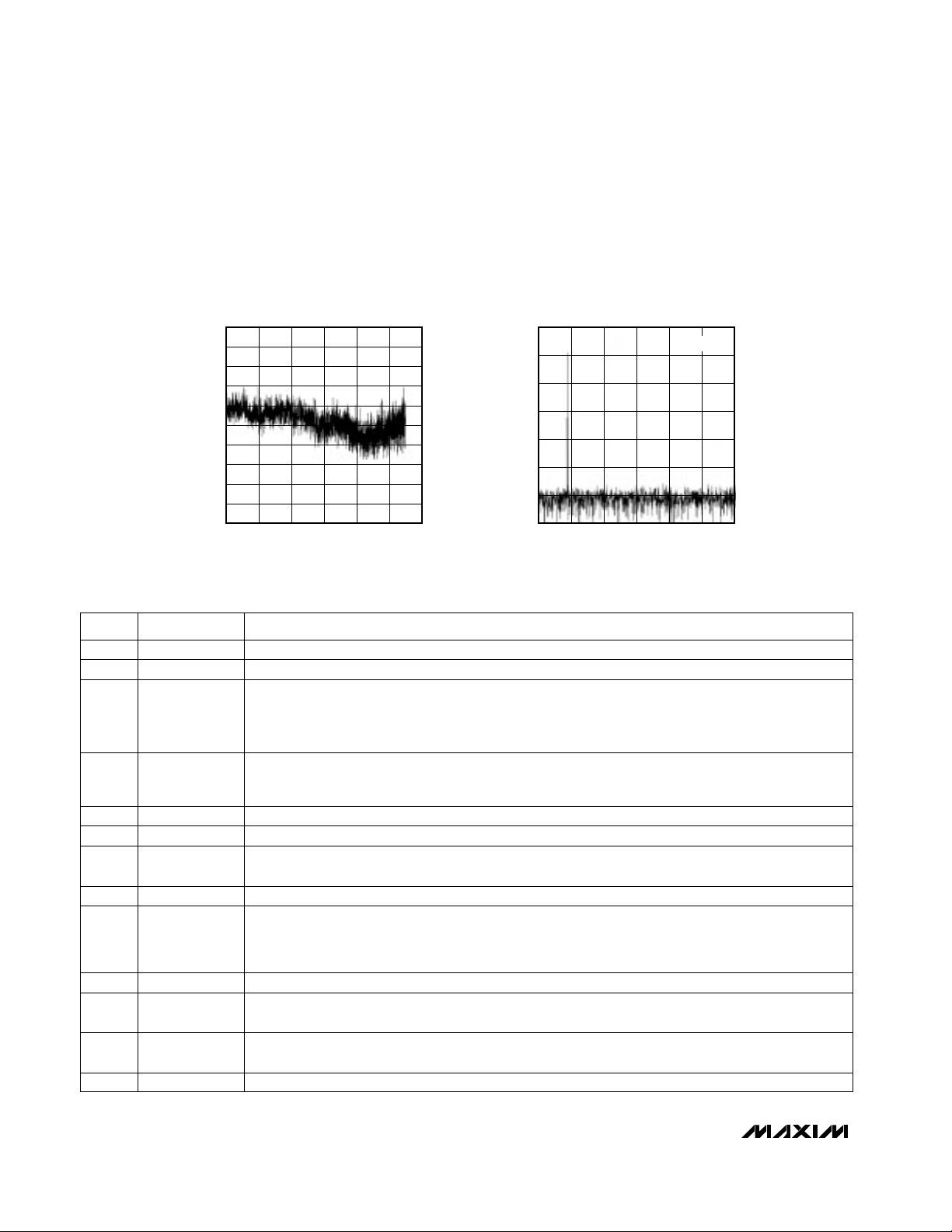
-1.0
-0.8
-0.6
-0.4
0
INTEGRAL NONLINEARITY
vs. DIGITAL
1.0
0.4
0.6
0.8
MAX1202 TOC09
DIGITAL CODE
INL (LSB)
3000
0
-0.2
750 1500 2250
0.2
3750
4500
-120
0
FFT PLOT
20
MAX1202 TOC10
FREQUENCY (kHz)
AMPLITUDE (dB)
-20
-40
-60
-80
-100
33.25
0
66.50
VSS = -5V
____________________________Typical Operating Characteristics (continued)
(VDD= 5V ±5%; VL = 2.7V to 3.6V; VSS= 0V; f
SCLK
= 2.0MHz, external clock (50% duty cycle); 15 clocks/conversion cycle
(133ksps); MAX1202—4.7µF capacitor at REF pin; MAX1203—external reference, V
REF
= 4.096V applied to REF pin; TA = +25°C;
unless otherwise noted.)
Serial-Strobe Output. In internal clock mode, SSTRB goes low when the MAX1202/MAX1203 begin
the analog-to-digital conversion, and goes high when the conversion is finished. In external clock
mode, SSTRB pulses high for one clock period before the MSB decision. High impedance when CS
is high (external clock mode).
SSTRB16
Serial-Data Input. Data is clocked in at SCLK’s rising edge.DIN17
Active-Low Chip Select. Data is not clocked into DIN unless CS is low. When CS is high, DOUT is
high impedance.
CS
18
Serial-Clock Input. SCLK clocks data in and out of the serial interface. In external clock mode, SCLK
also sets the conversion speed. (Duty cycle must be 40% to 60% in external clock mode.)
SCLK19
Positive Supply Voltage, +5V ±5%V
DD
20
Input to the Reference-Buffer Amplifier. Tie REFADJ to V
DD
to disable the reference-buffer amplifier.REFADJ12
Ground; IN- Input for Single-Ended ConversionsGND13
Supply Voltage for Digital Output Pins. Voltage applied to VL determines the positive output swing of
the Digital Outputs (DOUT, SSTRB). 2.7V ≤ VL ≤ 5.25V.
VL14
Serial-Data Output. Data is clocked out at SCLK’s falling edge. High impedance when CS is high.
DOUT15
Reference-Buffer Output/ADC Reference Input. In internal reference mode (MAX1202 only), the reference buffer provides a 4.096V nominal output, externally adjustable at REFADJ. In external reference
mode, disable the internal buffer by pulling REFADJ to V
DD.
REF11
Three-Level Shutdown Input. Pulling SHDN low shuts the MAX1202/MAX1203 down to 10µA (max)
supply current; otherwise, the MAX1202/MAX1203 are fully operational. Pulling SHDN to V
DD
puts the
reference-buffer amplifier in internal compensation mode. Letting SHDN float puts the referencebuffer amplifier in external compensation mode.
SHDN
10
PIN
Negative Supply Voltage. Tie VSSto -5V ±5% or to GND.V
SS
9
Sampling Analog InputsCH0–CH71–8
FUNCTIONNAME

MAX1202/MAX1203
5V, 8-Channel, Serial, 12-Bit ADCs
with 3V Digital Interface
_______________________________________________________________________________________ 9
_______________Detailed Description
The MAX1202/MAX1203 analog-to-digital converters
(ADCs) use a successive-approximation conversion
technique and input track/hold (T/H) circuitry to convert
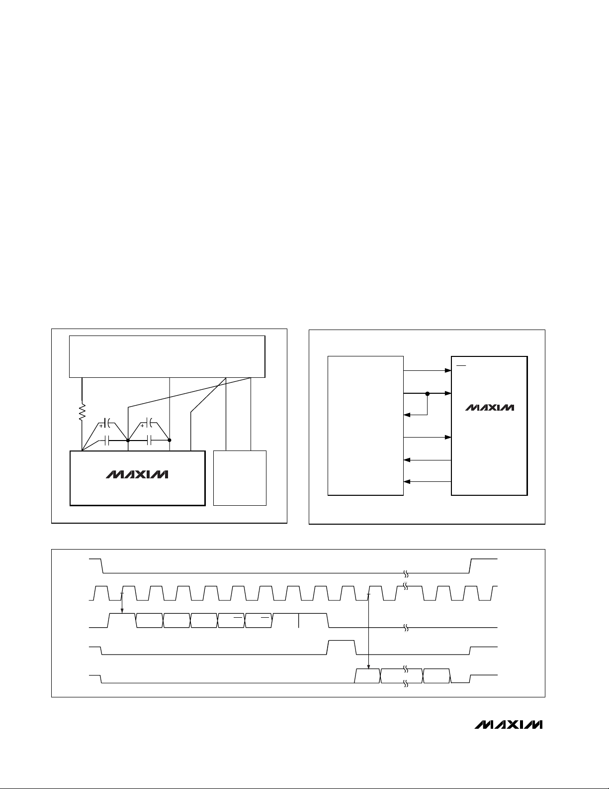
an analog signal to a 12-bit digital output. A flexible serial interface provides easy interface to 3V microprocessors (µPs). Figure 3 is the MAX1202/MAX1203 block
diagram.
Pseudo-Differential Input
Figure 4 shows the ADC’s analog comparator’s sampling architecture. In single-ended mode, IN+ is internally switched to CH0–CH7 and IN- is switched to
GND. In differential mode, IN+ and IN- are selected
from pairs of CH0/CH1, CH2/CH3, CH4/CH5, and
CH6/CH7. Configure the channels using Tables 3
and 4.
In differential mode, IN- and IN+ are internally switched
to either of the analog inputs. This configuration is
pseudo-differential such that only the signal at IN+ is
sampled. The return side (IN-) must remain stable (typically within ±0.5LSB, within ±0.1LSB for best results)
with respect to GND during a conversion. To do this,
connect a 0.1µF capacitor from IN- (of the selected
analog input) to GND.
During the acquisition interval, the channel selected as
the positive input (IN+) charges capacitor C
HOLD
. The
acquisition interval spans three SCLK cycles and ends
on the falling SCLK edge after the input control word’s
last bit is entered. The T/H switch opens at the end of
the acquisition interval, retaining charge on C
HOLD
as a
sample of the signal at IN+.
The conversion interval begins with the input multiplex-
er switching C
HOLD
from the positive input (IN+) to the
negative input (IN-). In single-ended mode, IN- is simply GND. This unbalances node ZERO at the comparator’s input. The capacitive DAC adjusts during the
remainder of the conversion cycle to restore node
ZERO to 0V within the limits of 12-bit resolution.
This action is equivalent to transferring a charge of
16pF x [(VIN+) - (VIN-)] from C
HOLD
to the binaryweighted capacitive DAC, which in turn forms a digital
representation of the analog input signal.
Figure 1. Load Circuits for Enable Time
Figure 2. Load Circuits for Disable Time
Figure 3. Block Diagram
+3.3V
3k
C
LOAD
GND
DOUT
C
LOAD
GND
3k
DOUT
a. High-Z to V
OH
and VOL to V
OH
b. High-Z to VOL and VOH to V
OL
DOUT
3k
GND
C
LOAD
18
CS
19
SCLK
DOUT
+3.3V
3k
C
GND
LOAD
DIN
SHDN
CH0
CH1
CH2
CH3
CH4
CH5
CH6
CH7
GND
REFADJ
REF
INPUT
17
SHIFT
REGISTER
10
1
2
3
4
ANALOG
INPUT
5
MUX
6
7
8
13
REFERENCE
(MAX1202)
12
11
+2.44V
CONTROL
LOGIC
T/H
MAX1202
MAX1203
20k
CLOCK
IN
A
≈ 1.68
+4.096V
INT
CLOCK
12-BIT
SAR
ADC
REF
OUTPUT
SHIFT
REGISTER
OUT
15
DOUT
16
SSTRB
20
V
DD
14
VL
9
V
SS
to High-Z b. VOL to High-Z
a. V
OH

MAX1202/MAX1203
5V, 8-Channel, Serial, 12-Bit ADCs
with 3V Digital Interface
10 ______________________________________________________________________________________
Track/Hold
The T/H enters tracking mode on the falling clock edge
after the fifth bit of the 8-bit control word is shifted in. The
T/H enters hold mode on the falling clock edge after the
eighth bit of the control word is shifted in. IN- is connected to GND if the converter is set up for single-ended
inputs, and the converter samples the “+” input. IN- connects to the “-” input if the converter is set up for differential inputs, and the difference of |N+ - IN- is sampled.
The positive input connects back to IN+, at the end of
the conversion, and C
HOLD
charges to the input signal.
The time required for the T/H to acquire an input signal
is a function of how quickly its input capacitance is
charged. If the input signal’s source impedance is high,
acquisition time increases and more time must be
allowed between conversions. The acquisition time,
t
ACQ
, is the maximum time the device takes to acquire
the signal, and is also the minimum time needed for the
signal to be acquired. It is calculated by the following:
t
ACQ
= 9 x (RS+ RIN) x 16pF
where R
IN
= 9kΩ, RS= the source impedance of the
input signal, and t
ACQ
is never less than 1.5µs. Source
impedances below 1kΩ do not significantly affect the
ADC’s AC performance. Higher source impedances can
be used if an input capacitor is connected to the analog
inputs, as shown in Figure 5. Note that the input capacitor forms an RC filter with the input source impedance,
limiting the ADC’s signal bandwidth.
Figure 5. Quick-Look Circuit
CH0
CH1
CH2
CH3
CH4
CH5
CH6
CH7
GND
C
SWITCH
TRACK
T/H
SWITCH
9k
R
IN
C
HOLD
HOLD
12-BIT CAPACITIVE DAC
REF
ZERO
COMPARATOR
–
+
16pF
SINGLE-ENDED MODE: IN+ = CHO–CH7, IN- = GND.
DIFFERENTIAL MODE:
AT THE SAMPLING INSTANT,
THE MUX INPUT SWITCHES
FROM THE SELECTED IN+
CHANNEL TO THE SELECTED
IN- CHANNEL.
INPUT
MUX
IN+ AND IN- SELECTED FROM PAIRS OF
CH0/CH1, CH2/CH3, CH4/CH5, CH6/CH7.
Figure 4. Equivalent Input Circuit
+3V
0.1µF
0V TO
4.096V
ANALOG
0.01µF
INPUT
C2
0.01µF
*FULL-SCALE ANALOG INPUT, CONVERSION RESULT = $FFF (HEX).
**REQUIRED FOR MAX1203 ONLY.
C1
4.7µF
VL
MAX1202
MAX1203
CH7
REFADJ
REF
+2.5V
+2.5V
REFERENCE
SCLK
SSTRB
DOUT
SHDN
**
V
GND
V
DIN
DD
0.1µF
SS
CS
+3V
N.C.
+5V
4.7µF
2MHz
OSCILLATOR
CH1 CH2
OSCILLOSCOPE
CH3
SCLK
SSTRB
DOUT*
CH4

Table 1a. Unipolar Full Scale and Zero
Scale
MAX1202/MAX1203
5V, 8-Channel, Serial, 12-Bit ADCs
with 3V Digital Interface
______________________________________________________________________________________ 11
Input Bandwidth
The ADC’s input tracking circuitry has a 4.5MHz
small-signal bandwidth. Therefore it is possible to digitize high-speed transient events and measure periodic
signals with bandwidths exceeding the ADC’s sampling
rate by using undersampling techniques. To avoid
high-frequency signals being aliased into the frequency
band of interest, anti-alias filtering is recommended.
Analog Input Range and Input Protection
Internal protection diodes, which clamp the analog
inputs to VDDand VSS, allow the analog input pins to
swing from (VSS- 0.3V) to (VDD+ 0.3V) without damage. However, for accurate conversions near full scale,
the inputs must not exceed VDDby more than 50mV, or
be lower than VSSby 50mV.
If the analog input exceeds 50mV beyond the supplies, do not forward bias the protection diodes of
off-channels more than 2mA.
The full-scale input voltage depends on the voltage at
REF (Tables 1a and 1b).
Quick Look
Use the circuit of Figure 5 to quickly evaluate the
MAX1202/MAX1203’s analog performance. The
MAX1202/MAX1203 require a control byte to be written
to DIN before each conversion. Tying DIN to +3V feeds
in control byte $FF hex, which triggers single-ended
unipolar conversions on CH7 in external clock mode
without powering down between conversions. In external clock mode, the SSTRB output pulses high for one
clock period before the most significant bit of the 12-bit
conversion result shifts out of DOUT. Varying the analog input to CH7 alters the sequence of bits from
DOUT. A total of 15 clock cycles per conversion is
required. All SSTRB and DOUT output transitions occur
on SCLK’s falling edge.
How to Start a Conversion
Clocking a control byte into DIN starts conversion on
the MAX1202/MAX1203. With CS low, each rising edge
on SCLK clocks a bit from DIN into the MAX1202/
MAX1203’s internal shift register. After CS falls, the first
logic “1” bit defines the control byte’s MSB. Until this
first “start” bit arrives, any number of logic “0” bits can
be clocked into DIN with no effect. Table 2 shows the
control-byte format.
The MAX1202/MAX1203 are fully compatible with
SPI/MICROWIRE devices. For SPI, select the correct
clock polarity and sampling edge in the SPI control registers: set CPOL = 0 and CPHA = 0. MICROWIRE and
SPI both transmit and receive a byte at the same time.
Using the
Typical Operating Circuit
, the simplest software interface requires only three 8-bit transfers to perform a conversion (one 8-bit transfer to configure the
ADC, and two more 8-bit transfers to clock out the
12-bit conversion result).
Table 1b. Bipolar Full Scale, Zero Scale,
and Negative Full Scale
REFERENCE
External
ZERO
SCALE
0V
0V
at REFADJ
at REF
FULL SCALE
V
REFADJ
x A*
V
REF
0VInternal +4.096V
-1/2 V
REFADJ
x A*
-1/2 V
REF
NEGATIVE
FULL SCALE
-4.096V / 2
+1/2 V
REF
+1/2 V
REFADJ
x A*
0V
0V
+4.096V / 2
FULL SCALE
0V
ZERO
SCALE
at
REFADJ
External
REFERENCE
Internal
at REF
*
A = 1.68 for the MAX1202, 1.64 for the MAX1203.
*
A = 1.68 for the MAX1202, 1.64 for the MAX1203.

MAX1202/MAX1203
5V, 8-Channel, Serial, 12-Bit ADCs
with 3V Digital Interface
12 ______________________________________________________________________________________
Table 2. Control-Byte Format
Table 3. Channel Selection in Single-Ended Mode (SGL/
DDIIFF
= 1)
SEL1 SEL0
0 0 0
CH4 CH5SEL2 CH6 CH7 GND
–
1 0 0
–+
0 0 1
–+
1 0
CH0
+
1
–+
0 1
CH1
0
+ –
1 1
CH3
0
+ –
0 1
CH2
1
+ –
1 1 1
+ –
Table 4. Channel Selection in Differential Mode (SGL/
DDIIFF
= 0)
SEL1 SEL0
0 0 0
CH4 CH5SEL2 CH6 CH7
0 0 1
–+
0 1 0
+ –
0 1
CH0
+
1
+ –
1 0
CH1
–
0
– +
1 0
CH3
1
+–
1 1
CH2
0
– +
1 1 1
– +
PD0
Bit 0
(LSB)
SGL/DIF
Bit 2
PD1
Bit 1
UNI/BIP
Bit 3
SEL 0
Bit 4
Bit 7
(MSB)
SEL 1SEL 2START
Bit 5Bit 6
1 = unipolar, 0 = bipolar. Selects unipolar or bipolar conversion mode. In unipolar mode, an
analog input signal from 0V to V
REF
can be converted; in bipolar mode, the signal can range
from -V
REF
/ 2 to +V
REF
/ 2.
1 = single ended, 0 = differential. Selects single-ended or differential conversions. In singleended mode, input signal voltages are referred to GND. In differential mode, the voltage difference between two channels is measured. (Tables 3 and 4.)
Selects clock and power-down modes.
PD1 PD0 Mode
00 Full power-down (IDD= 2µA, internal reference)
01 Fast power-down (I
DD
= 30µA, internal reference)
10 Internal clock mode
11 External clock mode
These three bits select which of the eight channels is used for the conversion
(Tables 3 and 4).
The first logic 1 bit after CS goes low defines the beginning of the control byte.
UNI/BIP
3
SGL/DIF
2
PD1
PD0
1
0 (LSB)
SEL2
SEL1
SEL0
6
5
4
START7 (MSB)
DescriptionNameBit

MAX1202/MAX1203
5V, 8-Channel, Serial, 12-Bit ADCs
with 3V Digital Interface
______________________________________________________________________________________ 13
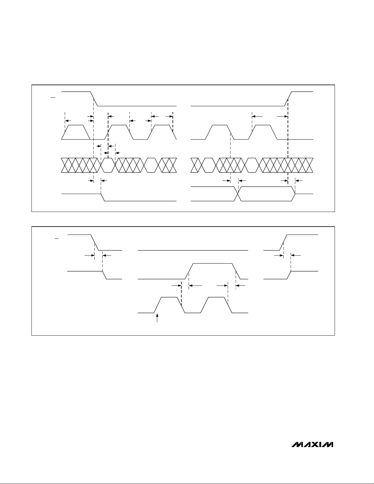
Figure 6. 24-Bit External Clock Mode Conversion Timing (MICROWIRE and SPI Compatible)
Simple Software Interface
Make sure the CPU’s serial interface runs in master
mode so the CPU generates the serial clock. Choose a
clock frequency from 100kHz to 2MHz.
1) Set up the control byte for external clock mode and
call it TB1. TB1’s format should be: 1XXXXX11 binary,
where the Xs denote the particular channel and
conversion mode selected.
2) Use a general-purpose I/O line on the CPU to pull
CS on the MAX1202/MAX1203 low.
3) Transmit TB1 and simultaneously receive a byte
and call it RB1. Ignore RB1.
4) Transmit a byte of all zeros ($00 hex) and simultaneously receive byte RB2.
5) Transmit a byte of all zeros ($00 hex) and simultaneously receive byte RB3.
6) Pull CS on the MAX1202/MAX1203 high.
Figure 6 shows the timing for this sequence. Bytes RB2
and RB3 contain the result of the conversion padded with
one leading zero and three trailing zeros. The total conversion time is a function of the serial-clock frequency and
the amount of idle time between 8-bit transfers. To avoid
excessive T/H droop, make sure that the total conversion
time does not exceed 120µs.
Digital Output
In unipolar-input mode, the output is straight binary
(Figure 15); for bipolar inputs, the output is two’scomplement (Figure 16). Data is clocked out at SCLK’s
falling edge in MSB-first format. The digital output logic
level is adjusted with the VL pin. This allows DOUT and
SSTRB to interface with 3V logic without the risk of
overdrive. The MAX1202/MAX1203’s digital inputs are
designed to be compatible with 5V CMOS logic as well
as 3V logic.
Internal and External Clock Modes
The MAX1202/MAX1203 can use either an external serial clock or the internal clock to perform the successiveapproximation conversion. In both clock modes, the
external clock shifts data in and out of the MAX1202/
MAX1203. The T/H acquires the input signal as the last
three bits of the control byte are clocked into DIN. Bits
PD1 and PD0 of the control byte program the clock
mode. Figures 7–10 show the timing characteristics
common to both modes.
External Clock
In external clock mode, the external clock not only shifts
data in and out, but it also drives the A/D conversion
steps. SSTRB pulses high for one clock period after the
last bit of the control byte. Successive-approximation bit
decisions are made and appear at DOUT on each of the
next 12 SCLK falling edges (Figure 6). SSTRB and
DOUT go into a high-impedance state when CS goes
high; after the next CS falling edge, SSTRB outputs a
logic low. Figure 8 shows SSTRB timing in external clock
mode.
SSTRB
SCLK
DIN
DOUT
14 8 12 16 20 24
START
SEL2 SEL1 SEL0
UNI/
BIP
SGL/
DIF
PD1 PD0
B11
MSB
B10 B9 B8 B7 B6 B5 B4 B3 B2 B1
B0
LSB
1.5µs
(SCLK = 2MHz)
IDLE
FILLED WITH
ZEROS
IDLE
CONVERSION
t
ACQ
ADC STATE
CS
RB1
RB2
RB3
ACQUISITION
MAX1202/MAX1203
5V, 8-Channel, Serial, 12-Bit ADCs
with 3V Digital Interface
14 ______________________________________________________________________________________
Figure 8. External Clock Mode SSTRB Detailed Timing
• • •
• • •
• • •
• • •
t
SDV
t
SSTRB
PD0 CLOCKED IN
t
STR
SSTRB
SCLK
CS
t
SSTRB
• • •
• • •
Figure 7. Detailed Serial-Interface Timing
• • •
• • •
• • •
• • •
CS
SCLK
DIN
DOUT
t
CSH
t
CSS
t
CL
t
DS
t
DH
t
DV
t
CH
t
DO
t
TR
t
CSH
The conversion must complete in some minimum time or
droop on the sample-and-hold capacitors might degrade
conversion results. Use internal clock mode if the clock
period exceeds 10µs or if serial-clock interruptions could
cause the conversion interval to exceed 120µs.
Internal Clock
In internal clock mode, the MAX1202/MAX1203 generate
their own conversion clock. This frees the µP from running the SAR conversion clock, and allows the conversion results to be read back at the processor’s
convenience, at any clock rate from zero to 2MHz.
SSTRB goes low at the start of the conversion, then goes
high when the conversion is complete. SSTRB is low for
a maximum of 10µs, during which time SCLK should
remain low for best noise performance. An internal register stores data while the conversion is in progress. SCLK
clocks the data out at this register at any time after the
conversion is complete. After SSTRB goes high, the next
falling clock edge produces the MSB of the conversion
at DOUT, followed by the remaining bits in MSB-first format (Figure 9). CS does not need to be held low once a

MAX1202/MAX1203
5V, 8-Channel, Serial, 12-Bit ADCs
with 3V Digital Interface
______________________________________________________________________________________ 15
Figure 9. Internal Clock Mode Timing
SSTRB
CS
SCLK
DIN
DOUT
14 8
12
18
20
24
START
SEL2 SEL1 SEL0
UNI/
BIP
SGL/
DIF
PD1 PD0
B11
MSB
B10 B9 B2 B1
B0
LSB
ACQUISITION
1.5µs
(SCLK = 2MHz)
IDLE
FILLED WITH
ZEROS
IDLE
CONVERSION
10µs MAX
ADC STATE
2 3 5 6 7 9 10 11 19 21 22 23
t
CONV
Figure 10. Internal Clock Mode SSTRB Detailed Timing
PD0 CLOCK IN
t
SSTRB
t
CSH
t
CONV
t
SCK
SSTRB • • •
SCLK • • •
t
CSS
NOTE: KEEP SCLK LOW DURING CONVERSION FOR BEST NOISE PERFORMANCE.
CS • • •
conversion is started. Pulling CS high prevents data from
being clocked into the MAX1202/MAX1203 and threestates DOUT, but it does not adversely affect an internal
clock mode conversion already in progress. When
internal clock mode is selected, SSTRB does not go into
a high-impedance state when CS goes high.
Figure 10 shows SSTRB timing in internal clock mode.
Data can be shifted in and out of the MAX1202/MAX1203
at clock rates up to 2.0MHz, if t
ACQ
is kept above 1.5µs.
Data Framing
CS’s falling edge does not start a conversion on the
MAX1202/MAX1203. The first logic high clocked into DIN
is interpreted as a start bit and defines the first bit of the
control byte. A conversion starts on SCLK’s falling edge
after the eighth bit of the control byte (the PD0 bit) is
clocked into DIN. The start bit is defined as one of the
following:
The first high bit clocked into DIN with CS low anytime the converter is idle (e.g., after V
DD
is applied).
or
The first high bit clocked into DIN after bit 5 (B5) of a
conversion in progress appears at DOUT.
If a falling edge on CS forces a start bit before B5
becomes available, the current conversion is terminated and a new one started. Thus, the fastest the
MAX1202/MAX1203 can run is 15 clocks/conversion.

MAX1202/MAX1203
5V, 8-Channel, Serial, 12-Bit ADCs
with 3V Digital Interface
16 ______________________________________________________________________________________
Figure 11a shows the serial-interface timing necessary
to perform a conversion every 15 SCLK cycles in external clock mode. If CS is low and SCLK is continuous,
guarantee a start bit by first clocking in 16 zeros.
Most microcontrollers (µCs) require that data transfers
occur in multiples of eight clock cycles; 16 clocks per
conversion is typically the fastest that a µC can drive
the MAX1202/MAX1203. Figure 11b shows the
serial-interface timing necessary to perform a conversion every 16 SCLK cycles in external clock mode.
__________ Applications Information
Power-On Reset
When power is first applied and if SHDN is not pulled
low, internal power-on reset circuitry activates the
MAX1202/MAX1203 in internal clock mode, ready to
convert with SSTRB = high. After the power supplies
are stabilized, the internal reset time is 100µs. No conversions should be performed during this phase.
SSTRB is high on power-up, and if CS is low, the first
logical 1 on DIN is interpreted as a start bit. Until a conversion takes place, DOUT shifts out zeros.
Reference-Buffer Compensation
In addition to its shutdown function, SHDN also selects
internal or external compensation. The compensation
affects both power-up time and maximum conversion
speed. Compensated or not, the minimum clock rate is
100kHz due to droop on the sample-and-hold.
Float SHDN to select external compensation. The
Typical Operating Circuit
uses a 4.7µF capacitor at REF.
A value of 4.7µF or greater ensures stability and allows
converter operation at the 2MHz full clock speed.
External compensation increases power-up time (see
the section
Choosing Power-Down Mode,
and Table 5).
Internal compensation requires no external capacitor at
REF, and is selected by pulling SHDN high. Internal
compensation allows for the shortest power-up times,
but the external clock must be limited to 400kHz during
the conversion.
Power-Down
Choosing Power-Down Mode
You can save power by placing the converter in a lowcurrent shutdown state between conversions. Select full
power-down or fast power-down mode via bits 1 and 0
of the DIN control byte with SHDN high or floating
(Tables 2 and 6). Pull SHDN low at any time to shut
down the converter completely. SHDN overrides bits 1
and 0 of the control byte.
Full power-down mode turns off all chip functions that draw
quiescent current, reducing IDDand ISStypically to 2µA.
For the MAX1202, fast power-down mode turns off all
circuitry except the bandgap reference. With fast
power-down mode, the supply current is 30µA. Power-up
time can be shortened to 5µs in internal compensation
mode.
Since the MAX1203 does not have an internal reference,
power-up times coming out of full or fast power-down are
identical.
I
DD
shutdown current can increase if any digital input
(DIN, SCLK, CS) is held high in either power-down
mode. The actual shutdown current depends on the
state of the digital inputs, the voltage applied to the digital inputs (VIH), the supply voltage (VDD), and the operat-
ing temperature. Figure 12c shows the maximum I
DD
increase for each digital input held high in power-down
mode for different operating conditions. This current is
cumulative, so if all three digital inputs are held high, the
additional shutdown current is three times the value
shown in Figure 12c.
In both software power-down modes, the serial interface
remains operational, but the ADC does not convert.
Table 5 shows how the choice of reference-buffer compensation and power-down mode affects both power-up
delay and maximum sample rate. In external compensation mode, power-up time is 20ms with a 4.7µF compensation capacitor (200ms with a 33µF capacitor) when the
capacitor is initially fully discharged. From fast
power-down, start-up time can be eliminated by using
low-leakage capacitors that do not discharge more than
1/2LSB while shut down. In power-down, the capacitor
has to supply the current into the reference (typically
1.5µA) and the transient currents at power-up.
Figures 12a and 12b show the various power-down
sequences in both external and internal clock modes.
Software Power-Down
Software power-down is activated using bits PD1 and
PD0 of the control byte. As shown in Table 6, PD1 and
PD0 also specify the clock mode. When software
power-down is asserted, the ADC continues to operate
in the last specified clock mode until the conversion is
complete. The ADC then powers down into a low quiescent-current state. In internal clock mode, the interface
remains active and conversion results can be clocked
out even though the MAX1202/MAX1203 have already
entered software power-down.
The first logical 1 on DIN is interpreted as a start bit and
powers up the MAX1202/MAX1203. Following the start
bit, the control byte also determines clock and
power-down modes. For example, if the DIN word contains PD1 = 1, the chip remains powered up. If PD1 = 0,
power-down resumes after one conversion.

MAX1202/MAX1203
5V, 8-Channel, Serial, 12-Bit ADCs
with 3V Digital Interface
______________________________________________________________________________________ 17
Figure 11a. External Clock Mode, 15 Clocks/Conversion Timing
Figure 11b. External Clock Mode, 16 Clocks/Conversion Timing
Hardware Power-Down
The SHDN pin places the converter into full power-down
mode. Unlike the software power-down modes, conversion is not completed; it stops coincidentally with SHDN
being brought low. There is no power-up delay if an
external reference, which is not shut down, is used.
SHDN also selects internal or external reference compensation (Table 7).
Power-Down Sequencing
The MAX1202/MAX1203’s automatic power-down
modes can save considerable power when operating
at less than maximum sample rates. The following sections discuss the various power-down sequences.
Lowest Power at up to
500 Conversions per Channel per Second
Figure 14a depicts MAX1202 power consumption for one
or eight channel conversions using full power-down
mode and internal reference compensation. A 0.01µF
bypass capacitor at REFADJ forms an RC filter with the
internal 20kΩ reference resistor, with a 0.2ms time constant. To achieve full 12-bit accuracy, 10 time constants
(or 2ms in this example) are required for the reference
buffer to settle. When exiting FULLPD, waiting this 2ms in
FASTPD mode (instead of just exiting FULLPD mode and
returning to normal operating mode) reduces power consumption by a factor of 10 or more (Figure 13).
Lowest Power at Higher Throughputs
Figure 14b shows power consumption with externalreference compensation in fast power-down, with one
and eight channels converted. The external 4.7µF compensation requires a 50µs wait after power-up. This circuit combines fast multichannel conversion with the
lowest power consumption possible. Full power-down
mode can increase power savings in applications where
the MAX1202/MAX1203 are inactive for long periods of
time, but where intermittent bursts of high-speed conversion are required.
SCLK
DIN
DOUT
CS
S CONTROL BYTE 0
CONTROL BYTE 1S
CONVERSION RESULT 0
CONVERSION RESULT 1
SSTRB
CONTROL BYTE 2S
1
8181
B4B5B6B7B8B9B10B11 B3 B2 B1 B0 B4B5B6B7B8B9B10B11 B3 B2 B1 B0
CS
SCLK
DIN
DOUT
S CONTROL BYTE 0
CONVERSION RESULT 0
B2B3B4B5B6B7B8B9B10B11 B5B6B7B8B9B10B11B1 B0
CONTROL BYTE 1S
CONVERSION RESULT 1
• • •
• • •
• • •
• • •

MAX1202/MAX1203
5V, 8-Channel, Serial, 12-Bit ADCs
with 3V Digital Interface
18 ______________________________________________________________________________________
Table 6. Software Shutdown
and Clock Mode
Table 5. Typical Power-Up Delay Times
Table 7. Hard-Wired Shutdown
and Compensation Mode
Figure 12a. Timing Diagram for Power-Down Modes, External Clock
POWERED UP
FULL
POWER-
DOWN
POWERED
UP
POWERED UP
DATA VALID
(12 DATA BITS)
DATA VALID
(12 DATA BITS)
DATA
INVALID
EXTERNAL
EXTERNAL
INTERNAL
SX
XXXX
11 S 01
XXXXX XXXXX
S11
FAST
POWER-DOWN
MODE
DOUT
DIN
CLOCK
MODE
SHDN
SETS EXTERNAL
CLOCK MODE
SETS EXTERNAL
CLOCK MODE
SETS FAST
POWER-DOWN
MODE
1332FullDisabled
1332FastDisabled
133
26
26
MAXIMUM
SAMPLING RATE
(ksps)
See Figure 14c
300
5
POWER-UP
DELAY
(µs)
Fast/Full
Full
Fast
POWER-DOWN
MODE
4.7
REF
CAPACITOR
(µF)
ExternalEnabled
REFERENCE
BUFFER
InternalEnabled
InternalEnabled
REFERENCE-BUFFER
COMPENSATION MODE
N/A
Full
Power-Down
GND
SSHHDDNN
STATE
External compensationEnabledFloating
Internal compensationEnabledV
DD
REFERENCE-BUFFER
COMPENSATION
DEVICE
MODE
External clock mode11
Internal clock mode01
PD1
Fast power-down mode10
Full power-down mode00
DEVICE MODEPD0

MAX1202/MAX1203
5V, 8-Channel, Serial, 12-Bit ADCs
with 3V Digital Interface
______________________________________________________________________________________ 19
External and Internal References
The MAX1202 can be used with an internal or external
reference, whereas an external reference is required for
the MAX1203. An external reference can be connected
directly at the REF terminal, or at the REFADJ pin.
An internal buffer is designed to provide 4.096V at
REF for both the MAX1202 and the MAX1203. The
MAX1202’s internally trimmed 2.44V reference is
buffered with a gain of 1.68. The MAX1203’s REFADJ
pin is buffered with a gain of 1.64, to scale an external
2.5V reference at REFADJ to 4.096V at REF.
MAX1202 Internal Reference
The MAX1202’s full-scale range using the internal
reference is 4.096V with unipolar inputs and ±2.048V
with bipolar inputs. The internal reference voltage is
adjustable to ±1.5% with the circuit of Figure 17.
Figure 12b. Timing Diagram for Power-Down Modes, Internal Clock
Figure 12c. Additional IDDShutdown Supply Current vs. V
IH
for Each Digital Input at a Logic 1
Figure 13. MAX1202 FULLPD/FASTPD Power-Up Sequence
FULL
POWER-DOWN
POWERED
UP
POWERED UP
DATA VALID
DATA VALID
INTERNAL CLOCK MODE
SX
XXXX
10 S 00
XXXXX
S
MODE
DOUT
DIN
CLOCK
MODE
SETS INTERNAL
CLOCK MODE
SETS FULL
POWER-DOWN
CONVERSION
CONVERSION
SSTRB
40
35
30
25
20
15
10
SUPPLY CURRENT PER INPUT (µA)
5
0
(V
- VIH) = 2.55V
DD
(V
DD
(VDD - VIH) = 1.95V
20
-20 60 140
-60
TEMPERATURE (°C)
- VIH) = 2.25V
100
COMPLETE CONVERSION SEQUENCE
DIN
100
FULLPD FASTPD NOPD FULLPD FASTPD
REFADJ
REF
2.5V
0V
4V
0V
(ZEROS)
2ms WAIT
101 1 11100 101
τ = RC = 20kΩ x C
REFADJ
CH1 CH7
t
≈ 15µs
BUFFEN
(ZEROS)

MAX1202/MAX1203
5V, 8-Channel, Serial, 12-Bit ADCs
with 3V Digital Interface
20 ______________________________________________________________________________________
Figure 14a. MAX1202 Supply Current vs. Sample Rate/Second,
FULLPD, 400kHz Clock
Figure 14b. MAX1202/MAX1203 Supply Current vs. Sample
Rate/Second, FASTPD, 2MHz Clock
External Reference
With both the MAX1202 and MAX1203, an external reference can be placed at either the input (REFADJ) or the
output (REF) of the internal reference-buffer amplifier. The
REFADJ input impedance is typically 20kΩ for the
MAX1202, and higher than 100kΩ for the MAX1203,
where the internal reference is omitted. At REF, the DC
input resistance is a minimum of 12kΩ. During conversion,
an external reference at REF must deliver up to 350µA DC
load current and have an output impedance of 10Ω or
less. If the reference has higher output impedance or is
noisy, bypass it close to the REF pin with a 4.7µF capacitor.
Using the buffered REFADJ input makes buffering of the
external reference unnecessary. When connecting an
external reference directly at REF, disable the internal
buffer by tying REFADJ to VDD. In power-down, the input
bias current to REFADJ can be as much as 25µA with
REFADJ tied to V
DD
(MAX1202 only). Pull REFADJ to
GND to minimize the input bias current in power-down.
Transfer Function and Gain Adjust
Figure 15 depicts the nominal, unipolar input/output
(I/O) transfer function, and Figure 16 shows the bipolar
I/O transfer function. Code transitions occur halfway
between successive-integer LSB values. Output coding
is binary with 1LSB = 1.00mV (4.096V/4096) for unipolar operation, and 1LSB = 1.00mV [(4.096V/2 - -4.096V/
2)/4096] for bipolar operation.
Figure 17 shows how to adjust the ADC gain in applica-
tions that use the internal reference. The circuit provides
±1.5% (±65LSBs) of gain adjustment range.
Layout, Grounding, and Bypassing
For best performance, use printed circuit boards.
Wire-wrap boards are not recommended. Board layout
should ensure that digital and analog signal lines are
separated from each other. Do not run analog and digital (especially clock) lines parallel to one another, or
digital lines underneath the ADC package.
Figure 18 shows the recommended system ground
connections. Establish a single-point analog ground
1000
1
0 100 300 500
FULL POWER-DOWN
10
100
MAX186-14A
CONVERSIONS PER CHANNEL PER SECOND
200 400
2ms FASTPD WAIT
400kHz EXTERNAL CLOCK
INTERNAL COMPENSATION
50 150 250 350 450
8 CHANNELS
1 CHANNEL
AVERAGE SUPPLY CURRENT (µA)
Figure 14c. Typical Power-Up Delay vs. Time in Shutdown
10,000
1000
100
AVERAGE SUPPLY CURRENT (µA)
10
0
2k
MAX1202/MAX1203
FAST POWER-DOWN
8 CHANNELS
1 CHANNEL
2MHz EXTERNAL CLOCK
EXTERNAL COMPENSATION
50µs WAIT
4k 6k 8k 10k 12k 14k 16k 18k
CONVERSIONS PER CHANNEL PER SECOND
3.0
2.5
2.0
1.5
1.0
POWER-UP DELAY (ms)
0.5
0
0.0001 0.001 0.01 0.1 1 10
TIME IN SHUTDOWN (sec)

MAX1202/MAX1203
5V, 8-Channel, Serial, 12-Bit ADCs
with 3V Digital Interface
______________________________________________________________________________________ 21
Figure 16. Bipolar Transfer Function, ±4.096V/2 = Full ScaleFigure 15. Unipolar Transfer Function, 4.096V = Full Scale
(“star” ground point) at GND. Connect all other analog
grounds to this ground. No other digital system ground
should be connected to this single-point analog
ground. The ground return to the power supply for this
ground should be low impedance and as short as possible for noise-free operation.
High-frequency noise in the power supplies can affect
the ADC’s high-speed comparator. Bypass these supplies to the single-point analog ground with 0.1µF and
4.7µF bypass capacitors close to the
MAX1202/MAX1203. Minimize capacitor lead lengths
for best supply-noise rejection. If the +5V power supply
is very noisy, a 10Ω resistor can be connected as a
lowpass filter, as shown in Figure 18.
OUTPUT CODE
FULL-SCALE
TRANSITION
11 . . . 111
11 . . . 110
11 . . . 101
00 . . . 011
00 . . . 010
00 . . . 001
00 . . . 000
123
0
FS
FS - 3/2LSB
+4.096V
+
4.096V
4096
FS =
1LSB =
INPUT VOLTAGE (LSBs)
Figure 17. MAX1202 Reference-Adjust Circuit
OUTPUT CODE
011 . . . 111
011 . . . 110
000 . . . 010
000 . . . 001
000 . . . 000
111 . . . 111
111 . . . 110
111 . . . 101
100 . . . 001
100 . . . 000
FS = +2.048V
+4.096V
1LSB =
4096
-FS
0V
INPUT VOLTAGE (LSBs)
+5V
510k
100k
24k
0.01µF
12
+FS - 1LSB
MAX1202
REFADJ
MAX1202/MAX1203
5V, 8-Channel, Serial, 12-Bit ADCs
with 3V Digital Interface
22 ______________________________________________________________________________________
TMS320CL3x to MAX1202/
MAX1203 Interface
Figure 19 shows an application circuit to interface the
MAX1202/MAX1203 to the TMS320 in external clock mode.
Figure 20 shows the timing diagram for this interface circuit.
Use the following steps to initiate a conversion in the
MAX1202/MAX1203 and to read the results:
1) The TMS320 should be configured with CLKX (transmit clock) as an active-high output clock and CLKR
(TMS320 receive clock) as an active-high input clock.
The TMS320’s CLKX and CLKR are tied together with
the MAX1202/MAX1203’s SCLK input.
2) The MAX1202/MAX1203’s CS is driven low by the
TMS320’s XF_ I/O port to enable data to be clocked
into the MAX1202/MAX1203’s DIN.
3) Write an 8-bit word (1XXXXX11) to the MAX1202/
MAX1203 to initiate a conversion and place the
device into external clock mode. Refer to Table 2 to
select the proper XXXXX bit values for your specific
application.
4) The MAX1202/MAX1203’s SSTRB output is monitored via the TMS320’s FSR input. A falling edge on
the SSTRB output indicates that the conversion is in
progress and data is ready to be received from the
MAX1202/MAX1203.
5) The TMS320 reads in one data bit on each of the
next 16 rising edges of SCLK. These data bits represent the 12-bit conversion result followed by four
trailing bits, which should be ignored.
6) Pull CS high to disable the MAX1202/MAX1203 until
the next conversion is initiated.
Figure 19. MAX1202/MAX1203-to-TMS320 Serial Interface
+5V
-5V +3V
GND
SUPPLIES
DGND+3VVLV
SS
GNDV
DD
DIGITAL
CIRCUITRY
MAX1202
MAX1203
R* = 10Ω
*OPTIONAL
Figure 18. Power-Supply Grounding Connection
Figure 20. TMS320 Serial-Interface Timing Diagram
CS
SCLK
DIN
SSTRB
DOUT
START SEL2 SEL1 SEL0 UNI/BIP SGL/DIF PD1 PD0
MSB B10 B1 LSB
HIGH
IMPEDANCE
HIGH
IMPEDANCE
XF
CLKX
TMS320LC3x
CLKR
DX
CS
SCLK
MAX1202
MAX1203
DIN
DR
FSR
DOUT
SSTRB

MAX1202/MAX1203
5V, 8-Channel, Serial, 12-Bit ADCs
with 3V Digital Interface
______________________________________________________________________________________ 23
_Ordering Information (continued)
V
DD
I/O
SCK (SK)
MOSI (SO)
MISO (SI)
V
SS
SHDN
SSTRB
DOUT
DIN
SCLK
CS
V
SS
VL
GND
V
DD
REFADJ
CH7
C3
0.1µF
C4
4.7µF
C5
0.1µF
CH0
+3V
+5V
C2
0.01µF
0V to
4.096V
ANALOG
INPUTS
MAX1202
CPU
C1
4.7µF
REF
__________Typical Operating Circuit
___________________Chip Information
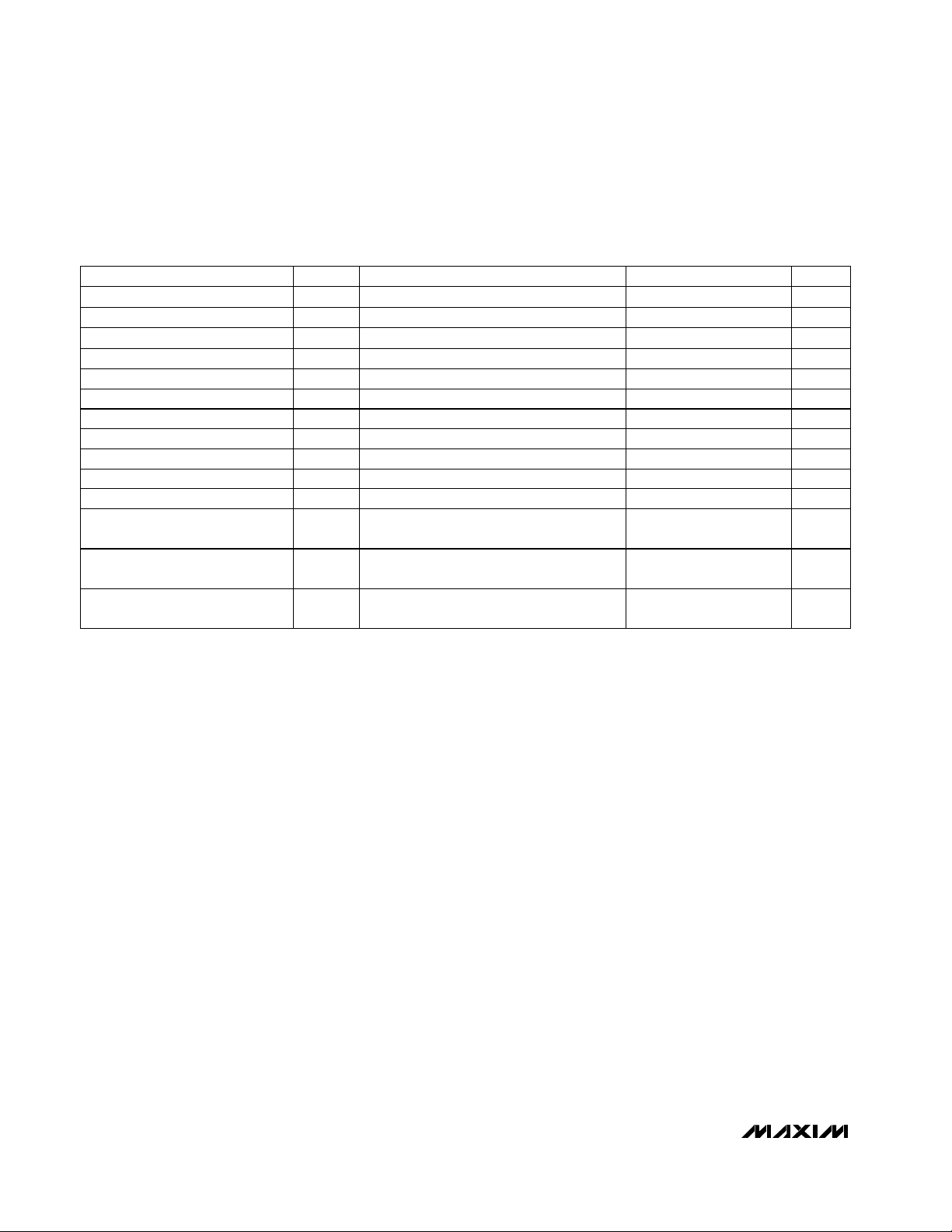
*
Dice are specified at TA= +25°C, DC parameters only.
**
Contact factory for availability.
TRANSISTOR COUNT: 2503
SUBSTRATE CONNECTED TO V
SS
PART
MAX1202AEPP
MAX1202BEPP
MAX1202AEAP -40°C to +85°C
-40°C to +85°C
-40°C to +85°C
TEMP. RANGE PIN-PACKAGE
20 Plastic DIP
20 Plastic DIP
20 SSOP
MAX1202BEAP -40°C to +85°C 20 SSOP
MAX1202BMJP -55°C to +125°C 20 CERDIP**
INL
(LSB)
±1/2
±1
±1/2
±1
±1
MAX1203ACPP
MAX1203BCPP
MAX1203ACAP 0°C to +70°C
0°C to +70°C
0°C to +70°C 20 Plastic DIP
20 Plastic DIP
20 SSOP
MAX1203BCAP 0°C to +70°C 20 SSOP
MAX1203BC/D 0°C to +70°C Dice*
±1/2
±1
±1/2
±1
±1
MAX1203AEPP
MAX1203BEPP
MAX1203AEAP -40°C to +85°C
-40°C to +85°C
-40°C to +85°C 20 Plastic DIP
20 Plastic DIP
20 SSOP
MAX1203BEAP -40°C to +85°C 20 SSOP
MAX1203BMJP -55°C to +125°C 20 CERDIP**
±1/2
±1
±1/2
±1
±1

Maxim cannot assume responsibility for use of any circuitry other than circuitry entirely embodied in a Maxim product. No circuit patent licenses are
implied. Maxim reserves the right to change the circuitry and specifications without notice at any time.
24
__________________Maxim Integrated Products, 120 San Gabriel Drive, Sunnyvale, CA 94086 (408) 737-7600
© 1998 Maxim Integrated Products Printed USA is a registered trademark of Maxim Integrated Products.
MAX1202/MAX1203
5V, 8-Channel, Serial, 12-Bit ADCs
with 3V Digital Interface
________________________________________________________Package Information
PDIPN.EPS
SSOP.EPS
 Loading...