

General Description
The MAX1193 is an ultra-low-power, dual, 8-bit,
45Msps analog-to-digital converter (ADC). The device
features two fully differential wideband track-and-hold
(T/H) inputs. These inputs have a 440MHz bandwidth
and accept fully differential or single-ended signals.
The MAX1193 delivers a typical signal-to-noise and distortion (SINAD) of 48.5dB at an input frequency of
5.5MHz and a sampling rate of 45Msps while consuming only 57mW. This ADC operates from a 2.7V to 3.6V
analog power supply. A separate 1.8V to 3.6V supply
powers the digital output driver. In addition to ultra-low
operating power, the MAX1193 features three powerdown modes to conserve power during idle periods.
Excellent dynamic performance, ultra-low power, and
small size make the MAX1193 ideal for applications in
imaging, instrumentation, and digital communications.
An internal 1.024V precision bandgap reference sets
the full-scale range of the ADC to ±0.512V. A flexible
reference structure allows the MAX1193 to use its internal reference or accept an externally applied reference
for applications requiring increased accuracy.
The MAX1193 features parallel, multiplexed, CMOScompatible tri-state outputs. The digital output format is
offset binary. A separate digital power input accepts a
voltage from 1.8V to 3.6V for flexible interfacing to different logic levels. The MAX1193 is available in a 5mm
× 5mm, 28-pin thin QFN package, and is specified for
the extended industrial (-40°C to +85°C) temperature
range.
For higher sampling frequency applications, refer to the
MAX1195–MAX1198 dual 8-bit ADCs. Pin-compatible
versions of the MAX1193 are also available. Refer to the
MAX1191 data sheet for 7.5Msps, and the MAX1192
data sheet for 22Msps.
Applications
Ultrasound and Medical Imaging
IQ Baseband Sampling
Battery-Powered Portable Instruments
Low-Power Video
WLAN, Mobile DSL, WLL Receiver
Features
♦ Ultra-Low Power
57mW (Normal Operation: 45Msps)
0.3µW (Shutdown Mode)
♦ Excellent Dynamic Performance
48.5dB/48.3dB SNR at f
IN
= 5.5MHz/100MHz
70dBc/68dBc SFDR at f
IN
= 5.5MHz/100MHz
♦ 2.7V to 3.6V Single Analog Supply
♦ 1.8V to 3.6V TTL/CMOS-Compatible Digital
Outputs
♦ Fully Differential or Single-Ended Analog Inputs
♦ Internal/External Reference Option
♦ Multiplexed CMOS-Compatible Tri-State Outputs
♦ 28-Pin Thin QFN Package
♦ Evaluation Kit Available (Order MAX1193EVKIT)
MAX1193
Ultra-Low-Power, 45Msps, Dual 8-Bit ADC
________________________________________________________________ Maxim Integrated Products 1
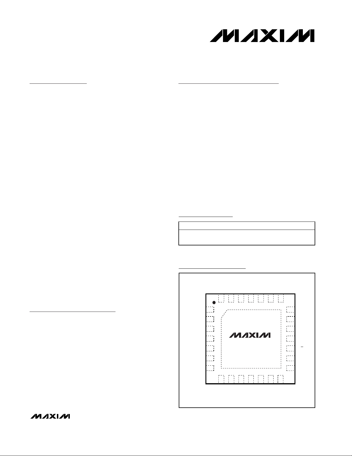
Pin Configuration
Ordering Information
19-2794; Rev 1; 9/03
For pricing, delivery, and ordering information, please contact Maxim/Dallas Direct! at
1-888-629-4642, or visit Maxim’s website at www.maxim-ic.com.
*EP = Exposed paddle.
PART TEMP RANGE PIN-PACKAGE
MAX1193ETI-T -40°C to +85°C
28 Thin QFN-EP*
(5mm x 5mm)
TOP VIEW
DD
V
REFP
REFN
COM
REFIN
PD0
PD1
28
27
26
25
24
23
22
INA-
INA+
GND
CLK
GND
INB+
INB-
1
2
3
4
5
6
7
MAX1193
EXPOSED PADDLE
D0
21
20
D1
19
D2
18
D3
17
A/B
16
D4
D5
15
8
9
10
11
12
13
14
DD
DD
V
V
5mm x 5mm THIN QFN
GND
OGND
DD
D7
OV
D6
MAX1193
Ultra-Low-Power, 45Msps, Dual 8-Bit ADC
2 _______________________________________________________________________________________
ABSOLUTE MAXIMUM RATINGS
ELECTRICAL CHARACTERISTICS
(VDD= 3.0V, OVDD= 1.8V, V
REFIN
= VDD(internal reference), CL≈ 10pF at digital outputs, f
CLK
= 45MHz, C
REFP
= C
REFN
= C
COM
=
0.33µF, T
A
= -40°C to +85°C, unless otherwise noted. Typical values are at TA = +25°C.) (Note 1)
Stresses beyond those listed under “Absolute Maximum Ratings” may cause permanent damage to the device. These are stress ratings only, and functional
operation of the device at these or any other conditions beyond those indicated in the operational sections of the specifications is not implied. Exposure to
absolute maximum rating conditions for extended periods may affect device reliability.
VDD, OVDDto GND ...............................................-0.3V to +3.6V
OGND to GND.......................................................-0.3V to +0.3V
INA+, INA-, INB+, INB- to GND .................-0.3V to (V
DD
+ 0.3V)
CLK, REFIN, REFP, REFN, COM to GND ...-0.3V to (V
DD
+ 0.3V)
PD0, PD1 to OGND .................................-0.3V to (OV
DD
+ 0.3V)
Digital Outputs to OGND.........................-0.3V to (OV
DD
+ 0.3V)
Continuous Power Dissipation (T
A
= +70°C)
28-Pin Thin QFN (derated 20.8mW/°C above +70°C) ..1667mW
Operating Temperature Range ...........................-40°C to +85°C
Junction Temperature......................................................+150°C
Storage Temperature Range .............................-65°C to +150°C
Lead Temperature (soldering, 10s) .................................+300°C
DC ACCURACY
Resolution 8 Bits
Integral Nonlinearity INL ±0.16 ±1.00 LSB
Differential Nonlinearity DNL No missing codes over temperature ±0.15 ±1.00 LSB
Offset Error
Gain Error Excludes REFP - REFN error ±2 %FS
DC Gain Matching ±0.01 ±0.2 dB
Gain Temperature Coefficient ±30 p p m /°C
Power-Supply Rejection
ANALOG INPUT
Differential Input Voltage Range V
Common-Mode Input Voltage
Range
Input Resistance R
Input Capacitance C
CONVERSION RATE
Maximum Clock Frequency f
Data Latency
DYNAMIC CHARACTERISTICS (differential inputs, 4096-point FFT)
Signal-to-Noise Ratio
(Note 2)
Signal-to-Noise and Distortion
(Note 2)
PARAMETER SYMBOL CONDITIONS MIN TYP MAX UNITS
≥ +25°C ±4
< +25°C ±6
Offset (VDD ±5%) ±0.2
DIFF
V
COM
IN
IN
CLK
SNR
SINAD
Gain (V
Differential or single-ended inputs ±0.512 V
Switched capacitor load 120 kΩ
Channel A 5.0
Channel B 5.5
fIN = 3.75MHz 48.5
fIN = 5.5MHz 47 48.5
f
IN
fIN = 3.75MHz 48.5
fIN = 5.5MHz 47 48.5
f
IN
±5%) ±0.05
DD
= 22.5MHz 48.4
= 22.5MHz 48.4
VDD / 2 V
45 MHz
5pF
%FS
LSB
Clock
cycles
dB
dB
MAX1193
Ultra-Low-Power, 45Msps, Dual 8-Bit ADC
_______________________________________________________________________________________ 3
ELECTRICAL CHARACTERISTICS (continued)
(VDD= 3.0V, OVDD= 1.8V, V
REFIN
= VDD(internal reference), CL≈ 10pF at digital outputs, f
CLK
= 45MHz, C
REFP
= C
REFN
= C
COM
=
0.33µF, T
A
= -40°C to +85°C, unless otherwise noted. Typical values are at TA = +25°C.) (Note 1)
PARAMETER SYMBOL CONDITIONS MIN TYP MAX UNITS
Spurious-Free Dynamic Range
(Note 2)
Thi r d - H ar m oni c D i stor ti on
( N ote 2)
Intermodulation Distortion IMD
Third-Order Intermodulation IM3
Total Harmonic Distortion
(Note 2)
Small-Signal Bandwidth SSBW Input at -20dB FS 440 MHz
Full-Power Bandwidth FPBW Input at -0.5dB FS 440 MHz
Aperture Delay t
Aperture Jitter t
Overdrive Recovery Time 1.5 × full-scale input 2 ns
INTERNAL REFERENCE (REFIN = VDD; V
REFP Output Voltage V
REFN Output Voltage V
COM Output Voltage V
Differential Reference Output V
Differential Reference Output
Temperature Coefficient
Maximum REFP/REFN/COM
Source Current
Maximum REFP/REFN/COM Sink
Current
B U F FERED EXT ER N A L R EF ER EN C E ( V
REFIN Input Voltage V
COM Output Voltage V
Differential Reference Output V
Maximum REFP/REFN/COM
Source Current
fIN = 3.75MHz 70.7
SFDR
fIN = 5.5MHz 60.0 70.0
= 22.5MHz 71.5
f
IN
fIN = 3.75MHz -79.6
HD3
fIN = 5.5MHz -79.0
= 22.5MHz 76.1
f
IN
f
= 1MHz at -7dB FS, f
IN1
= 1.01MHz
IN2
at -7dB FS
f
= 1MHz at -7dB FS, f
IN1
= 1.01MHz
IN2
at -7dB FS
fIN = 3.75MHz -70.8
THD
V
REFTC
I
SOURCE
I
I
SOURCE
fIN = 5.5MHz -70.0 -57.0
f
= 22.5MHz -70.1
IN
AD
AJ
, V
COM
REF
SINK
R E F IN
REFIN
COM
REF
REFP
REFP
REFN
V
REFP
= 1.024V , V
V
REFP
REFN
- V
- V
- V
, and V
COM
COM
REFN
- V
REFN
R E F P
are generated internally)
COM
, V
, and V
R E F N
VDD / 2
- 0.15
ar e g ener ated i nter nal l y)
C OM
VDD / 2
- 0.15
-66 dBc
-70 dBc
1.5 ns
2ps
0.256 V
-0.256 V
V
/ 2
V
/ 2
DD
DD
+ 0.15
0.512 V
±30 ppm/°C
2mA
2mA
1.024 V
/ 2
V
V
/ 2
DD
DD
+ 0.15
0.512 V
2mA
dBc
dBc
dBc
RMS
V
V
MAX1193
Ultra-Low-Power, 45Msps, Dual 8-Bit ADC
4 _______________________________________________________________________________________
ELECTRICAL CHARACTERISTICS (continued)
(VDD= 3.0V, OVDD= 1.8V, V
REFIN
= VDD(internal reference), CL≈ 10pF at digital outputs, f
CLK
= 45MHz, C
REFP
= C
REFN
= C
COM
=
0.33µF, T
A
= -40°C to +85°C, unless otherwise noted. Typical values are at TA = +25°C.) (Note 1)
PARAMETER SYMBOL CONDITIONS MIN TYP MAX UNITS
Maximum REFP/REFN/COM Sink
Current
REFIN Input Resistance >500 kΩ
REFIN Input Current -0.7 µA
UNBUFFERED EXTERNAL REFERENCE (REFIN = GND, V
REFP Input Voltage V
REFN Input Voltage V
COM Input Voltage V
Differential Reference Input
Voltage
REFP Input Resistance R
REFN Input Resistance R
DIGITAL INPUTS (CLK, PD0, PD1)
Input High Threshold V
Input Low Threshold V
Input Hysteresis V
Digital Input Leakage Current DI
Digital Input Capacitance DC
DIGITAL OUTPUTS (D7–D0, A/B)
Output Voltage Low V
Output Voltage High V
Tri-State Leakage Current I
Tri-State Output Capacitance C
POWER REQUIREMENTS
Analog Supply Voltage V
Digital Output Supply Voltage OV
I
SINK
, V
REFN
, and V
COM
V
REF
REFP
REFN
REFP
- V
V
REFP
REFN
REFP
- V
- V
COM
COM
REFN
Measured between REFP and COM 4 kΩ
Measured between REFN and COM 4 kΩ
CLK
IH
PD0, PD1
CLK
IL
PD0, PD1
HYST
CLK at GND or V
IN
PD0 and PD1 at OGND or OV
IN
OLISINK
OHISOURCE
LEAK
OUT
DD
DD
= 200µA
= 200µA
DD
DD
are applied externally)
COM
0.7 x
V
DD
0.7 x
OV
DD
0.8 x
OV
DD
2.7 3.0 3.6 V
1.8 V
2mA
0.256 V
-0.256 V
VDD / 2 V
0.512 V
0.3 x
V
DD
0.3 x
OV
0.1 V
±5
±5
5pF
0.2 x
OV
±5 µA
5pF
DD
DD
DD
V
V
µA
V
V
V
MAX1193
Ultra-Low-Power, 45Msps, Dual 8-Bit ADC
_______________________________________________________________________________________ 5
,
ELECTRICAL CHARACTERISTICS (continued)
(VDD= 3.0V, OVDD= 1.8V, V
REFIN
= VDD(internal reference), CL≈ 10pF at digital outputs, f
CLK
= 45MHz, C
REFP
= C
REFN
= C
COM
=
0.33µF, T
A
= -40°C to +85°C, unless otherwise noted. Typical values are at TA = +25°C.) (Note 1)
PARAMETER SYMBOL CONDITIONS MIN TYP MAX UNITS
Analog Supply Current I
Digital Output Supply Current
(Note 3)
TIMING CHARACTERISTICS
CLK Rise to CHA Output Data
Valid
CLK Fall to CHB Output Data
Valid
CLK Rise/Fall to A/B Rise/Fall
Time
PD1 Rise to Output Enable t
PD1 Fall to Output Disable t
CLK Duty Cycle 50 %
CLK Duty-Cycle Variation ±10 %
Wake-Up Time from Shutdown
Mode
Wake-Up Time from Standby
Mode
Digital Output Rise/Fall Time 20% to 80% 2 ns
INTERCHANNEL CHARACTERISTICS
Crosstalk Rejection
Amplitude Matching fIN = 11MHz at -0.5dB FS (Note 7) ±0.05 dB
Phase Matching fIN = 11MHz at -0.5dB FS (Note 7) ±0.2 D egr ees
Normal operating mode, fIN = 5.5MHz at
-0.5dB FS, CLK input from GND to V
Idle mode (tri-state), fIN = 5.5MHz at
-0.5dB FS, CLK input from GND to V
DD
Standby mode, CLK input from
GND to V
DD
Shutdown mode, CLK = GND or VDD,
PD0 = PD1 = OGND
Normal operating mode,
f
= 5.5MHz at -0.5dB FS, CL ≈ 10pF
IN
Idle mode (tri-state), DC input, CLK =
I
ODD
GND or V
Standby mode, DC input, CLK = GND or
V
PD0 = OGND, PD1 = OV
DD,
PD0 = OVDD, PD1 = OGND
DD
Shutdown mode, CLK = GND or VDD,
PD0 = PD1 = OGND
t
DOA
t
DOB
t
DA/B
t
WAKE, SD
t
WAKE, ST
50% of C LK to 50% of d ata) ,
Fi g ur e 5 ( N ote 4)
50% of C LK to 50% of d ata,
Fi g ur e 5 ( N ote 4)
50% of C LK to 50% of A/B,
Fi g ur e 5 ( N ote 4)
PD0 = OV
EN
DIS
PD0 = OV
DD
DD
(Note 5) 20 µs
(Note 5) 2.6 µs
f
= 11MHz at -0.5dB FS,
IN,X
= 0.3MHz at -0.5dB FS (Note 6)
f
IN,Y
DD
DD
DD
19 22.5
19
8.5
0.1 5.0 µA
5mA
0.1 5.0
0.1
0.1 5.0
1 6 8.5 ns
1 6 8.5 ns
1 6 8.5 ns
5ns
5ns
-75 dB
mA
µA
MAX1193
Ultra-Low-Power, 45Msps, Dual 8-Bit ADC
6 _______________________________________________________________________________________
Typical Operating Characteristics
(VDD= 3.0V, OVDD= 1.8V, V
REFIN
= VDD(internal reference), CL≈ 10pF at digital outputs, differential input at -0.5dB FS, f
CLK
=
45.005678MHz at 50% duty cycle, T
A
= +25°C, unless otherwise noted.)
ELECTRICAL CHARACTERISTICS (continued)
(VDD= 3.0V, OVDD= 1.8V, V
REFIN
= VDD(internal reference), CL≈ 10pF at digital outputs, f
CLK
= 45MHz, C
REFP
= C
REFN
= C
COM
=
0.33µF, T
A
= -40°C to +85°C, unless otherwise noted. Typical values are at TA=+25°C.) (Note 1)
Note 1: Specifications ≥+25°C guaranteed by production test, <+25°C guaranteed by design and characterization.
Note 2: SNR, SINAD, SFDR, HD3, and THD are based on a differential analog input voltage of -0.5dB FS referenced to the
amplitude of the digital output. SNR and THD are calculated using HD2 through HD6.
Note 3: The power consumption of the output driver is proportional to the load capacitance (CL).
Note 4: Guaranteed by design and characterization. Not production tested.
Note 5: SINAD settles to within 0.5dB of its typical value.
Note 6: Crosstalk rejection is measured by applying a high-frequency test tone to one channel and a low-frequency tone to the
second channel. FFTs are performed on each channel. The parameter is specified as power ratio of the first and second
channel FFT test tone bins.
Note 7: Amplitude/phase matching is measured by applying the same signal to each channel, and comparing the magnitude and
phase of the fundamental bin on the calculated FFT.
FFT PLOT CHANNEL A (DIFFERENTIAL
INPUTS, 8192-POINT DATA RECORD)
0
f
= 45.005678MHz
CLK
-10
= 12.531448MHz
f
INA
= 21.005678MHz
f
INB
-20
= A
= -0.5dB FS
A
INA
-30
-40
-50
AMPLITUDE (dB)
-60
-70
-80
-90
INB
HD3
025
ANALOG INPUT FREQUENCY (MHz)
HD2
MAX1193 toc01
f
INB
2015510
FFT PLOT CHANNEL B (DIFFERENTIAL
INPUTS, 8192-POINT DATA RECORD)
0
f
= 45.005678MHz
CLK
-10
= 12.531448MHz
f
INA
= 21.005678MHz
f
INB
-20
= A
= -0.5dB FS
A
INA
-30
-40
-50
AMPLITUDE (dB)
-60
-70
-80
-90
INB
HD3
HD2
025
ANALOG INPUT FREQUENCY (MHz)
f
INA
2015510
MAX1193 toc02
FFT PLOT CHANNEL A (DIFFERENTIAL
INPUTS, 8192-POINT DATA RECORD)
0
f
= 45.005678MHz
CLK
-10
= 21.005678MHz
f
INA
= 12.531448MHz
f
INB
-20
= A
A
INA
-30
-40
-50
AMPLITUDE (dB)
-60
-70
-80
-90
INB
HD2
025
ANALOG INPUT FREQUENCY (MHz)
= -0.5dB FS
f
INB
HD3
2015510
MAX1193 toc03
FFT PLOT CHANNEL B (DIFFERENTIAL
INPUTS, 8192-POINT DATA RECORD)
0
f
= 45.005678MHz
CLK
-10
= 21.005678MHz
f
INA
= 12.531448MHz
f
INB
-20
= A
= -0.5dB FS
A
INA
-30
-40
-50
AMPLITUDE (dB)
-60
-70
-80
-90
INB
HD2
HD3
025
ANALOG INPUT FREQUENCY (MHz)
2015510
MAX1193 toc04
f
INA
TWO-TONE IMD PLOT (DIFFERENTIAL
INPUTS, 8192-POINT DATA RECORD)
0
-10
-20
-30
-40
-50
AMPLITUDE (dB)
-60
-70
-80
-90
f
IN2
f
IN1
025
ANALOG INPUT FREQUENCY (MHz)
f
= 45.005678MHz
CLK
= 1.8MHz
f
IN1
= 2.3MHz
f
IN2
= 7dB FS
A
IN
MAX1193 toc05
2015510
MAX1193
Ultra-Low-Power, 45Msps, Dual 8-Bit ADC
_______________________________________________________________________________________ 7
Typical Operating Characteristics (continued)
(VDD= 3.0V, OVDD= 1.8V, V
REFIN
= VDD(internal reference), CL≈ 10pF at digital outputs, differential input at -0.5dB FS, f
CLK
=
45.005678MHz at 50% duty cycle, T
A
= +25°C, unless otherwise noted.)
SIGNAL-TO-NOISE RATIO
vs. ANALOG INPUT FREQUENCY
50.0
49.5
49.0
48.5
48.0
SNR (dB)
47.5
47.0
46.5
46.0
0 125
ANALOG INPUT FREQUENCY (MHz)
TOTAL HARMONIC DISTORTION
vs. ANALOG INPUT FREQUENCY
-45
-50
-55
-60
-65
THD (dBc)
-70
-75
-80
-85
0 125
ANALOG INPUT FREQUENCY (MHz)
SIGNAL-TO-NOISE PLUS DISTORTION
vs. ANALOG INPUT FREQUENCY
50.0
CHANNEL A
CHANNEL B
1007525 50
CHANNEL A
CHANNEL B
1007525 50
MAX1193 toc06
MAX1193 toc08
49.5
49.0
48.5
48.0
SINAD (dB)
47.5
47.0
46.5
46.0
0 125
ANALOG INPUT FREQUENCY (MHz)
CHANNEL A
CHANNEL B
SPURIOUS-FREE DYNAMIC RANGE
vs. ANALOG INPUT FREQUENCY
85
80
75
70
65
SFDR (dBc)
60
55
50
45
0 125
CHANNEL B
CHANNEL A
ANALOG INPUT FREQUENCY (MHz)
MAX1193 toc07
1007525 50
MAX1193 toc09
1007525 50
MAX1193
Ultra-Low-Power, 45Msps, Dual 8-Bit ADC
8 _______________________________________________________________________________________
Typical Operating Characteristics (continued)
(VDD= 3.0V, OVDD= 1.8V, V
REFIN
= VDD(internal reference), CL≈ 10pF at digital outputs, differential input at -0.5dB FS, f
CLK
=
45.005678MHz at 50% duty cycle, T
A
= +25°C, unless otherwise noted.)
60
50
40
30
SNR (dB)
20
10
0
-30 0
-30
-40
-50
SIGNAL-TO-NOISE RATIO
vs. ANALOG INPUT POWER
fIN = 11.531606MHz
-10
ANALOG INPUT POWER (dB FS)
TOTAL HARMONIC DISTORTION
vs. ANALOG INPUT POWER
fIN = 11.531606MHz
SIGNAL-TO-NOISE PLUS DISTORTION
vs. ANALOG INPUT POWER
60
fIN = 11.531606MHz
MAX1193 toc10
-5-15-25 -20
50
40
30
SINAD (dB)
20
10
0
-30 0
ANALOG INPUT POWER (dB FS)
-10-20
MAX1193 toc11
SPURIOUS-FREE DYNAMIC RANGE
vs. ANALOG INPUT POWER
80
fIN = 11.531606MHz
MAX1193 toc12
70
60
MAX1193 toc13
THD (dBc)
-60
-70
-80
-30 0
ANALOG INPUT POWER (dB FS)
-10
-5-15-25 -20
SFDR (dBc)
50
40
30
-30 0
ANALOG INPUT POWER (dB FS)
-10
-5-15-25 -20

MAX1193
Ultra-Low-Power, 45Msps, Dual 8-Bit ADC
_______________________________________________________________________________________ 9
Typical Operating Characteristics (continued)
(VDD= 3.0V, OVDD= 1.8V, V
REFIN
= VDD(internal reference), CL≈ 10pF at digital outputs, differential input at -0.5dB FS, f
CLK
=
45.005678MHz at 50% duty cycle, T
A
= +25°C, unless otherwise noted.)
SIGNAL-TO-NOISE RATIO
vs. SAMPLING RATE
50
fIN = 11.531606MHz
49
48
SNR (dB)
47
46
45
050
f
CLK
TOTAL HARMONIC DISTORTION
vs. SAMPLING RATE
-50
fIN = 11.531606MHz
-55
SIGNAL-TO-NOISE PLUS DISTORTION
vs. SAMPLING RATE
fIN = 11.531606MHz
40302010
f
(MHz)
CLK
SPURIOUS-FREE DYNAMIC RANGE
vs. SAMPLING RATE
fIN = 11.531606MHz
MAX1193 toc15
MAX1193 toc17
(MHz)
50
MAX1193 toc14
40302010
MAX1193 toc16
49
48
SINAD (dB)
47
46
45
050
80
75
-60
-65
THD (dBc)
-70
-75
-80
050
f
(MHz)
CLK
40302010
70
65
SFDR (dBc)
60
55
50
050
f
(MHz)
CLK
40302010

MAX1193
Ultra-Low-Power, 45Msps, Dual 8-Bit ADC
10 ______________________________________________________________________________________
Typical Operating Characteristics (continued)
(VDD= 3.0V, OVDD= 1.8V, V
REFIN
= VDD(internal reference), CL≈ 10pF at digital outputs, differential input at -0.5dB FS, f
CLK
=
45.005678MHz at 50% duty cycle, T
A
= +25°C, unless otherwise noted.)
50
49
48
SNR (dB)
47
46
45
40 60
-60
-62
-64
-66
-68
-70
THD (dBc)
-72
-74
-76
-78
-80
40 60
SIGNAL-TO-NOISE RATIO
vs. CLOCK DUTY CYCLE
fIN = 11.531606MHz
544842 565044 585246
CLOCK DUTY CYCLE (%)
TOTAL HARMONIC DISTORTION
vs. CLOCK DUTY CYCLE
fIN = 11.531606MHz
CLOCK DUTY CYCLE (%)
SIGNAL-TO-NOISE PLUS DISTORTION
vs. CLOCK DUTY CYCLE
50
fIN = 11.531606MHz
MAX1193 toc18
49
48
SINAD (dB)
47
46
45
40 60
CLOCK DUTY CYCLE (%)
555045
MAX1193 toc19
SPURIOUS-FREE DYNAMIC RANGE
vs. CLOCK DUTY CYCLE
80
fIN = 11.531606MHz
78
MAX1193 toc20
555045
76
74
72
70
SFDR (dBc)
68
66
64
62
60
40 60
CLOCK DUTY CYCLE (%)
555045
MAX1193 toc21

MAX1193
Ultra-Low-Power, 45Msps, Dual 8-Bit ADC
______________________________________________________________________________________ 11
Typical Operating Characteristics (continued)
(VDD= 3.0V, OVDD= 1.8V, V
REFIN
= VDD(internal reference), CL≈ 10pF at digital outputs, differential input at -0.5dB FS, f
CLK
=
45.005678MHz at 50% duty cycle, T
A
= +25°C, unless otherwise noted.)
0.5
0.4
0.3
0.2
0.1
INL (LSB)
-0.1
-0.2
-0.3
-0.4
-0.5
INTEGRAL NONLINEARITY
0
0 256
DIGITAL OUTPUT CODE
DIFFERENTIAL NONLINEARITY
0.5
0.4
MAX1193 toc22
224192128 16064 9632
0.3
0.2
0.1
0
DNL (LSB)
-0.1
-0.2
-0.3
-0.4
-0.5
0 256
DIGITAL OUTPUT CODE
MAX1193 toc23
224192128 16064 9632
-0.60
-0.65
-0.70
OFFSET ERROR (% FS)
-0.75
-0.80
-40 85
INPUT BANDWIDTH
vs. ANALOG INPUT FREQUENCY
6
4
2
0
-2
GAIN (dB)
-4
-6
-8
-10
1 1000
SMALL-SIGNAL
BANDWIDTH
-20dB FS
FULL-POWER
BANDWIDTH
-0.5dB FS
10010
ANALOG INPUT FREQUENCY (MHz)
OFFSET ERROR
vs. TEMPERATURE
V
CHANNEL B
CHANNEL A
TEMPERATURE (°C)
0.5130
MAX1193 toc26
0.5125
0.5120
(V)
REFN
0.5115
- V
REFP
V
0.5110
0.5105
0.5100
= 1.024V
REFIN
MAX1193 toc24
603510-15
REFERENCE VOLTAGE
vs. ANALOG SUPPLY VOLTAGE
VDD = V
REFIN
2.7 3.6
2.8
VDD (V)
0.30
0.25
0.20
0.15
0.10
0.05
GAIN ERROR (% FS)
0
-0.05
-0.10
MAX1193 toc27
3.43.33.23.0 3.12.9
3.5
GAIN ERROR
vs. TEMPERATURE
V
= 1.024V
REFIN
CHANNEL B
CHANNEL A
603510-15-40 85
TEMPERATURE (°C)
REFERENCE VOLTAGE
vs. TEMPERATURE
0.5130
VDD = V
0.5125
0.5120
(V)
REFN
0.5115
- V
REFP
V
0.5110
0.5105
0.5100
REFIN
-40 85
TEMPERATURE (°C)
MAX1193 toc25
MAX1193 toc28
603510-15

MAX1193
Ultra-Low-Power, 45Msps, Dual 8-Bit ADC
12 ______________________________________________________________________________________
Pin Description
Typical Operating Characteristics (continued)
(VDD= 3.0V, OVDD= 1.8V, V
REFIN
= VDD(internal reference), CL≈ 10pF at digital outputs, differential input at -0.5dB FS, f
CLK
=
45.005678MHz at 50% duty cycle, T
A
= +25°C, unless otherwise noted.)
SUPPLY CURRENT
vs. INPUT FREQUENCY
7
6
DIGITAL SUPPLY CURRENT
5
4
3
2
DIGITAL SUPPLY CURRENT (mA)
1
0
ANALOG SUPPLY CURRENT
025
fIN (MHz)
MAX1193 toc29
2015105
22.5
22.0
21.5
21.0
20.5
20.0
ANALOG SUPPLY CURRENT (mA)
19.5
19.0
25
20
15
10
SUPPLY CURRENT (mA)
5
0
050
A: ANALOG SUPPLY CURRENT (I
REFERENCE MODES
B: ANALOG SUPPLY CURRENT (I
C: DIGITAL SUPPLY CURRENT (I
SUPPLY CURRENT
vs. SAMPLING RATE
fIN = 11.531606MHz
A
f
(MHz)
CLK
) - INTERNAL AND BUFFERED EXTERNAL
DD
) - UNBUFFERED EXTERNAL REFERENCE MODE
DD
) - ALL REFERENCE MODES
ODD
MAX1193 toc30
B
C
40302010
PIN NAME FUNCTION
1 INA- Channel A Negative Analog Input. For single-ended operation, connect INA- to COM.
2 INA+ Channel A Positive Analog Input. For single-ended operation, connect signal source to INA+.
3, 5, 10 GND Analog Ground. Connect all GND pins together.
4 CLK Converter Clock Input
6 INB+ Channel B Positive Analog Input. For single-ended operation, connect signal source to INB+.
7 INB- Channel B Negative Analog Input. For single-ended operation, connect INB- to COM.
8, 9, 28 V
DD
Converter Power Input. Connect to a 2.7V to 3.6V power supply. Bypass VDD to GND with a
combination of a 2.2µF capacitor in parallel with a 0.1µF capacitor.
11 OGND Output Driver Ground
12 OV
DD
Output Driver Power Input. Connect to a 1.8V to VDD power supply. Bypass OVDD to GND with a
combination of a 2.2µF capacitor in parallel with a 0.1µF capacitor.
13 D7 Tri-State Digital Output. D7 is the most significant bit (MSB).
14 D6 Tri-State Digital Output
15 D5 Tri-State Digital Output
16 D4 Tri-State Digital Output
17 A/B
Channel Data Indicator. This digital output indicates channel A data (A/B = 1) or channel B data
(A/B = 0) is present on the output.
18 D3 Tri-State Digital Output
19 D2 Tri-State Digital Output
20 D1 Tri-State Digital Output
21 D0 Tri-State Digital Output. D0 is the least significant bit (LSB).
22 PD1 Power-Down Digital Input 1. See Table 3.

Detailed Description
The MAX1193 uses a seven-stage, fully differential,
pipelined architecture (Figure 1) that allows for highspeed conversion while minimizing power consumption. Samples taken at the inputs move progressively
through the pipeline stages every half-clock cycle.
Including the delay through the output latch, the total
clock-cycle latency is 5 clock cycles for channel A and
5.5 clock cycles for channel B.
At each stage, flash ADCs convert the held input voltages into a digital code. The following digital-to-analog
converter (DAC) converts the digitized result back into
an analog voltage, which is then subtracted from the
originally held input signal. The resulting error signal is
then multiplied by two, and the product is passed along
to the next pipeline stage where the process is repeated
until the signal has been processed by all stages. Digital
error correction compensates for ADC comparator offsets in each pipeline stage and ensures no missing
codes. Figure 2 shows the MAX1193 functional diagram.
MAX1193
Ultra-Low-Power, 45Msps, Dual 8-Bit ADC
______________________________________________________________________________________ 13
Pin Description (continued)
Figure 1. Pipeline Architecture—Stage Blocks
Figure 2. MAX1193 Functional Diagram
PIN NAME FUNCTION
23 PD0 Power-Down Digital Input 0. See Table 3.
24 REFIN Reference Input. Internally pulled up to VDD.
25 COM Common-Mode Voltage I/O. Bypass COM to GND with a 0.33µF capacitor.
26 REFN
27 REFP
Negative Reference I/O. Conversion range is ±(V
capacitor.
Positive Reference I/O. Conversion range is ±(V
capacitor.
REFP
REFP
- V
). Bypass REFN to GND with a 0.33µF
REFN
- V
). Bypass REFP to GND with a 0.33µF
REFN
— EP Exposed Paddle. Internally connected to pin 3. Externally connect EP to GND.
FLASH
ADC
T/H
DAC
+
∑
-
x2
INA+
INA-
T/H
1.5 BITS
STAGE 1 STAGE 2 STAGE 7
DIGITAL ERROR CORRECTION
/
D0–D7
INA+
INA-
REFIN
REFP
COM
REFN
INB+
INB-
PIPELINE
ADC
A
REFERENCE
SYSTEM AND
BIAS
CIRCUITS
PIPELINE
ADC
B
/T/H
DEC
DEC/T/H
/
MULTIPLEXER
/
MAX1193
/
POWER
CONTROL
OUTPUT
DRIVERS
TIMING
V
DD
GND
PD0
PD1
OV
DD
D0–D7
A/B
OGND
CLK
MAX1193
Input Track-and-Hold (T/H) Circuits
Figure 3 displays a simplified functional diagram of the
input T/H circuits. In track mode, switches S1, S2a,
S2b, S4a, S4b, S5a, and S5b are closed. The fully differential circuits sample the input signals onto the two
capacitors (C2a and C2b) through switches S4a and
S4b. S2a and S2b set the common mode for the ampli-
fier input, and open simultaneously with S1, sampling
the input waveform. Switches S4a, S4b, S5a, and S5b
are then opened before switches S3a and S3b connect
capacitors C1a and C1b to the output of the amplifier
and switch S4c is closed. The resulting differential voltages are held on capacitors C2a and C2b. The amplifiers charge capacitors C1a and C1b to the same
Ultra-Low-Power, 45Msps, Dual 8-Bit ADC
14 ______________________________________________________________________________________
Figure 3. Internal T/H Circuits
INA+
INA-
INB+
INB-
S4a
S4b
S4a
S4b
S4c
S4c
C2a
C2b
C2a
C2b
INTERNAL
BIAS
S2a
S1
INTERNAL
BIAS
INTERNAL
BIAS
S2a
S1
S2b
C1a
C1b
C1a
C1b
COM
COM
COM
S5a
S5b
S5a
S3a
S3b
S3a
OUT
OUT
OUT
OUT
HOLD
TRACK
HOLD
TRACK
MAX1193
CLK
INTERNAL
NONOVERLAPPING
CLOCK SIGNALS
S3b
S2b
INTERNAL
BIAS
S5b
COM

values originally held on C2a and C2b. These values
are then presented to the first stage quantizers and isolate the pipelines from the fast-changing inputs. The
wide input bandwidth T/H amplifiers allow the MAX1193
to track and sample/hold analog inputs of high frequencies (>Nyquist). Both ADC inputs (INA+, INB+, INA-,
and INB-) can be driven either differentially or singleended. Match the impedance of INA+ and INA-, as well
as INB+ and INB-, and set the common-mode voltage
to midsupply (VDD/2) for optimum performance.
Analog Inputs and Reference
Configurations
The MAX1193 full-scale analog input range is ±V
REF
with a common-mode input range of VDD/2 ±0.2V. V
REF
is the difference between V
REFP
and V
REFN
. The
MAX1193 provides three modes of reference operation.
The voltage at REFIN (V
REFIN
) sets the reference oper-
ation mode (Table 1).
In internal reference mode, connect REFIN to VDDor
leave REFIN unconnected. V
REF
is internally generated
to be 0.512V ±3%. COM, REFP, and REFN are lowimpedance outputs with V
COM
= VDD/2, V
REFP
= VDD/2
+ V
REF
/2, and V
REFN
= VDD/2 - V
REF
/2. Bypass REFP,
REFN, and COM each with a 0.33µF capacitor.
In buffered external reference mode, apply a 1.024V
±10% at REFIN. In this mode, COM, REFP, and REFN
are low-impedance outputs with V
COM
= VDD/2, V
REFP
=
V
DD
/2 + V
REFIN
/4, and V
REFN
= VDD/2 - V
REFIN
/4.
Bypass REFP, REFN, and COM each with a 0.33µF
capacitor. Bypass REFIN to GND with a 0.1µF capacitor.
In unbuffered external reference mode, connect REFIN
to GND. This deactivates the on-chip reference buffers
for COM, REFP, and REFN. With their buffers shut
down, these nodes become high-impedance inputs
(Figure 4) and can be driven through separate, external
reference sources. Drive V
COM
to VDD/2 ±10%, drive
V
REFP
to (VDD/2 +0.256V) ±10%, and drive V
REFN
to
(VDD/2 - 0.256V) ±10%. Bypass REFP, REFN, and COM
each with a 0.33µF capacitor.
For detailed circuit suggestions and how to drive this
dual ADC in buffered/unbuffered external reference
mode, see the Applications Information section.
Clock Input (CLK)
CLK accepts a CMOS-compatible signal level. Since
the interstage conversion of the device depends on the
repeatability of the rising and falling edges of the external clock, use a clock with low jitter and fast rise and
fall times (<2ns). In particular, sampling occurs on the
rising edge of the clock signal, requiring this edge to
MAX1193
Ultra-Low-Power, 45Msps, Dual 8-Bit ADC
______________________________________________________________________________________ 15
Figure 4. Unbuffered External Reference Mode Impedance
Table 1. Reference Modes
V
REFIN
>0.8 x V
1.024V ±10%
DD
<0.3V
Internal reference mode. V
each with a 0.33µF capacitor.
Buffered external reference mode. An external 1.024V ±10% reference voltage is applied to
REFIN. V
0.33µF capacitor. Bypass REFIN to GND with a 0.1µF capacitor.
Unbuffered external reference mode. REFP, REFN, and COM are driven by external reference
sources. V
REFN, and COM each with a 0.33µF capacitor.
REFERENCE MODE
is internally generated to be 0.512V. Bypass REFP, REFN, and COM
REF
is internally generated to be V
REF
is the difference between the externally applied V
REF
/2. Bypass REFP, REFN, and COM each with a
REFIN
REFP
and V
. Bypass REFP,
REFN
MAX1193
REFP
4kΩ
COM
4kΩ
REFN
62.5µA
0µA
62.5µA
1.75V
1.5V
1.25V

MAX1193
provide lowest possible jitter. Any significant aperture
jitter would limit the SNR performance of the on-chip
ADCs as follows:
where fINrepresents the analog input frequency and
tAJis the time of the aperture jitter.
Clock jitter is especially critical for undersampling
applications. The clock input should always be considered as an analog input and routed away from any analog input or other digital signal lines. The MAX1193
clock input operates with a VDD/2 voltage threshold
and accepts a 50% ±10% duty cycle (see Typical
Operating Characteristics).
System Timing Requirements
Figure 5 shows the relationship between the clock, analog inputs, A/B indicator, and the resulting output data.
Channel A (CHA) and channel B (CHB) are simultaneously sampled on the rising edge of the clock signal
(CLK) and the resulting data is multiplexed at the output. CHA data is updated on the rising edge and CHB
data is updated on the falling edge of the CLK. The A/B
indicator follows CLK with a typical delay time of 6ns
and remains high when CHA data is updated and low
when CHB data is updated. Including the delay
through the output latch, the total clock-cycle latency is
5 clock cycles for CHA and 5.5 clock cycles for CHB.
Digital Output Data (D0–D7),
Channel Data Indicator (A/
BB
)
D0–D7 and A/B are TTL/CMOS-logic compatible. The
digital output coding is offset binary (Table 2, Figure 6).
The capacitive load on the digital outputs D0–D7
should be kept as low as possible (<15pF) to avoid
large digital currents feeding back into the analog portion of the MAX1193 and degrading its dynamic performance. Buffers on the digital outputs isolate them from
Ultra-Low-Power, 45Msps, Dual 8-Bit ADC
16 ______________________________________________________________________________________
Figure 5. System Timing Diagram
Figure 6. Transfer Function
5 CLOCK-CYCLE LATENCY (CHA), 5.5 CLOCK-CYCLE LATENCY (CHB)
CHA
CHB
t
CLK
t
CLK
CL
t
CH
t
DOB
A/B CHB
t
DA/B
D0–D7
D0B
CHA
D1A
t
DOA
CHB
D1B
CHA
D2A
CHB
D2B
CHA
D3A
SNR
log
=×
20
2 π
1
×× ×
ft
IN AJ
CHB
D3B
CHA
D4A
1111 1111
1111 1110
1111 1101
1000 0001
1000 0000
0111 1111
0000 0011
OFFSET BINARY OUTPUT CODE (LSB)
0000 0010
0000 0001
0000 0000
CHB
D4B
1LSB =
CHA
D5A
2 x V
REF
256
V
REF
INPUT VOLTAGE (LSB)
CHB
D5B
V
-1-126 -125
0+1-127 +126 +128+127-128 +125
(COM)
REF
CHA
D6A
CHB
D6B
= V
- V
REFP
REFN
V
REF
REF
V
(COM)
REF
V

heavy capacitive loads. To improve the dynamic performance of the MAX1193, add 100Ω resistors in series
with the digital outputs close to the MAX1193. Refer to
the MAX1193 Evaluation Kit schematic for an example
of the digital outputs driving a digital buffer through
100Ω series resistors.
Power Modes (PD0, PD1)
The MAX1193 has four power modes that are controlled with PD0 and PD1. Four power modes allow the
MAX1193 to efficiently use power by transitioning to a
low-power state when conversions are not required
(Table 3).
Shutdown mode offers the most dramatic power savings by shutting down all the analog sections of the
MAX1193 and placing the outputs in tri-state. The
wake-up time from shutdown mode is dominated by the
time required to charge the capacitors at REFP, REFN,
and COM. In internal reference mode and buffered
external reference mode, the wake-up time is typically
20µs. When operating in the unbuffered external reference mode, the wake-up time is dependent on the
external reference drivers. When the outputs transition
from tri-state to on, the last converted word is placed
on the digital outputs.
In standby mode, the reference and clock distribution
circuits are powered up, but the pipeline ADCs are
unpowered and the outputs are in tri-state. The wakeup time from standby mode is dominated by the 2.6µs
required to activate the pipeline ADCs. When the outputs transition from tri-state to on, the last converted
word is placed on the digital outputs.
MAX1193
Ultra-Low-Power, 45Msps, Dual 8-Bit ADC
______________________________________________________________________________________ 17
V
REF
×
127
128
V
REF
×
126
128
V
REF
×
1
128
V
REF
×
0
128
-V
REF
×
1
128
-V
REF
×
127
128
-V
REF
×
128
128
Table 2. Output Codes vs. Input Voltage
Table 3. Power Logic
DIFFERENTIAL INPUT VOLTAGE
(IN+ - IN-)
PD0 PD1 POWER MODE ADC
0 0 Shutdown Off Off Off Tri-state
0 1 Standby Off On On Tri-state
1 0 Idle On On On Tri-state
1 1 Normal Operating On On On On
DIFFERENTIAL INPUT
(LSB)
+127
(+ full scale – 1 LSB)
+126
(+ full scale – 2 LSB)
+1 1000 0001 129
0 (bipolar zero) 1000 0000 128
-1 0111 1111 127
-127
(- full scale + 1 LSB)
-128 (- full scale) 0000 0000 0
INTERNAL
REFERENCE
OFFSET BINARY
(D7–D0)
1111 1111 255
1111 1110 254
0000 0001 1
CLOCK DISTRIBUTION OUTPUTS
OUTPUT DECIMAL CODE

MAX1193
In idle mode, the pipeline ADCs, reference, and clock
distribution circuits are powered, but the outputs are
forced to tri-state. The wake-up time from idle mode is
dominated by the 5ns required for the output drivers to
start from tri-state. When the outputs transition from tristate to on, the last converted word is placed on the
digital outputs.
In the normal operating mode, all sections of the
MAX1193 are powered.
Applications Information
The circuit of Figure 7 operates from a single 3V supply
and accommodates a wide 0.5V to 1.5V input commonmode voltage range for the analog interface between
an RF quadrature demodulator (differential, DC-coupled signal source) and a high-speed ADC.
Furthermore, the circuit provides required SINAD and
SFDR to demodulate a wideband (BW = 3.84MHz),
QAM-16 communication link. R
ISO
isolates the op amp
output from the ADC capacitive input to prevent ringing
and oscillation. CINfilters high-frequency noise.
Ultra-Low-Power, 45Msps, Dual 8-Bit ADC
18 ______________________________________________________________________________________
Figure 7. DC-Coupled Differential Input Driver
COM
V
= ±85mV
SIG
P-P
= 1V TO 1.5V
V
R2
300Ω
R1
600Ω
R3
600Ω
R4
600Ω
600Ω
R6
R8
600Ω
R10
600Ω
600Ω
R7
600Ω
R9
600Ω
R11
600Ω
R5
R
ISO
22Ω
R
22Ω
C
IN
5pF
ISO
C
IN
5pF
INA-
COM
INA+
MAX1193
A
= 6V/V
V
= VDD/2
V
COM
OPERATIONAL AMPLIFIERS
CHOOSE EITHER OF THE MAX4452/MAX4453/MAX4454 SINGLE/
DUAL/QUAD +3V, 200MHz OP AMPS FOR USE WITH THIS CIRCUIT.
CONNECT THE POSITIVE SUPPLY RAIL (V
NEGATIVE SUPPLY RAIL (V
0.1µF CAPACITOR TO GROUND.
) TO GROUND. DECOUPLE VCC WITH A
EE
) TO 3V. CONNECT THE
CC
RESISTOR NETWORKS
RESISTOR NETWORKS ENSURE PROPER THERMAL AND TOLERANCE
MATCHING. FOR R1, R2, AND R3 USE A NETWORK SUCH AS VISHAY'S
3R MODEL NUMBER 300192. FOR R4–R11, USE A NETWORK SUCH AS
VISHAY'S 4R MODEL NUMBER 300197.

Using Transformer Coupling
An RF transformer (Figure 8) provides an excellent
solution to convert a single-ended source signal to a
fully differential signal, required by the MAX1193 for
optimum performance. Connecting the center tap of the
transformer to COM provides a VDD/2 DC level shift to
the input. Although a 1:1 transformer is shown, a stepup transformer can be selected to reduce the drive
requirements. A reduced signal swing from the input
driver, such as an op amp, can also improve the overall
distortion.
In general, the MAX1193 provides better SFDR and
THD with fully differential input signals than singleended drive, especially for high input frequencies. In
differential input mode, even-order harmonics are lower
as both inputs (INA+, INA- and/or INB+, INB-) are bal-
anced, and each of the ADC inputs only requires half
the signal swing compared to single-ended mode.
Single-Ended AC-Coupled Input Signal
Figure 9 shows an AC-coupled, single-ended application. Amplifiers such as the MAX4108 provide high
speed, high bandwidth, low noise, and low distortion to
maintain the input signal integrity.
Buffered External Reference Drives
Multiple ADCs
The buffered external reference mode allows for more
control over the MAX1193 reference voltage and allows
multiple converters to use a common reference. To
drive one MAX1193 in buffered external reference
mode, the external circuit must sink 0.7µA, allowing one
reference circuit to easily drive the REFIN of multiple
converters to 1.024V ±10%.
MAX1193
Ultra-Low-Power, 45Msps, Dual 8-Bit ADC
______________________________________________________________________________________ 19
Figure 8. Transformer-Coupled Input Drive
Figure 9. Using an Op Amp for Single-Ended, AC-Coupled
Input Drive
0.1µF
0.1µF
REFP
REFN
REFP
REFN
1kΩ
1kΩ
1kΩ
1kΩ
R
ISO
50Ω
0.1µF
R
ISO
50Ω
0.1µF
22pF
50Ω
22pF
C
22pF
50Ω
22pF
C
IN
R
ISO
C
IN
INA+
COM
INA-
MAX1193
IN
R
ISO
C
IN
INB+
INB-
25Ω
22pF
0.1µF
V
IN
N.C.
0.1µF
V
IN
N.C.
1
T1
2
MINICIRCUITS
TT1-6-KK81
1
T1
2
3
MINICIRCUITS
TT1-6-KK81
6
5
2.2µF
43
6
5
2.2µF
4
0.1µF
25Ω
22pF
25Ω
22pF
0.1µF
25Ω
22pF
INA+
COM
INA-
INB+
INB-
MAX1193
V
IN
MAX4108
100Ω
100Ω
V
IN
MAX4108
100Ω
100Ω

MAX1193
Figure 10 shows the MAX6061 precision bandgap reference used as a common reference for multiple converters. The 1.248V output of the MAX6061 is divided
down to 1.023V as it passes through a one-pole, 10Hz,
lowpass filter to the MAX4250. The MAX4250 buffers
the 1.023V reference before its output is applied to the
MAX1193. The MAX4250 provides a low offset voltage
(for high gain accuracy) and a low noise level.
Unbuffered External Reference Drives
Multiple ADCs
The unbuffered external reference mode allows for precise control over the MAX1193 reference and allows
multiple converters to use a common reference.
Connecting REFIN to GND disables the internal reference, allowing REFP, REFN, and COM to be driven
directly by a set of external reference sources.
Ultra-Low-Power, 45Msps, Dual 8-Bit ADC
20 ______________________________________________________________________________________
Figure 10. External Buffered (MAX4250) Reference Drive Using a MAX6062 Bandgap Reference
3V
V
DD
N = 1
MAX1193
GND
V
DD
N = 1000
MAX1193
0.1µF
1
MAX6061
3
NOTE: ONE FRONT-END REFERENCE
CIRCUIT PROVIDES ±15mA OF OUTPUT
DRIVE AND SUPPORTS OVER 1000
MAX1193s.
2
1µF
1.248V
10Hz
LOWPASS
FILTER
3
4
1%
20kΩ
1%
90.9kΩ
5
MAX4250
24
REFIN
0.1µF
27
REFP
0.33µF
26
REFN
0.33µF
25
1.023V
COM
24
REFIN
27
REFP
26
REFN
3V
0.1µF
15Ω
1
2
0.33µF
0.1µF
0.33µF
0.33µF
0.1µF
2.2µF
25
COM
0.33µF
GND
Figure 11 shows the MAX6066 precision bandgap reference used as a common reference for multiple converters. The 2.500V output of the MAX6066 is followed
by a 10Hz lowpass filter and precision voltage-divider.
The MAX4254 buffers the taps of this divider to provide
the 1.75V, 1.5V, and 1.25V sources to drive REFP,
REFN, and COM. The MAX4254 provides a low offset
voltage and low noise level. The individual voltage followers are connected to 10Hz lowpass filters, which filter both the reference-voltage and amplifier noise to a
level of 3nV/√Hz. The 1.75V and 1.25V reference volt-
ages set the differential full-scale range of the associated ADCs at ±0.5V.
The common power supply for all active components
removes any concern regarding power-supply
sequencing when powering up or down.
With the outputs of the MAX4252 matching better than
0.1%, the buffers and subsequent lowpass filters support as many as 160 MAX1193 ADCs.
MAX1193
Ultra-Low-Power, 45Msps, Dual 8-Bit ADC
______________________________________________________________________________________ 21
Figure 11. External Unbuffered Reference Driving 160 ADCs with MAX4254 and MAX6066
3V
MAX6066
12
MAX4254
13
1
3
1/4
0.1µF
NOTE: ONE FRONT-END
REFERENCE CIRCUIT
SUPPORTS UP TO 160 MAX1193.
3V
1MΩ
1MΩ
2.500V
2
1µF
UNCOMMITTED
0.1µF
4
14
11
1%
30.1kΩ
1%
10.0kΩ
1%
10.0kΩ
1%
49.9kΩ
3
2
5
6
10
9
1/4
MAX4254
1/4
MAX4254
1/4
MAX4254
10µF
10µF
10µF
V
REFP
REFN
COM
REFP
REFN
COM
DD
N = 1
MAX1193
GND
V
DD
N = 160
MAX1193
GND
REFIN
REFIN
0.1µF
24
2.2µF
24
27
0.33µF
1.748V
47Ω
1
330µF
6V
1.47kΩ
47Ω
7
6V
1.47kΩ
47Ω
8
6V
1.47kΩ
6V
1.498V
330µF
6V
1.248V
330µF
6V
26
0.33µF
25
0.33µF
27
0.33µF
26
0.33µF
25
0.33µF

MAX1193
Typical QAM Demodulation Application
Quadrature amplitude modulation (QAM) is frequently
used in digital communications. Typically found in
spread-spectrum-based systems, a QAM signal represents a carrier frequency modulated in both amplitude
and phase. At the transmitter, modulating the baseband
signal with quadrature outputs, a local oscillator followed by subsequent upconversion can generate the
QAM signal. The result is an in-phase (I) and a quadrature (Q) carrier component, where the Q component is
90° phase shifted with respect to the in-phase component. At the receiver, the QAM signal is demodulated
into analog I and Q components. Figure 12 displays the
demodulation process performed in the analog domain
using the MAX1193 dual-matched, 3V, 8-bit ADC and
the MAX2451 quadrature demodulator to recover and
digitize the I and Q baseband signals. Before being digitized by the MAX1193, the mixed-down signal components can be filtered by matched analog filters, such as
Nyquist or pulse-shaping filters. The filters remove
unwanted images from the mixing process, thereby
enhancing the overall signal-to-noise (SNR) performance and minimizing intersymbol interference.
Grounding, Bypassing,
and Board Layout
The MAX1193 requires high-speed board layout design
techniques. Refer to the MAX1193 Evaluation Kit data
sheet for a board layout reference. Locate all bypass
capacitors as close to the device as possible, prefer-
ably on the same side as the ADC, using surfacemount devices for minimum inductance. Bypass V
DD
to
GND with a 0.1µF ceramic capacitor in parallel with a
2.2µF bipolar capacitor. Bypass OVDDto OGND with a
0.1µF ceramic capacitor in parallel with a 2.2µF bipolar
capacitor. Bypass REFP, REFN, and COM each to
GND with a 0.33µF ceramic capacitor.
Multilayer boards with separated ground and power
planes produce the highest level of signal integrity. Use
a split ground plane arranged to match the physical
location of the analog ground (GND) and the digital
output driver ground (OGND) on the ADC’s package.
Connect the MAX1193 exposed backside paddle to
GND. Join the two ground planes at a single point such
that the noisy digital ground currents do not interfere
with the analog ground plane. The ideal location of this
connection can be determined experimentally at a
point along the gap between the two ground planes,
which produces optimum results. Make this connection
with a low-value, surface-mount resistor (1Ω to 5Ω), a
ferrite bead, or a direct short. Alternatively, all ground
pins could share the same ground plane, if the ground
plane is sufficiently isolated from any noisy, digital systems ground plane (e.g., downstream output buffer or
DSP ground plane).
Route high-speed digital signal traces away from the
sensitive analog traces of either channel. Make sure to
isolate the analog input lines to each respective converter to minimize channel-to-channel crosstalk. Keep
all signal lines short and free of 90° turns.
Ultra-Low-Power, 45Msps, Dual 8-Bit ADC
22 ______________________________________________________________________________________
Figure 12. Typical QAM Receiver Application
A/B
MAX2451
INA+
INA-
DOWNCONVERTER
0°
90°
÷
8
MAX1193
INB+
INB-
DSP
POST-
PROCESSING

Static Parameter Definitions
Integral Nonlinearity (INL)
Integral nonlinearity is the deviation of the values on an
actual transfer function from a straight line. This straight
line can be either a best-straight-line fit or a line drawn
between the end points of the transfer function, once
offset and gain errors have been nullified. The static linearity parameters for the MAX1193 are measured using
the end-point method.
Differential Nonlinearity (DNL)
Differential nonlinearity is the difference between an
actual step width and the ideal value of 1LSB. A DNL
error specification of less than 1LSB guarantees no
missing codes and a monotonic transfer function.
Offset Error
Ideally, the midscale MAX1193 transition occurs at 0.5
LSB above midscale. The offset error is the amount of
deviation between the measured transition point and
the ideal transition point.
Gain Error
Ideally, the full-scale MAX1193 transition occurs at 1.5
LSB below full-scale. The gain error is the amount of
deviation between the measured transition point and
the ideal transition point with the offset error removed.
Dynamic Parameter Definitions
Aperture Jitter
Figure 13 depicts the aperture jitter (tAJ), which is the
sample-to-sample variation in the aperture delay.
Aperture Delay
Aperture delay (tAD) is the time defined between the
rising edge of the sampling clock and the instant when
an actual sample is taken (Figure 13).
Signal-to-Noise Ratio (SNR)
For a waveform perfectly reconstructed from digital
samples, the theoretical maximum SNR is the ratio of
the full-scale analog input (RMS value) to the RMS
quantization error (residual error). The ideal, theoretical
minimum analog-to-digital noise is caused by quantization error only and results directly from the ADC’s resolution (N bits):
SNR
dB[max]
= 6.02 × N + 1.76
In reality, there are other noise sources besides quantization noise: thermal noise, reference noise, clock jitter,
etc. SNR is computed by taking the ratio of the RMS
signal to the RMS noise. RMS noise includes all spectral components to the Nyquist frequency minus the
fundamental, the first five harmonics, and the DC offset.
Signal-to-Noise Plus Distortion (SINAD)
SINAD is computed by taking the ratio of the RMS signal to the RMS noise. RMS noise includes all spectral
components to the Nyquist frequency excluding the
fundamental and the DC offset.
Effective Number of Bits (ENOB)
ENOB specifies the dynamic performance of an ADC at
a specific input frequency and sampling rate. An ideal
ADC’s error consists of quantization noise only. ENOB
for a full-scale sinusoidal input waveform is computed
from:
MAX1193
Ultra-Low-Power, 45Msps, Dual 8-Bit ADC
______________________________________________________________________________________ 23
Figure 13. T/H Aperture Timing
CLK
ANALOG
INPUT
t
AD
SAMPLED
DATA (T/H)
TRACK TRACK
T/H
t
AJ
HOLD
ENOB
SINAD
=
.
.
602
-176

MAX1193
Total Harmonic Distortion (THD)
THD is typically the ratio of the RMS sum of the first five
harmonics of the input signal to the fundamental itself.
This is expressed as:
where V1is the fundamental amplitude, and V2–V6are
the amplitudes of the 2nd- through 6th-order harmonics.
Third Harmonic Distortion (HD3)
HD3 is defined as the ratio of the RMS value of the third
harmonic component to the fundamental input signal.
Spurious-Free Dynamic Range (SFDR)
SFDR is the ratio expressed in decibels of the RMS
amplitude of the fundamental (maximum signal component) to the RMS value of the next largest spurious
component, excluding DC offset.
Intermodulation Distortion (IMD)
IMD is the total power of the intermodulation products
relative to the total input power when two tones, f1 and
f2, are present at the inputs. The intermodulation products are (f1 ±f2), (2 x f1), (2 x f2), (2 x f1 ±f2), (2 x f2
±f1). The individual input tone levels are at -7dB FS.
Third-Order Intermodulation (IM3)
IM3 is the power of the worst third-order intermodulation product relative to the input power of either input
tone when two tones, f1 and f2, are present at the
inputs. The third-order intermodulation products are (2
x f1 ±f2), (2 x f2 ±f1). The individual input tone levels
are at -7dB FS.
Power-Supply Rejection
Power-supply rejection is defined as the shift in offset
and gain error when the power supplies are moved
±5%.
Small-Signal Bandwidth
A small -20dB FS analog input signal is applied to an
ADC in such a way that the signal’s slew rate will not
limit the ADC’s performance. The input frequency is
then swept up to the point where the amplitude of the
digitized conversion result has decreased by -3dB.
Note that the track/hold (T/H) performance is usually
the limiting factor for the small-signal input bandwidth.
Full-Power Bandwidth
A large -0.5dB FS analog input signal is applied to an
ADC, and the input frequency is swept up to the point
where the amplitude of the digitized conversion result
has decreased by -3dB. This point is defined as fullpower input bandwidth frequency.
Ultra-Low-Power, 45Msps, Dual 8-Bit ADC
24 ______________________________________________________________________________________
Chip Information
TRANSISTOR COUNT: 7925
PROCESS: CMOS
THD
log
=×
20
2
VVVVV
2
2
++++
3
2
4
V
1
526
2

MAX1193
Ultra-Low-Power, 45Msps, Dual 8-Bit ADC
______________________________________________________________________________________ 25
Package Information
(The package drawing(s) in this data sheet may not reflect the most current specifications. For the latest package outline information
go to www.maxim-ic.com/packages
.)
PIN # 1
I.D.
k
e
(ND-1) X e
L
D2
b
0.10 M
PIN # 1 I.D.
0.35x45
E2/2
C
L
k
L
C A B
E2
CC
L
QFN THIN.EPS
L
C
L
D2/2
D
D/2
0.15 C A
E/2
0.15
C B
E
(NE-1) X e
DETAIL A
L
0.10
C
A
0.08 C
C
A3
A1
e e
PROPRIETARY INFORMATION
TITLE:
PACKAGE OUTLINE
16, 20, 28, 32L, QFN THIN, 5x5x0.8 mm
APPROVAL
DOCUMENT CONTROL NO.
21-0140
REV.
1
C
2

MAX1193
Ultra-Low-Power, 45Msps, Dual 8-Bit ADC
Maxim cannot assume responsibility for use of any circuitry other than circuitry entirely embodied in a Maxim product. No circuit patent licenses are
implied. Maxim reserves the right to change the circuitry and specifications without notice at any time.
26 ____________________Maxim Integrated Products, 120 San Gabriel Drive, Sunnyvale, CA 94086 408-737-7600
© 2003 Maxim Integrated Products Printed USA is a registered trademark of Maxim Integrated Products.
Package Information (continued)
(The package drawing(s) in this data sheet may not reflect the most current specifications. For the latest package outline information
go to www.maxim-ic.com/packages
.)
NOTES:
1. DIMENSIONING & TOLERANCING CONFORM TO ASME Y14.5M-1994.
2. ALL DIMENSIONS ARE IN MILLIMETERS. ANGLES ARE IN DEGREES.
3. N IS THE TOTAL NUMBER OF TERMINALS.
4. THE TERMINAL #1 IDENTIFIER AND TERMINAL NUMBERING CONVENTION SHALL CONFORM TO JESD 95-1
SPP-012. DETAILS OF TERMINAL #1 IDENTIFIER ARE OPTIONAL, BUT MUST BE LOCATED WITHIN THE
ZONE INDICATED. THE TERMINAL #1 IDENTIFIER MAY BE EITHER A MOLD OR MARKED FEATURE.
5. DIMENSION b APPLIES TO METALLIZED TERMINAL AND IS MEASURED BETWEEN 0.25 mm AND 0.30 mm
FROM TERMINAL TIP.
6. ND AND NE REFER TO THE NUMBER OF TERMINALS ON EACH D AND E SIDE RESPECTIVELY.
7. DEPOPULATION IS POSSIBLE IN A SYMMETRICAL FASHION.
8. COPLANARITY APPLIES TO THE EXPOSED HEAT SINK SLUG AS WELL AS THE TERMINALS.
9. DRAWING CONFORMS TO JEDEC MO220.
10. WARPAGE SHALL NOT EXCEED 0.10 mm.
COMMON DIMENSIONS
EXPOSED PAD VARIATIONS
PROPRIETARY INFORMATION
TITLE:
PACKAGE OUTLINE
16, 20, 28, 32L, QFN THIN, 5x5x0.8 mm
21-0140
REV.DOCUMENT CONTROL NO.APPROVAL
2
C
2
 Loading...