

General Description
The MAX1182 is a 3V, dual 10-bit analog-to-digital converter (ADC) featuring fully-differential wideband trackand-hold (T/H) inputs, driving two pipelined, 9-stage
ADCs. The MAX1182 is optimized for low-power, highdynamic performance applications in imaging, instrumentation and digital communication applications. This
ADC operates from a single 2.7V to 3.6V supply, consuming only 195mW while delivering a typical signal-tonoise ratio (SNR) of 59dB at an input frequency of
20MHz and a sampling rate of 65Msps. The T/H driven
input stages incorporate 400MHz (-3dB) input amplifiers.
The converters may also be operated with single-ended
inputs. In addition to low operating power, the MAX1182
features a 2.8mA sleep mode as well as a 1µA powerdown mode to conserve power during idle periods.
An internal 2.048V precision bandgap reference sets
the full-scale range of the ADC. A flexible reference
structure allows the use of the internal or an externally
derived reference, if desired for applications requiring
increased accuracy or a different input voltage range.
The MAX1182 features parallel, CMOS-compatible
three-state outputs. The digital output format is set to
two’s complement or straight offset binary through a
single control pin. The device provides for a separate
output power supply of 1.7V to 3.6V for flexible interfacing. The MAX1182 is available in a 7mm x 7mm, 48-pin
TQFP package, and is specified for the extended
industrial (-40°C to +85°C) temperature range.
Pin-compatible higher and lower speed versions of the
MAX1182 are also available. Please refer to the
MAX1180 datasheet for 105Msps, the MAX1181
datasheet for 80Msps, the MAX1183 datasheet for
40Msps, and the MAX1184 datasheet for 20Msps. In
addition to these speed grades, this family includes a
20Msps multiplexed output version (MAX1185), for
which digital data is presented time-interleaved on a
single, parallel 10-bit output port.
Applications
High Resolution Imaging
I/Q Channel Digitization
Multchannel IF Undersampling
Instrumentation
Video Application
Features
♦ Single 3V Operation
♦ Excellent Dynamic Performance:
59dB SNR at fIN= 20MHz
77dB SFDR at fIN= 20MHz
♦ Low Power:
65mA (Normal Operation)
2.8mA (Sleep Mode)
1µA (Shutdown Mode)
♦ 0.02dB Gain and 0.25° Phase Matching (typ)
♦ Wide ±1V
P-P
Differential Analog Input Voltage
Range
♦ 400MHz -3dB Input Bandwidth
♦ On-Chip 2.048V Precision Bandgap Reference
♦ User-Selectable Output Format—Two’s
Complement or Offset Binary
♦ 48-Pin TQFP Package with Exposed Pad for
Improved Thermal Dissipation
♦ Evaluation Kit Available
MAX1182
Dual 10-Bit, 65Msps, 3V, Low-Power ADC
with Internal Reference and Parallel Outputs
________________________________________________________________ Maxim Integrated Products 1
D1A
D0A
OGND
OV
DD
OV
DD
OGND
D0B
D1B
D2B
D3B
D4B
D5B
COM
V
DD
GND
INA+
INA-
V
DD
GND
INB-
INB+
GND
V
DD
CLK
1
2
3
4
5
6
7
8
9
10
11
12
36
35
34
33
32
31
30
29
28
27
26
25
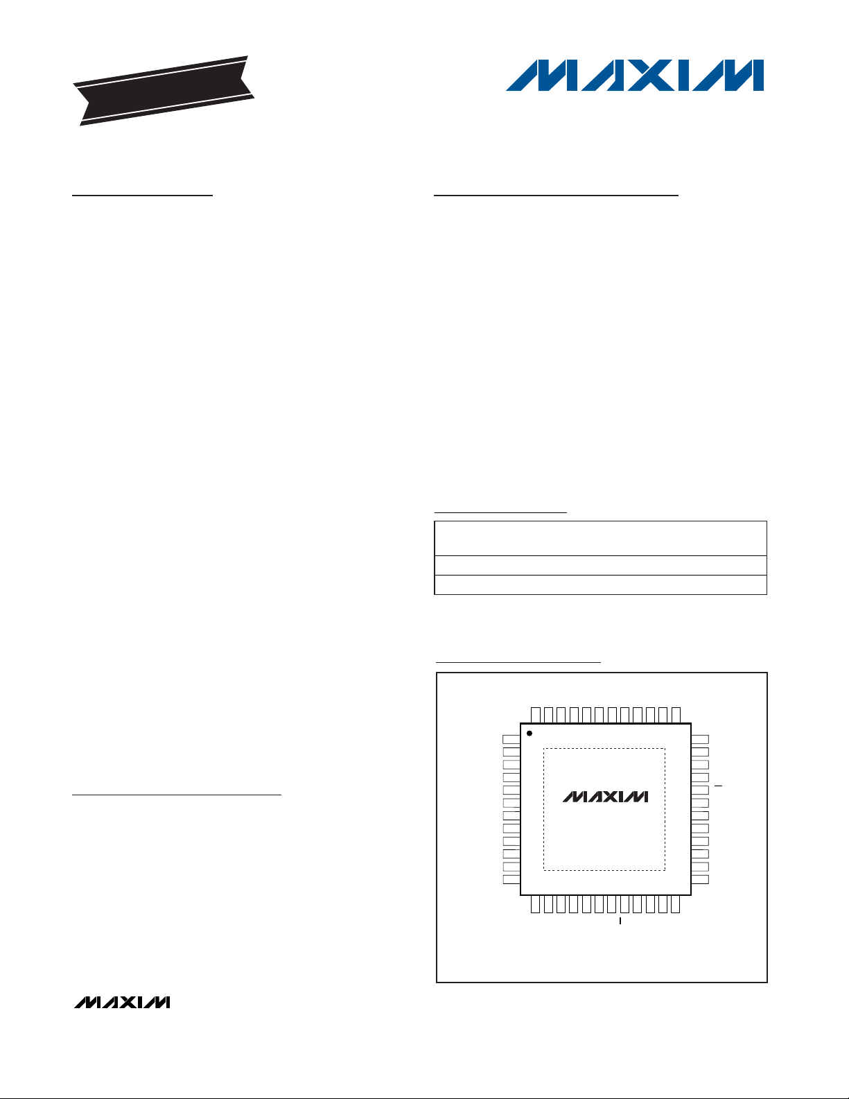
48 TQFP-EP
MAX1182
1314151617181920212223
24
4847464544434241403938
37
REFN
REFP
REFIN
REFOUT
D9A
D8A
D7A
D6A
D5A
D4A
D3A
D2A
EP
NOTE: THE PIN 1 INDICATOR FOR LEAD-FREE
PACKAGES IS REPLACED BY A "+" SIGN.
GND
V
DD
V
DD
GND
T/B
SLEEP
PD
OE
D9B
D8B
D7B
D6B
Pin Configuration
19-2094; Rev 1; 4/06
EVALUATION KIT
AVAILABLE
Ordering Information
PART
TEMP RANGE
PINPACKAGE
PKG
+Denotes lead-free package.
*EP = Exposed paddle.
Pin-Compatible Versions table at end of data sheet.
For pricing, delivery, and ordering information, please contact Maxim Direct at 1-888-629-4642,
or visit Maxim's website at www.maxim-ic.com.
MAX1182ECM -40°C to +85°C 48 TQFP-EP* C48E-7
M AX 1182E C M + -40°C to +85°C 48 TQFP-EP* C48E-7
CODE
MAX1182
Dual 10-Bit, 65Msps, 3V, Low-Power ADC
with Internal Reference and Parallel Outputs
2 _______________________________________________________________________________________
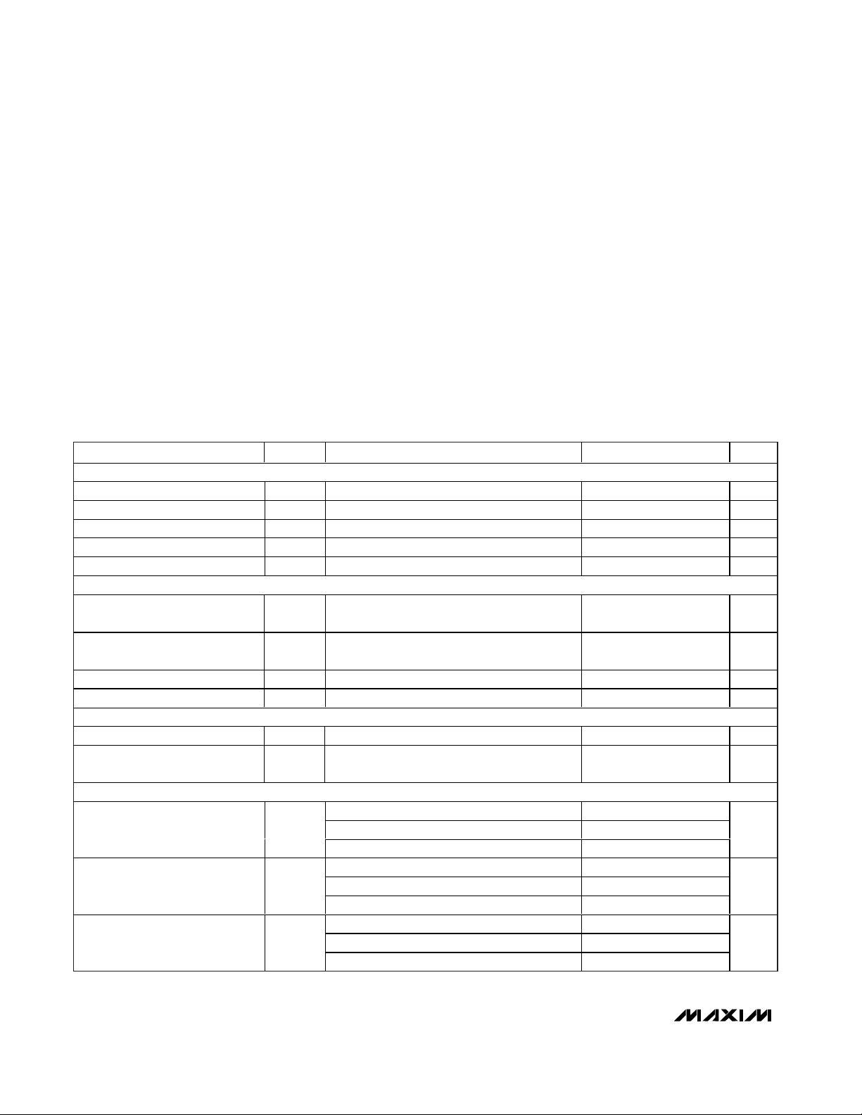
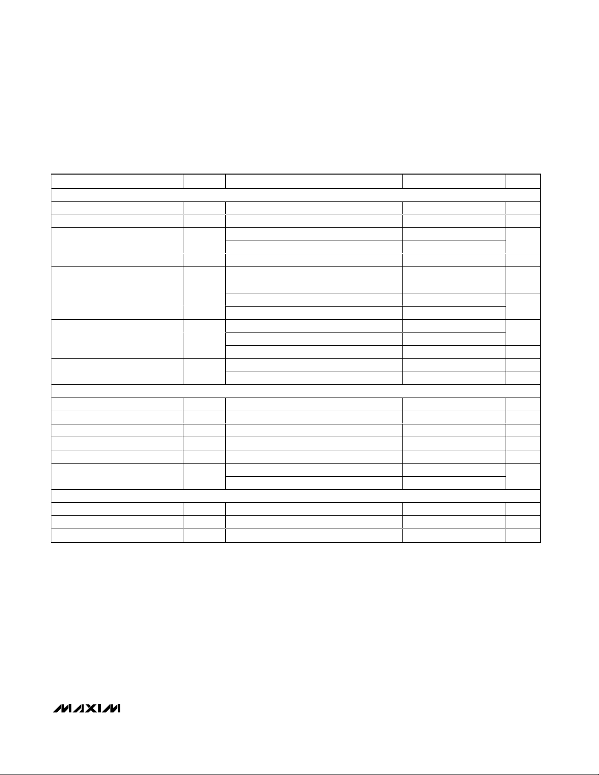
ABSOLUTE MAXIMUM RATINGS
ELECTRICAL CHARACTERISTICS
(VDD= 3V, OVDD= 2.5V; 0.1µF and 1.0µF capacitors from REFP, REFN, and COM to GND; REFOUT connected to REFIN through a
10kΩ resistor, V
IN
= 2Vp-p (differential w.r.t. COM), CL= 10pF at digital outputs (Note 1), f
CLK
= 65MHz (50% duty cycle),
T
A
= T
MIN
to T
MAX
, unless otherwise noted. Typical values are at TA= +25°C.) (Note 2)
Stresses beyond those listed under “Absolute Maximum Ratings” may cause permanent damage to the device. These are stress ratings only, and functional
operation of the device at these or any other conditions beyond those indicated in the operational sections of the specifications is not implied. Exposure to
absolute maximum rating conditions for extended periods may affect device reliability.
VDD, OVDD to GND...............................................-0.3V to +3.6V
OGND to GND.......................................................-0.3V to +0.3V
INA+, INA-, INB+, INB- to GND ...............................-0.3V to V
DD
REFIN, REFOUT, REFP, REFN, CLK,
COM to GND ..........................................-0.3V to (V
DD
+ 0.3V)
OE, PD, SLEEP, T/B, D9A–D0A,
D9B–D0B to OGND .............................-0.3V to (OV
DD
+ 0.3V)
Continuous Power Dissipation (T
A
= +70°C)
48-Pin TQFP-EP (derate 30.4mW/°C
above +70°C)............................................................2430mW
Operating Temperature Range ...........................-40°C to +85°C
Junction Temperature......................................................+150°C
Storage Temperature Range .............................-60°C to +150°C
Lead temperature (soldering, 10s) ..................................+300°C
PARAMETER
CONDITIONS
UNITS
DC ACCURACY
Resolution 10 Bits
Integral Nonlinearity INL fIN = 7.47MHz
LSB
Differential Nonlinearity DNL
LSB
Offset Error
% FS
Gain Error 0 ±2
% FS
ANALOG INPUT
Differential Input Voltage
Range
V
DIFF
Differential or single-ended inputs
V
Common-Mode Input Voltage
Range
V
CM
V
D D
/ 2
V
Input Resistance R
IN
Switched capacitor load 33 kΩ
Input Capacitance C
IN
5pF
CONVERSION RATE
Maximum Clock Frequency f
CLK
65
MHz
Data Latency 5
Clock
cycles
DYNAMIC CHARACTERISTICS
f
INA or B
= 7.47MHz, TA = +25°C
f
INA or B
= 20MHz, TA = +25°C
59
Signal-to-Noise Ratio
(Note 3)
SNR
f
INA or B
= 39.9MHz 59
dB
f
INA or B
= 7.47MHz, TA = +25°C
59
f
INA or B
= 20MHz, TA = +25°C56
Signal-to-Noise and Distortion
(Up to 5th Harmonic) (Note 3)
f
INA or B
= 39.9MHz
dB
f
INA or B
= 7.47MHz, TA = +25°C6576
f
INA or B
= 20MHz, TA = +25°C6577
Spurious-Free Dynamic Range
(Note 3)
SFDR
f
INA or B
= 39.9MHz 75
dBc
SYMBOL
fIN = 7.47MHz, no missing codes guaranteed ±0.4 ±1.0
MIN TYP MAX
±0.6 ±2.2
< ±1 ±1.7
SINAD
±1.0
± 0.5
56.8 59.5
56.5
56.5
58.5
58.5
MAX1182
Dual 10-Bit, 65Msps, 3V, Low-Power ADC
with Internal Reference and Parallel Outputs
_______________________________________________________________________________________ 3
ELECTRICAL CHARACTERISTICS (continued)
(VDD= 3V, OVDD= 2.5V; 0.1µF and 1.0µF capacitors from REFP, REFN, and COM to GND; REFOUT connected to REFIN through a
10kΩ resistor, V
IN
= 2Vp-p (differential w.r.t. COM), CL= 10pF at digital outputs (Note 1), f
CLK
= 65MHz (50% duty cycle),
T
A
= T
MIN
to T
MAX
, unless otherwise noted. Typical values are at TA= +25°C.) (Note 2)
PARAMETER
CONDITIONS
UNITS
f
INA or B
= 7.47MHz, TA = +25°C
-64
f
INA or B
= 20MHz, TA = +25°C -76 -63
Total Harmonic Distortion
(First 4 Harmonics) (Note 3)
THD
f
INA or B
= 39.9MHz -74
dBc
f
INA or B
= 7.47MHz -83
f
INA or B
= 20MHz -82
Third-Harmonic Distortion
(Note 3)
HD3
f
INA or B
= 39.9MHz -77
dBc
Intermodulation Distortion IMD
f
INA or B
= 19.13042MHz at -6.5dBFS
f
I N A o r B
= 21.2886M H z at - 6.5d BFS ( N ote 4)
-75
dBc
Small-Signal Bandwidth Input at -20dB FS, differential inputs
MHz
Full-Power Bandwidth
Input at -0.5dB FS, differential inputs
MHz
Aperture Delay t
AD
1ns
Aperture Jitter t
AJ
2
ps
RMS
Overdrive Recovery Time For 1.5x full-scale input 2 ns
Differential Gain ±1%
Differential Phase
d egr ees
Output Noise INA+ = INA- = INB+ = INB- = COM 0.2
LSB
RMS
INTERNAL REFERENCE
Reference Output Voltage
V
Reference Temperature
Coefficient
60
ppm/°C
Load Regulation
mV/mA
BUFFERED EXTERNAL REFERENCE (V
REFIN
= 2.048V)
REFIN Input Voltage
V
Positive Reference Output
Voltage
V
Negative Reference Output
Voltage
V
Differential Reference Output
Voltage Range
ΔV
REF
= V
REFP
- V
REFN
V
REFIN Resistance
MΩ
SYMBOL
FPBW
REFOUT
TC
REF
V
REFIN
V
REFP
V
REFN
ΔV
REF
R
REFIN
MIN TYP MAX
-75.5
500
400
±0.25
2.048
±3%
1.25
0.95 1.024 1.10
2.048
2.012
0.988
> 50
MAX1182
Dual 10-Bit, 65Msps, 3V, Low-Power ADC
with Internal Reference and Parallel Outputs
4 _______________________________________________________________________________________
ELECTRICAL CHARACTERISTICS (continued)
(VDD= 3V, OVDD= 2.5V; 0.1µF and 1.0µF capacitors from REFP, REFN, and COM to GND; REFOUT connected to REFIN through a
10kΩ resistor, V
IN
= 2Vp-p (differential w.r.t. COM), CL= 10pF at digital outputs (Note 1), f
CLK
= 65MHz (50% duty cycle),
T
A
= T
MIN
to T
MAX
, unless otherwise noted. Typical values are at TA= +25°C.) (Note 2)
PARAMETER
CONDITIONS
UNITS
Maximum REFP, COM Source
Current
> 5
mA
Maximum REFP, COM Sink
Current
I
SINK
µA
Maximum REFN Source Current
µA
Maximum REFN Sink Current I
SINK
> 5
mA
UNBUFFERED EXTERNAL REFERENCE (V
REFIN
= AGND, reference voltage applied to REFP, REFN, and COM)
REFP, REFN Input Resistance
R
REFP
,
Measured between REFP and COM, and
REFN and COM
4kΩ
Differential Reference Input
Voltage
ΔV
REF
= V
REFP
- V
REFN
V
COM Input Voltage V
COM
VDD / 2
V
REFP Input Voltage
V
COM
+
ΔV
REF
/ 2
V
REFN Input Voltage
V
COM
-
ΔV
REF
/ 2
V
DIGITAL INPUTS (CLK, PD, OE, SLEEP, T/B)
CLK
0.8
Input High Threshold V
IH
PD, OE, SLEEP, T/B
0.8
V
CLK
0.2
Input Low Threshold V
IL
PD, OE, SLEEP, T/B
0.2
V
Input Hysteresis
0.1 V
I
IH
VIH = OV
DD
or V
DD
(CLK) ±5
Input Leakage
I
IL
VIL = 0 ±5
µA
Input Capacitance C
IN
5pF
DIGITAL OUTPUTS (D9A–D0A, D9B–D0B)
Output-Voltage Low V
OL
I
SINK
= 200µA 0.2 V
Output-Voltage High V
OH
I
SOURCE
= 200µA
- 0.2
V
Three-State Leakage Current I
LEAK
OE = OV
DD
±10 µA
Three-State Output Capacitance
C
OUT
OE = OV
DD
5pF
SYMBOL
I
SOURCE
MIN TYP MAX
I
SOURCE
R
REFN
ΔV
REF
V
REFP
V
REFN
V
HYST
x V
DD
x OV
DD
250
250
1.024
±10%
± 10%
x V
x OV
DD
DD
OV
DD
MAX1182
Dual 10-Bit, 65Msps, 3V, Low-Power ADC
with Internal Reference and Parallel Outputs
_______________________________________________________________________________________ 5
ELECTRICAL CHARACTERISTICS (continued)
(VDD= 3V, OVDD= 2.5V; 0.1µF and 1.0µF capacitors from REFP, REFN, and COM to GND; REFOUT connected to REFIN through a
10kΩ resistor, V
IN
= 2Vp-p (differential w.r.t. COM), CL= 10pF at digital outputs (Note 1), f
CLK
= 65MHz (50% duty cycle),
T
A
= T
MIN
to T
MAX
, unless otherwise noted. Typical values are at TA= +25°C.) (Note 2)
PARAMETER
CONDITIONS
POWER REQUIREMENTS
Analog Supply Voltage Range V
DD
2.7 3.0 3.6 V
Output Supply Voltage Range OV
DD
1.7 2.5 3.6 V
Operating, f
INA or B
= 20MHz at -0.5dBFS 65 80
Sleep mode 2.8
mA
Analog Supply Current I
VDD
Shutdown, clock idle, PD = OE = OV
DD
115µA
Operating, CL = 15pF,
f
INA or B
= 20MHz at -0.5dBFS
11 mA
Sleep mode
Output Supply Current
Shutdown, clock idle, PD = OE = OV
DD
210
µA
Operating, f
INA or B
= 20MHz at -0.5dBFS
Sleep mode 8.4
Power Dissipation
Shutdown, clock idle, PD = OE = OV
DD
345µW
Offset
Power-Supply Rejection Ratio PSRR
Gain
TIMING CHARACTERISTICS
CLK Rise to Output Data Valid t
DO
Figure 3 (Note 5) 5 8 ns
Output Enable Time
Figure 4 10 ns
Output Disable Time
Figure 4 1.5 ns
CLK Pulse Width High t
CH
Figure 3, clock period: 15.4ns
7.7 ± 1.5
ns
CLK Pulse Width Low t
CL
Figure 3, clock period: 15.4ns
7.7 ± 1.5
ns
Wake-up from sleep mode (Note 6)
Wake-Up Time
Wake-up from shutdown (Note 6) 1.5
µs
CHANNEL-TO-CHANNEL MATCHING
Crosstalk f
INA or B
= 20MHz at -0.5dBFS -70 dB
Gain Matching f
INA or B
= 20MHz at -0.5dBFS
dB
Phase Matching f
INA or B
= 20MHz at -0.5dBFS
Note 1: Equivalent dynamic performance is obtainable over full OVDDrange with reduced CL.
Note 2: Specifications at ≥ +25°C are guaranteed by production test and < +25°C are guaranteed by design and characterization.
Note 3: SNR, SINAD, THD, SFDR, and HD3 are based on an analog input voltage of -0.5dBFS referenced to a ±1.024V full-scale
input voltage range.
Note 4: Intermodulation distortion is the total power of the intermodulation products relative to the individual carrier. This number is
6dB or better, if referenced to the two-tone envelope.
Note 5: Digital outputs settle to V
IH
, VIL. Parameter guaranteed by design.
Note 6: With REFIN driven externally, REFP, COM, and REFN are left floating while powered down.
SYMBOL
I
OVDD
PDISS
t
ENABLE
t
DISABLE
t
WAKE
MIN TYP MAX UNITS
100
195 240
±0.2 mV/V
±0.1 %/V
0.42
0.02 ±0.2
0.25 d eg r ees
mW
MAX1182
Dual 10-Bit, 65Msps, 3V, Low-Power ADC
with Internal Reference and Parallel Outputs
6 _______________________________________________________________________________________
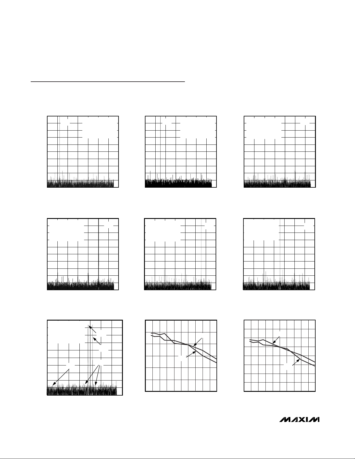
Typical Operating Characteristics
(VDD= 3V, OVDD= 2.5V, internal reference, differential input at -0.5dBFS, f
CLK
= 65MHz, CL≈ 10pF, TA= +25°C, unless otherwise
noted.)
-100
-70
-80
-90
-50
-60
-10
-20
-30
-40
0
0 5 10 15 20 25 30 35
FFT PLOT CHA (8192-POINT RECORD,
DIFFERENTIAL INPUT)
MAX1182 toc01
ANALOG INPUT FREQUENCY (MHz)
AMPLITUDE (dB)
CHA
f
INA
= 6.0065MHz
f
INB
= 7.51410MHz
f
CLK
= 65.00057MHz
A
INA
= -0.55dBFS
-100
-70
-80
-90
-50
-60
-10
-20
-30
-40
0
0 5 10 15 20 25 30 35
FFT PLOT CHB (8192-POINT RECORD,
DIFFERENTIAL INPUT)
MAX1182 toc02
ANALOG INPUT FREQUENCY (MHz)
AMPLITUDE (dB)
CHB
f
INA
= 6.0065MHz
f
INB
= 7.51410MHz
f
CLK
= 65.00057MHz
A
INB
= -0.56dBFS
-100
-70
-80
-90
-50
-60
-10
-20
-30
-40
0
0 5 10 15 20 25 30 35
FFT PLOT CHA (8192-POINT RECORD,
DIFFERENTIAL INPUT)
MAX1182 toc03
ANALOG INPUT FREQUENCY (MHz)
AMPLITUDE (dB)
CHA
f
INA
= 20.08257MHz
f
INB
= 25.09727MHz
f
CLK
= 65.00057MHz
A
INB
= -0.52dBFS
-100
-70
-80
-90
-50
-60
-10
-20
-30
-40
0
0 5 10 15 20 25 30 35
FFT PLOT CHB (8192-POINT RECORD,
DIFFERENTIAL INPUT)
MAX1182 toc04
ANALOG INPUT FREQUENCY (MHz)
AMPLITUDE (dB)
CHB
f
INA
= 20.08257MHz
f
INB
= 25.09727MHz
f
CLK
= 65.00057MHz
A
INB
= -0.52dBFS
-100
-70
-80
-90
-50
-60
-10
-20
-30
-40
0
0 5 10 15 20 25 30 35
FFT PLOT CHA (8192-POINT RECORD,
DIFFERENTIAL INPUT)
MAX1182 toc05
ANALOG INPUT FREQUENCY (MHz)
AMPLITUDE (dB)
CHA
f
INA
= 37.31661MHz
f
INB
= 46.99687MHz
f
CLK
= 65.00057MHz
A
INB
= -0.52dBFS
-100
-70
-80
-90
-50
-60
-10
-20
-30
-40
0
0 5 10 15 20 25 30 35
FFT PLOT CHB (8192-POINT RECORD,
DIFFERENTIAL INPUT)
MAX1182 toc06
ANALOG INPUT FREQUENCY (MHz)
AMPLITUDE (dB)
CHB
f
INA
= 37.31661MHz
f
INB
= 46.99687MHz
f
CLK
= 65.00057MHz
A
INB
= -0.49dBFS
-100
-70
-80
-90
-50
-60
-10
-20
-30
-40
0
0 5 10 15 20 25 30 35
TWO-TONE IMD PLOT (8192-POINT RECORD,
DIFFERENTIAL INPUT)
MAX1182 toc07
ANALOG INPUT FREQUENCY (MHz)
AMPLITUDE (dB)
f
IN1
f
IN1
= 19.13042MHz
f
IN2
= 21.28864MHz
f
CLK
= 65.00057MHz
A
IN
= -6.5dBFS
f
IN2
IM2
IM3
SIGNAL-TO-NOISE RATIO
vs. ANALOG INPUT FREQUENCY
MAX1182 toc08
ANALOG INPUT FREQUENCY (MHz)
SNR (dB)
61
55
56
57
58
59
60
0 102030405060708090100
CHA
CHB
62
61
54
010 2030405060708090100
56
55
58
57
59
60
SIGNAL-TO-NOISE AND DISTORTION
vs. ANALOG INPUT FREQUENCY
MAX1182 toc09
ANALOG INPUT FREQUENCY (MHz)
SINAD (dB)
CHA
CHB
MAX1182
Dual 10-Bit, 65Msps, 3V, Low-Power ADC
with Internal Reference and Parallel Outputs
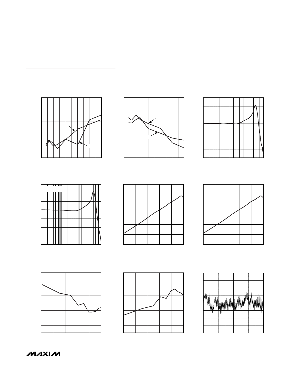
_______________________________________________________________________________________ 7
-60
-80
0
10
20
30 40 50 60 70 80 90 100
TOTAL HARMONIC DISTORTION
vs. ANALOG INPUT FREQUENCY
-76
MAX1182 toc10
ANALOG INPUT FREQUENCY (MHz)
THD (dBc)
-72
-68
-64
CHB
CHA
0 10 20 30 40 50 60 70 80 90 100
SPURIOUS-FREE DYNAMIC RANGE
vs. ANALOG INPUT FREQUENCY
MAX1182 toc11
ANALOG INPUT FREQUENCY (MHz)
SFDR (dBc)
63
67
71
75
79
83
87
CHB
CHA
-8
-4
-6
0
-2
4
2
6
FULL-POWER INPUT BANDWIDTH
vs. ANALOG INPUT FREQUENCY, SINGLE-ENDED
MAX1182 toc12
ANALOG INPUT FREQUENCY (MHz)
GAIN (dB)
1 100 100010
-8
-4
-6
0
-2
4
2
6
SMALL-SIGNAL INPUT BANDWIDTH
vs. ANALOG INPUT FREQUENCY, SINGLE-ENDED
MAX1182 toc13
ANALOG INPUT FREQUENCY (MHz)
GAIN (dB)
1 100 100010
AIN = 100mV
P-P
35
45
40
55
50
60
65
-20 -12-16 -8 -4 0
SIGNAL-TO-NOISE RATIO
vs. ANALOG INPUT POWER (f
IN
= 20.09MHz)
MAX1182 toc14
ANALOG INPUT POWER (dBFS)
SNR (dB)
35
45
40
55
50
60
65
-20 -12-16 -8 -4 0
SIGNAL-TO-NOISE + DISTORTION
vs. ANALOG INPUT POWER (f
IN
= 20.09MHz)
MAX1182 toc15
ANALOG INPUT POWER (dBFS)
SINAD (dB)
-20 -12-16 -8 -4 0
TOTAL HARMONIC DISTORTION
vs. ANALOG INPUT POWER (f
IN
= 20.09MHz)
MAX1182 toc16
ANALOG INPUT POWER (dBFS)
THD (dB)
-90
-85
-65
-70
-75
-80
-60
-50
-55
-20 -12-16 -8 -4 0
SPURIOUS-FREE DYNAMIC RANGE
vs. ANALOG INPUT POWER (f
IN
= 20.09MHz)
MAX1182 toc17
ANALOG INPUT POWER (dBFS)
SFDR (dB)
50
55
75
70
65
60
85
80
90
-1.00
-0.50
-0.75
0.50
0.25
0
-0.25
1.00
0.75
0 256 384128 512 640 768 896 1024
INTEGRAL NONLINEARITY
(BEST-ENDPOINT FIT)
MAX1182 toc18
DIGITAL OUTPUT CODE
INL (LSB)
Typical Operating Characteristics (continued)
(VDD= 3V, OVDD= 2.5V, internal reference, differential input at -0.5dBFS, f
CLK
= 65MHz, CL≈ 10pF, TA= +25°C, unless otherwise
noted.)

MAX1182
Dual 10-Bit, 65Msps, 3V, Low-Power ADC
with Internal Reference and Parallel Outputs
8 _______________________________________________________________________________________
-0.5
-0.3
-0.4
-0.1
-0.2
0.1
0
0.2
0.4
0.3
0.5
0 256 384128 512 640 768 896 1024
DIFFERENTIAL NONLINEARITY
MAX1182 toc19
DIGITAL OUTPUT CODE
DNL (LSB)
-3.0
-2.5
-2.0
-1.5
-1.0
-0.5
0
0.5
1.0
-40 -15 10 35 60 85
GAIN ERROR vs. TEMPERATURE,
EXTERNAL REFERENCE (V
REFIN
= 2.048V)
MAX1182 toc20
TEMPERATURE (°C)
GAIN ERROR (% FS)
CHB
CHA
-0.15
-0.05
-0.10
0.05
0
0.10
0.15
-40 10-15 35 60 85
OFFSET ERROR vs. TEMPERATURE,
EXTERNAL REFERENCE
(V
REFIN
= 2.048V)
MAX1182 toc21
TEMPERATURE (°C)
OFFSET ERROR (% FS)
CHB
CHA
80
70
60
50
40
2.70 3.152.85 3.00 3.30 3.45 3.60
ANALOG SUPPLY CURRENT
vs. ANALOG SUPPLY VOLTAGE
MAX1182 toc22
VDD (V)
I
VDD
(mA)
85
75
65
55
45
ANALOG SUPPLY CURRENT
vs. TEMPERATURE
MAX1182 toc23
TEMPERATURE (°C)
I
VDD
(mA)
-40 10-15 35 60 85
0
0.06
0.18
0.12
0.24
0.30
2.70 3.002.85 3.15 3.30 3.45 3.60
ANALOG POWER-DOWN CURRENT
vs. ANALOG SUPPLY VOLTAGE
MAX1182 toc24
VDD (V)
I
VDD
(μA)
OE = PD = OV
DD
40
50
70
60
80
90
30 40 4535 50 55 60 65 70
SNR/SINAD, -THD/SFDR
vs. CLOCK DUTY CYCLE
MAX1182 toc25
CLOCK DUTY CYCLE (%)
SNR/SINAD, -THD/SFDR (dB, dBc)
SFDR
SNR
-THD
SINAD
fIN = 25.097265MHz
2.020
2.025
2.035
2.030
2.040
2.045
2.70 3.002.85 3.15 3.30 3.45 3.60
INTERNAL REFERENCE VOLTAGE
vs. ANALOG SUPPLY VOLTAGE
MAX1182 toc26
VDD (V)
V
REFOUT
(V)
Typical Operating Characteristics (continued)
(VDD= 3V, OVDD= 2.5V, internal reference, differential input at -0.5dBFS, f
CLK
= 65MHz, CL≈ 10pF, TA= +25°C, unless otherwise
noted.)

MAX1182
Dual 10-Bit, 65Msps, 3V, Low-Power ADC
with Internal Reference and Parallel Outputs
_______________________________________________________________________________________ 9
2.00
2.02
2.01
2.04
2.03
2.05
2.06
-40 10-15 35 60 85
INTERNAL REFERENCE VOLTAGE
vs. TEMPERATURE
MAX1182 toc27
TEMPERATURE (°C)
V
REFOUT
(V)
0
20000
40000
60000
80000
100000
120000
140000
160000
N-2 N-1 N N+1 N+2
OUTPUT NOISE HISTOGRAM (DC INPUT)
MAX1182 toc28
DIGITAL OUTPUT CODE
COUNTS
0
926
129421
725
0
Typical Operating Characteristics (continued)
(VDD= 3V, OVDD= 2.5V, internal reference, differential input at -0.5dBFS, f
CLK
= 65MHz, CL≈ 10pF, TA= +25°C, unless otherwise
noted.)
Pin Description
PIN NAME FUNCTION
1 COM Common-Mode Voltage Input/Output. Bypass to GND with a ≥ 0.1µF capacitor.
2, 6, 11, 14, 15
V
DD
Analog Supply Voltage. Bypass each supply pin to GND with a 0.1µF capacitor. Analog
supply accepts a 2.7V to 3.6V input range.
3, 7, 10, 13, 16
GND Analog Ground
4 INA+ Channel A Positive Analog Input. For single-ended operation, connect signal source to INA+.
5 INA- Channel A Negative Analog Input. For single-ended operation, connect INA- to COM.
8 INB- Channel B Negative Analog Input. For single-ended operation, connect INB- to COM.
9 INB+ Channel B Positive Analog Input. For single-ended operation, connect signal source to INB+.
12 CLK Converter Clock Input
17 T/B
T/B selects the ADC digital output format.
High: Two’s complement.
Low: Straight offset binary.
18 SLEEP
Sleep Mode Input.
High: Deactivates the two ADCs, but leaves the reference bias circuit active.
Low: Normal operation.
19 PD
Power-Down Input.
High: Power-down mode
Low: Normal operation
20 OE
Output Enable Input.
High: Digital outputs disabled
Low: Digital outputs enabled

MAX1182
Dual 10-Bit, 65Msps, 3V, Low-Power ADC
with Internal Reference and Parallel Outputs
10 ______________________________________________________________________________________
Pin Description (continued)
PIN NAME FUNCTION
21 D9B Three-State Digital Output, Bit 9 (MSB), Channel B
22 D8B Three-State Digital Output, Bit 8, Channel B
23 D7B Three-State Digital Output, Bit 7, Channel B
24 D6B Three-State Digital Output, Bit 6, Channel B
25 D5B Three-State Digital Output, Bit 5, Channel B
26 D4B Three-State Digital Output, Bit 4, Channel B
27 D3B Three-State Digital Output, Bit 3, Channel B
28 D2B Three-State Digital Output, Bit 2, Channel B
29 D1B Three-State Digital Output, Bit 1, Channel B
30 D0B Three-State Digital Output, Bit 0 (LSB), Channel B
31, 34 OGND Output Driver Ground
32, 33 OV
DD
Output Driver Supply Voltage. Bypass each supply pin to OGND with a 0.1µF capacitor.
Output driver supply accepts a 1.7V to 3.6V input range.
35 D0A Three-State Digital Output, Bit 0 (LSB), Channel A
36 D1A Three-State Digital Output, Bit 1, Channel A
37 D2A Three-State Digital Output, Bit 2, Channel A
38 D3A Three-State Digital Output, Bit 3, Channel A
39 D4A Three-State Digital Output, Bit 4, Channel A
40 D5A Three-State Digital Output, Bit 5, Channel A
41 D6A Three-State Digital Output, Bit 6, Channel A
42 D7A Three-State Digital Output, Bit 7, Channel A
43 D8A Three-State Digital Output, Bit 8, Channel A
44 D9A Three-State Digital Output, Bit 9 (MSB), Channel A
45 REFOUT
Internal Reference Voltage Output. May be connected to REFIN through a resistor or a resistor
divider.
46 REFIN Reference Input. V
REFIN
= 2 x (V
REFP
- V
REFN
). Bypass to GND with a > 1nF capacitor.
47 REFP
Positive Reference Input/Output. Conversion range is ± (V
REFP
- V
REFN
). Bypass to GND with a
> 0.1µF capacitor.
48 REFN
Negative Reference Input/Output. Conversion range is ± (V
REFP
- V
REFN
). Bypass to GND with
a > 0.1µF capacitor.
— EP Exposed Paddle. Connect to analog ground.
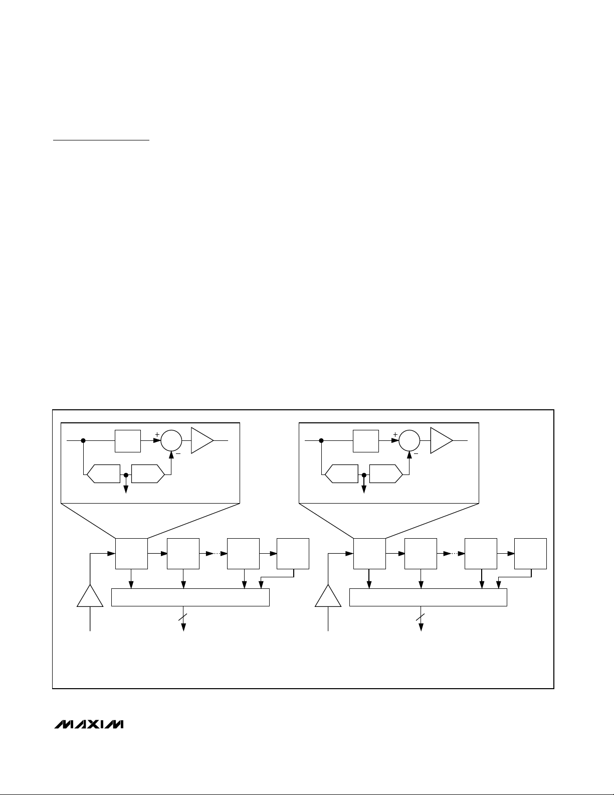
Detailed Description
The MAX1182 uses a 9-stage, fully-differential
pipelined architecture (Figure 1) that allows for highspeed conversion while minimizing power consumption. Samples taken at the inputs move progressively
through the pipeline stages every half clock cycle.
Counting the delay through the output latch, the clockcycle latency is five clock cycles.
1.5-bit (2-comparator) flash ADCs convert the heldinput voltages into a digital code. The digital-to-analog
converters (DACs) convert the digitized results back
into analog voltages, which are then subtracted from
the original held input signals. The resulting error signals are then multiplied by two and the residues are
passed along to the next pipeline stages where the
process is repeated until the signals have been
processed by all nine stages. Digital error correction
compensates for ADC comparator offsets in each of
these pipeline stages and ensures no missing codes.
Input Track-and-Hold (T/H) Circuits
Figure 2 displays a simplified functional diagram of the
input track-and-hold (T/H) circuits in both track and
hold mode. In track mode, switches S1, S2a, S2b, S4a,
S4b, S5a and S5b are closed. The fully-differential circuits sample the input signals onto the two capacitors
(C2a and C2b) through switches S4a and S4b. S2a and
S2b set the common mode for the amplifier input, and
open simultaneously with S1, sampling the input waveform. Switches S4a and S4b are then opened before
switches S3a and S3b, connect capacitors C1a and
C1b to the output of the amplifier, and switch S4c is
closed. The resulting differential voltages are held on
capacitors C2a and C2b. The amplifiers are used to
charge capacitors C1a and C1b to the same values
originally held on C2a and C2b. These values are then
presented to the first-stage quantizers and isolate the
pipelines from the fast-changing inputs. The wide input
bandwidth T/H amplifiers allow the MAX1182 to trackand-sample/hold analog inputs of high frequencies (>
Nyquist). The ADC inputs (INA+, INB+, INA-, and INB-)
can be driven either differentially or single-ended.
Match the impedance of INA+ and INA- as well as
INB+ and INB- and set the common-mode voltage to
mid-supply (V
DD
/ 2) for optimum performance.
MAX1182
Dual 10-Bit, 65Msps, 3V, Low-Power ADC
with Internal Reference and Parallel Outputs
______________________________________________________________________________________ 11
V
INA
= INPUT VOLTAGE BETWEEN INA+ AND INA- (DIFFERENTIAL OR SINGLE-ENDED)
V
INB
= INPUT VOLTAGE BETWEEN INB+ AND INB- (DIFFERENTIAL OR SINGLE-ENDED)
T/H
V
OUT
x2
Σ
FLASH
ADC
DAC
1.5 BITS
10
V
INA
V
IN
STAGE 1 STAGE 2
D9A–D0A
DIGITAL CORRECTION LOGIC
STAGE 8 STAGE 9
2-BIT FLASH
ADC
T/H
T/H
V
OUT
x2
Σ
FLASH
ADC
DAC
1.5 BITS
10
V
INB
V
IN
STAGE 1 STAGE 2
D9B–D0B
DIGITAL CORRECTION LOGIC
STAGE 8 STAGE 9
2-BIT FLASH
ADC
T/H
Figure 1. Pipelined Architecture—Stage Blocks

MAX1182
Dual 10-Bit, 65Msps, 3V, Low-Power ADC
with Internal Reference and Parallel Outputs
12 ______________________________________________________________________________________
S3b
S3a
COM
S5b
S5a
INB+
INB-
S1
OUT
OUT
C2a
C2b
S4c
S4a
S4b
C1b
C1a
INTERNAL
BIAS
INTERNAL
BIAS
COM
HOLD
HOLD
CLK
INTERNAL
NONOVERLAPPING
CLOCK SIGNALS
TRACK
TRACK
S2a
S2b
S3b
S3a
COM
S5b
S5a
INA+
INA-
S1
OUT
OUT
C2a
C2b
S4c
S4a
S4b
C1b
C1a
INTERNAL
BIAS
INTERNAL
BIAS
COM
S2a
S2b
MAX1182
Figure 2. MAX1182 T/H Amplifiers

MAX1182
Dual 10-Bit, 65Msps, 3V, Low-Power ADC
with Internal Reference and Parallel Outputs
______________________________________________________________________________________ 13
Analog Inputs and Reference
Configurations
The full-scale range of the MAX1182 is determined by the
internally generated voltage difference between REFP
(V
DD
/ 2 + V
REFIN
/ 4) and REFN (V
DD
/ 2 - V
REFIN
/ 4).
The full-scale range for both on-chip ADCs is adjustable
through the REFIN pin, which is provided for this purpose.
REFOUT, REFP, COM (VDD/ 2), and REFN are internally buffered low-impedance outputs.
The MAX1182 provides three modes of reference operation:
• Internal reference mode
• Buffered external reference mode
• Unbuffered external reference mode
In internal reference mode, connect the internal reference output REFOUT to REFIN through a resistor (e.g.,
10kΩ) or resistor divider, if an application requires a
reduced full-scale range. For stability and noise filtering
purposes bypass REFIN with a > 10nF capacitor to
GND. In internal reference mode, REFOUT, COM,
REFP, and REFN become low-impedance outputs.
In buffered external reference mode, adjust the reference voltage levels externally by applying a stable and
accurate voltage at REFIN. In this mode, COM, REFP,
and REFN become outputs. REFOUT may be left open
or connected to REFIN through a > 10kΩ resistor.
In unbuffered external reference mode, connect REFIN
to GND. This deactivates the on-chip reference buffers
for REFP, COM, and REFN. With their buffers shut
down, these nodes become high impedance and may
be driven through separate external reference sources.
Clock Input (CLK)
The MAX1182’s CLK input accepts CMOS-compatible
clock signals. Since the interstage conversion of the
device depends on the repeatability of the rising and
falling edges of the external clock, use a clock with low
jitter and fast rise and fall times (< 2ns). In particular,
sampling occurs on the rising edge of the clock signal,
requiring this edge to provide lowest possible jitter. Any
significant aperture jitter would limit the SNR performance of the on-chip ADCs as follows:
SNR
dB
= 20 ✕log10(1 / [2π x fINx tAJ]),
where fINrepresents the analog input frequency and t
AJ
is the time of the aperture jitter.
Clock jitter is especially critical for undersampling
applications. The clock input should always be consid-
ered as an analog input and routed away from any analog input or other digital signal lines.
The MAX1182 clock input operates with a voltage threshold set to V
DD
/ 2. Clock inputs with a duty cycle other
than 50%, must meet the specifications for high and low
periods as stated in the Electrical Characteristics.
System Timing Requirements
Figure 3 depicts the relationship between the clock
input, analog input, and data output. The MAX1182
samples at the rising edge of the input clock. Output
data for channels A and B is valid on the next rising
edge of the input clock. The output data has an internal
latency of five clock cycles. Figure 4 also determines
the relationship between the input clock parameters
and the valid output data on channels A and B.
Digital Output Data, Output Data Format
Selection (T/B), Output Enable (/OE)
All digital outputs, D0A–D9A (Channel A) and D0B–D9B
(Channel B), are TTL/CMOS logic-compatible. There is
a 5-clock-cycle latency between any particular sample
and its corresponding output data. The output coding
can be chosen to be either straight offset binary or
two’s complement (Table 1) controlled by a single pin
(T/B). Pull T/B low to select offset binary and high to
activate two’s complement output coding. The capacitive load on the digital outputs D0A–D9A and D0B–D9B
should be kept as low as possible (< 15pF), to avoid
large digital currents that could feed back into the analog portion of the MAX1182, thereby degrading its
dynamic performance. Using buffers on the digital outputs of the ADCs can further isolate the digital outputs
from heavy capacitive loads. To further improve the
dynamic performance of the MAX1182 small-series
resistors (e.g., 100Ω) maybe added to the digital output
paths, close to the MAX1182.
Figure 4 displays the timing relationship between output enable and data output valid as well as power
down/wake-up and data output valid.
Power-Down (PD) and
Sleep (SLEEP) Modes
The MAX1182 offers two power-save modes—sleep and
full power-down mode. In sleep mode (SLEEP = 1), only
the reference bias circuit is active (both ADCs are disabled), and current consumption is reduced to 2.8mA.
To enter full power-down mode, pull PD high. With OE
simultaneously low, all outputs are latched at the last
value prior to the power down. Pulling OE high forces
the digital outputs into a high impedance state.

MAX1182
Dual 10-Bit, 65Msps, 3V, Low-Power ADC
with Internal Reference and Parallel Outputs
14 ______________________________________________________________________________________
Applications Information
Figure 5 depicts a typical application circuit containing
two single-ended to differential converters. The internal
reference provides a V
DD
/ 2 output voltage for level
shifting purposes. The input is buffered and then split to
a voltage follower and inverter. One lowpass filter per
ADC suppresses some of the wideband noise associated with high-speed operational amplifiers, follows the
amplifiers. The user may select the R
ISO
and CINvalues to optimize the filter performance, to suit a particular application. For the application in Figure 5, a R
ISO
of
50Ω is placed before the capacitive load to prevent
ringing and oscillation. The 22pF CINcapacitor acts as
a small bypassing capacitor.
Using Transformer Coupling
A RF transformer (Figure 6) provides an excellent solution to convert a single-ended source signal to a fully
differential signal, required by the MAX1182 for optimum performance. Connecting the center tap of the
transformer to COM provides a V
DD
/ 2 DC level shift to
the input. Although a 1:1 transformer is shown, a stepup transformer may be selected to reduce the drive
requirements. A reduced signal swing from the input
driver, such as an op amp, may also improve the overall distortion.
In general, the MAX1182 provides better SFDR and
THD with fully-differential input signals than singleended drive, especially for very high input frequencies.
In differential input mode, even-order harmonics are
lower as both inputs (INA+, INA- and/or INB+, INB-) are
balanced, and each of the ADC inputs only requires
half the signal swing compared to single-ended mode.
N - 6
N
N - 5
N + 1
N - 4
N + 2
N - 3
N + 3
N - 2
N + 4
N - 1
N + 5
N
N + 6
N + 1
5 CLOCK-CYCLE LATENCY
ANALOG INPUT
CLOCK INPUT
DATA OUTPUT
D9A–D0A
t
D0
t
CH
t
CL
N - 6 N - 5 N - 4 N - 3 N - 2 N - 1 N N + 1
DATA OUTPUT
D9B–D0B
Figure 3. System Timing Diagram
Figure 4. Output Timing Diagram
OE
t
DISABLE
VALID DATA
VALID DATA
OUTPUT
D9A–D0A
OUTPUT
D9B–D0B
HIGH IMPEDANCE
HIGH IMPEDANCE
t
ENABLE
HIGH IMPEDANCE
HIGH IMPEDANCE
MAX1182
Dual 10-Bit, 65Msps, 3V, Low-Power ADC
with Internal Reference and Parallel Outputs
______________________________________________________________________________________ 15
Table 1. MAX1182 Output Codes For Differential Inputs
*V
REF
= V
REFP
- V
REFN
DIFFERENTIAL INPUT
VOLTAGE*
DIFFERENTIAL
INPUT
STRAIGHT OFFSET
BINARY
T/B = 0
TWO’S COMPLEMENT
T/B = 1
V
REF
x 511/512 +FULL SCALE - 1 LSB 11 1111 1111 01 1111 1111
V
REF
x 1/512 +1 LSB 10 0000 0001 00 0000 0001
0 Bipolar Zero 10 0000 0000 00 0000 0000
-V
REF
x 1/512 -1 LSB 01 1111 1111 11 1111 1111
-V
REF
x 511/512 -FULL SCALE + 1 LSB 00 0000 0001 10 0000 0001
-V
REF
x 512/512 -FULL SCALE 00 0000 0000 10 0000 0000
Single-Ended AC-Coupled Input Signal
Figure 7 shows an AC-coupled, single-ended application. Amplifiers like the MAX4108 provide high-speed,
high-bandwidth, low noise, and low distortion to maintain the integrity of the input signal.
Typical QAM Demodulation Application
The most frequently used modulation technique for digital communications applications is probably the
Quadrature Amplitude Modulation (QAM). Typically
found in spread-spectrum based systems, a QAM signal
represents a carrier frequency modulated in both amplitude and phase. At the transmitter, modulating the baseband signal with quadrature outputs, a local oscillator
followed by subsequent up-conversion can generate the
QAM signal. The result is an in-phase (I) and a quadrature (Q) carrier component, where the Q component is
90 degree phase-shifted with respect to the in-phase
component. At the receiver, the QAM signal is divided
down into it’s I and Q components, essentially representing the modulation process reversed. Figure 8 displays the demodulation process performed in the
analog domain, using the dual matched 3V, 10-bit ADC
MAX1182 and the MAX2451 quadrature demodulator to
recover and digitize the I and Q baseband signals.
Before being digitized by the MAX1182, the mixed-down
signal components may be filtered by matched analog
filters, such as Nyquist or pulse-shaping filters which
remove any unwanted images from the mixing process,
thereby enhancing the overall signal-to-noise (SNR) performance and minimizing inter-symbol interference.
Grounding, Bypassing, and
Board Layout
The MAX1182 requires high-speed board layout design
techniques. Locate all bypass capacitors as close to
the device as possible, preferably on the same side as
the ADC, using surface-mount devices for minimum
inductance. Bypass VDD, REFP, REFN, and COM with
two parallel 0.1µF ceramic capacitors and a 2.2µF
bipolar capacitor to GND. Follow the same rules to
bypass the digital supply (OVDD) to OGND. Multilayer
boards with separated ground and power planes produce the highest level of signal integrity. Consider the
use of a split ground plane arranged to match the
physical location of the analog ground (GND) and the
digital output driver ground (OGND) on the ADCs package. The two ground planes should be joined at a single point such that the noisy digital ground currents do
not interfere with the analog ground plane. The ideal
location of this connection can be determined experimentally at a point along the gap between the two
ground planes, which produces optimum results. Make
this connection with a low-value, surface-mount resistor
(1Ω to 5Ω), a ferrite bead or a direct short. Alternatively,
all ground pins could share the same ground plane, if
the ground plane is sufficiently isolated from any noisy,
digital systems ground plane (e.g., downstream output
buffer or DSP ground plane). Route high-speed digital
signal traces away from the sensitive analog traces of
either channel. Make sure to isolate the analog input
lines to each respective converter to minimize channelto-channel crosstalk. Keep all signal lines short and
free of 90 degree turns.
MAX1182
Dual 10-Bit, 65Msps, 3V, Low-Power ADC
with Internal Reference and Parallel Outputs
16 ______________________________________________________________________________________
Figure 5. Typical Application for Single-Ended-to-Differential Conversion
INPUT
300Ω
-5V
+5V
0.1μF
0.1μF
0.1μF
-5V
600Ω
300Ω
300Ω
INA+
INA-
LOWPASS FILTER
COM
600Ω
+5V
-5V
0.1μF
600Ω
300Ω
600Ω
300Ω
0.1μF
0.1μF
0.1μF
+5V
0.1μF
300Ω
MAX4108
MAX1182
INB+
INB-
MAX4108
MAX4108
LOWPASS FILTER
INPUT
300Ω
-5V
+5V
0.1μF
0.1μF
0.1μF
C
IN
22pF
-5V
600Ω
300Ω
300Ω
LOWPASS FILTER
600Ω
+5V
-5V
0.1μF
600Ω
300Ω
600Ω
300Ω
0.1μF
0.1μF
0.1μF
+5V
0.1μF
300Ω
MAX4108
MAX4108
MAX4108
LOWPASS FILTER
R
IS0
50Ω
C
IN
22pF
R
IS0
50Ω
C
IN
22pF
R
IS0
50Ω
C
IN
22pF
R
IS0
50Ω
MAX1182
Dual 10-Bit, 65Msps, 3V, Low-Power ADC
with Internal Reference and Parallel Outputs
______________________________________________________________________________________ 17
Figure 6. Transformer-Coupled Input Drive
MAX1182
T1
N.C.
V
IN
6
1
5
2
43
22pF
22pF
0.1μF
0.1μF
2.2μF
25Ω
25Ω
MINICIRCUITS
TT1–6
T1
N.C.
V
IN
6
1
5
2
4
3
22pF
22pF
0.1μF
0.1μF
2.2μF
25Ω
25Ω
MINICIRCUITS
TT1–6
INA-
INA+
INB-
INB+
COM
Static Parameter Definitions
Integral Nonlinearity (INL)
Integral nonlinearity is the deviation of the values on an
actual transfer function from a straight line. This straight
line can be either a best straight-line fit or a line drawn
between the endpoints of the transfer function, once
offset and gain errors have been nullified. The static linearity parameters for the MAX1182 are measured using
the best straight-line fit method.
Differential Nonlinearity (DNL)
Differential nonlinearity is the difference between an
actual step-width and the ideal value of 1 LSB. A DNL
error specification of less than 1 LSB guarantees no
missing codes and a monotonic transfer function.
Dynamic Parameter Definitions
Aperture Jitter
Figure 9 depicts the aperture jitter (tAJ), which is the
sample-to-sample variation in the aperture delay.
Aperture Delay
Aperture delay (tAD) is the time defined between the
falling edge of the sampling clock and the instant when
an actual sample is taken (Figure 9).
MAX1182
Dual 10-Bit, 65Msps, 3V, Low-Power ADC
with Internal Reference and Parallel Outputs
18 ______________________________________________________________________________________
Signal-to-Noise Ratio (SNR)
For a waveform perfectly reconstructed from digital
samples, the theoretical maximum SNR is the ratio of the
full-scale analog input (RMS value) to the RMS quantization error (residual error). The ideal, theoretical minimum
analog-to-digital noise is caused by quantization error
only and results directly from the ADC’s resolution
(N-Bits):
SNR
dB[max]
= 6.02 x N + 1.76
In reality, there are other noise sources besides quantization noise e.g. thermal noise, reference noise, clock
jitter, etc. SNR is computed by taking the ratio of the
RMS signal to the RMS noise, which includes all spectral components minus the fundamental, the first five
harmonics, and the DC offset.
Signal-to-Noise Plus Distortion (SINAD)
SINAD is computed by taking the ratio of the RMS signal to all spectral components minus the fundamental
and the DC offset.
MAX1182
0.1μF
1kΩ
1kΩ
100Ω
100Ω
C
IN
22pF
C
IN
22pF
INB+
INB-
COM
INA+
INA-
0.1μF
R
ISO
50Ω
R
ISO
50Ω
REFP
REFN
V
IN
MAX4108
0.1μF
1kΩ
1kΩ
100Ω
100Ω
C
IN
22pF
C
IN
22pF
0.1μF
R
ISO
50Ω
R
ISO
50Ω
REFP
REFN
V
IN
MAX4108
Figure 7. Using an Op Amp for Single-Ended, AC-Coupled Input Drive

MAX1182
Dual 10-Bit, 65Msps, 3V, Low-Power ADC
with Internal Reference and Parallel Outputs
______________________________________________________________________________________ 19
Total Harmonic Distortion (THD)
THD is typically the ratio of the RMS sum of the first four
harmonics of the input signal to the fundamental itself.
This is expressed as:
where V
1
is the fundamental amplitude, and V2through
V
5
are the amplitudes of the 2nd- through 5th-order
harmonics.
Spurious-Free Dynamic Range (SFDR)
SFDR is the ratio expressed in decibels of the RMS
amplitude of the fundamental (maximum signal component) to the RMS value of the next largest spurious
component, excluding DC offset.
Intermodulation Distortion (IMD)
The two-tone IMD is the ratio expressed in decibels of
either input tone to the worst 3rd-order (or higher) intermodulation products. The individual input tone levels
are backed off by 6.5dB from full scale.
THD
VVVV
V
=×
+++
⎛
⎝
⎜
⎜
⎞
⎠
⎟
⎟
20
10
2
2
3
2
4
2
5
2
1
log
0°
90°
÷
8
DOWNCONVERTER
MAX2451
INA+
MAX1182
INA-
INB+
INB-
DSP
POST
PROCESSING
Figure 8. Typical QAM Application, Using the MAX1182
HOLD
ANALOG
INPUT
SAMPLED
DATA (T/H)
T/H
t
AD
t
AJ
TRACK TRACK
CLK
Figure 9. T/H Aperture Timing
MAX1182
Dual 10-Bit, 65Msps, 3V, Low-Power ADC
with Internal Reference and Parallel Outputs
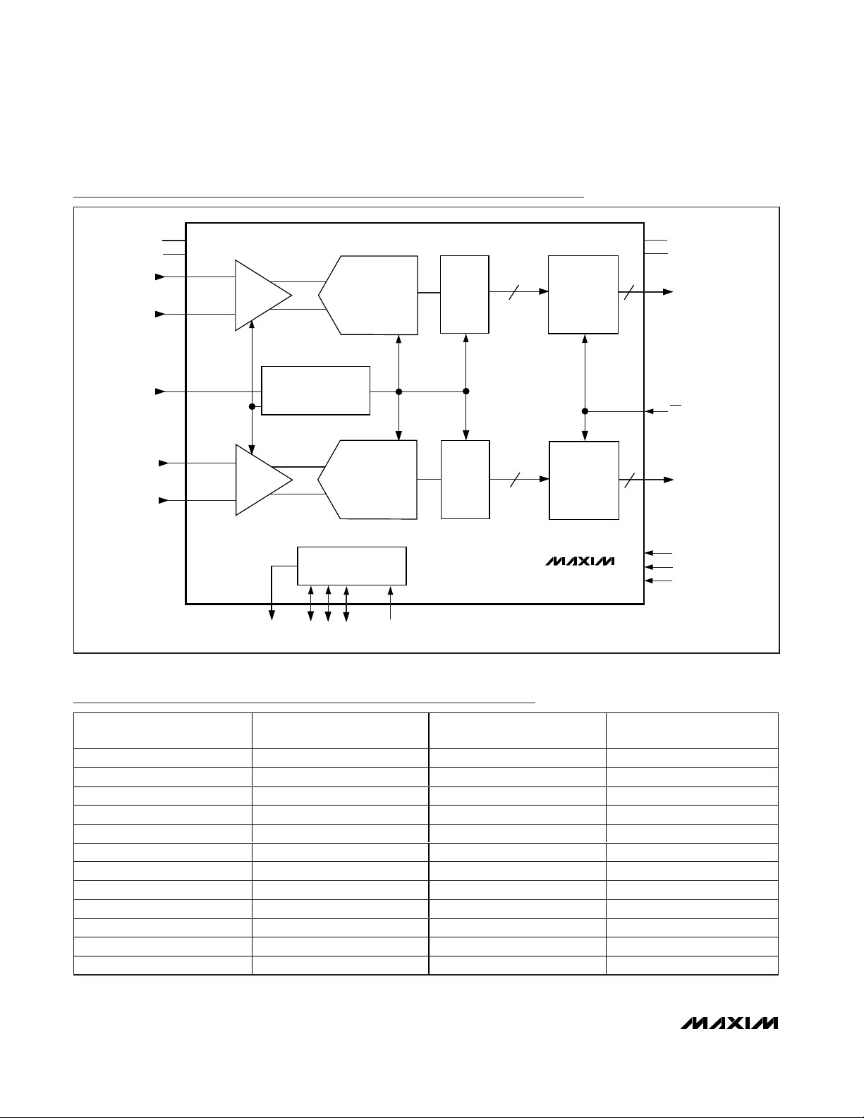
GND
REFERENCE
OUTPUT
DRIVERS
CONTROL
T/H
T/H
PIPELINE
ADC
DEC
OUTPUT
DRIVERS
REFOUT
REFN
COM
REFP
REFIN
INA+
INA-
CLK
INB+
INB-
V
DD
DEC
PIPELINE
ADC
OGND
OV
DD
D9A–D0A
OE
D9B–D0B
T/B
PD
SLEEP
MAX1182
10
10
10
10
Functional Diagram
20 ______________________________________________________________________________________
PART
RESOLUTION
(Bits)
SPEED GRADE
(Msps)
OUTPUT BUS
MAX1190 10 120 Full duplex
MAX1180 10 105 Full duplex
MAX1181 10 80 Full duplex
MAX1182 10 65 Full duplex
MAX1183 10 40 Full duplex
MAX1186 10 40 Half duplex
MAX1184 10 20 Full duplex
MAX1185 10 20 Half duplex
MAX1198 8 100 Full duplex
MAX1197 8 60 Full duplex
MAX1196 8 40 Half duplex
MAX1195 8 40 Full duplex
Pin-Compatible Versions
MAX1182
Dual 10-Bit, 65Msps, 3V, Low-Power ADC
with Internal Reference and Parallel Outputs
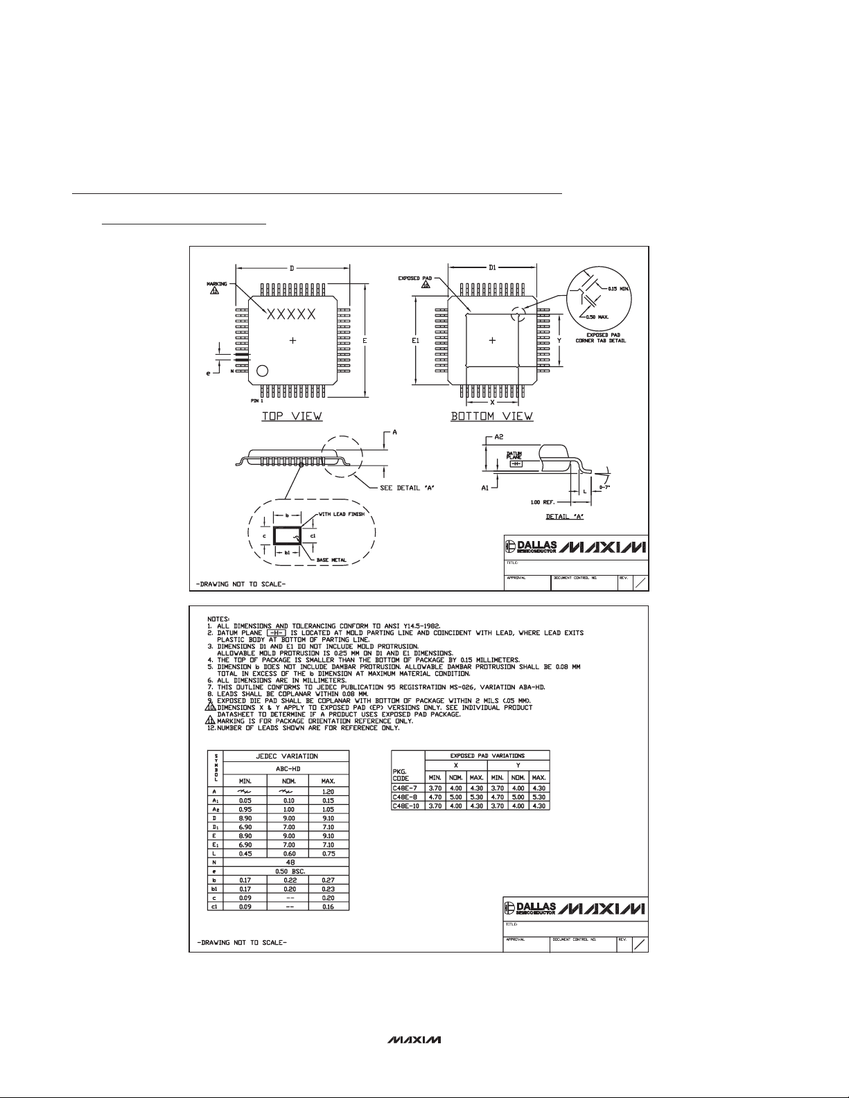
48L,TQFP.EPS
G
1
2
21-0065
PACKAGE OUTLINE,
48L TQFP, 7x7x1.0mm EP OPTION
G
2
2
21-0065
PACKAGE OUTLINE,
48L TQFP, 7x7x1.0mm EP OPTION
Maxim cannot assume responsibility for use of any circuitry other than circuitry entirely embodied in a Maxim product. No circuit patent licenses are
implied. Maxim reserves the right to change the circuitry and specifications without notice at any time.
Maxim Integrated Products, 120 San Gabriel Drive, Sunnyvale, CA 94086 408-737-7600 ____________________ 21
© 2006 Maxim Integrated Products Printed USA is a registered trademark of Maxim Integrated Products, Inc.
Package Information
(The package drawing(s) in this data sheet may not reflect the most current specifications. For the latest package outline information
go to www.maxim-ic.com/packages
.)
 Loading...