

19-1190; Rev 0; 3/97
_______________General Description
The MAX1161 10-bit, monolithic analog-to-digital converter (ADC) is capable of 40Msps minimum word
rates. An on-board track/hold ensures excellent dynamic performance without the need for external components. A 5pF input capacitance minimizes drive
requirement problems.
Inputs and outputs are TTL compatible. An overrange
output is provided to indicate overflow conditions.
Output data format is straight binary. Power dissipation
is low at only 1W with +5V and -5.2V power-supply voltages. The MAX1161 also accepts wide, ±2V input voltages.
The MAX1161 is available in 28-pin DIP and SO packages in the commercial temperature range.
________________________Applications
Medical Imaging
Professional Video
Radar Receivers
Instrumentation
Digital Communications
____________________________Features
♦ Monolithic 40Msps Converter
♦ On-Chip Track/Hold
♦ Bipolar, ±2V Analog Input
♦ 57dB SNR at 3.58MHz Input
♦ 5pF Input Capacitance
♦ TTL Outputs
MAX1161
10-Bit, 40Msps, TTL-Output ADC
________________________________________________________________
Maxim Integrated Products
1
For the latest literature: http://www.maxim-ic.com, or phone 1-800-998-8800
PART
MAX1161ACPI
MAX1161BCPI
MAX1161ACWI 0°C to +70°C
0°C to +70°C
0°C to +70°C
TEMP. RANGE PIN-PACKAGE
28 Wide Plastic DIP
28 Wide Plastic DIP
28 SO
MAX1161BCWI 0°C to +70°C 28 SO
______________Ordering Information
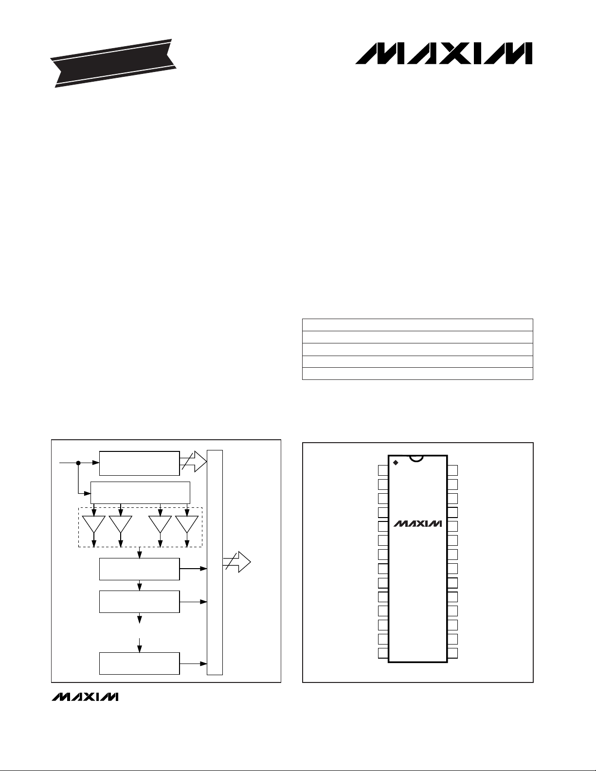
________________Functional Diagram
COARSE
ADC
T/H
AMPLIFIER
BANK
SUCCESSIVE INTERPOLATION
STAGE i
SUCCESSIVE INTERPOLATION
STAGE i + 1
SUCCESSIVE INTERPOLATION
STAGE N
ANALOG
PRESCALER
ANALOG
INPUT
4
10
DIGITAL
OUTPUT
DECODING NETWORK
.
.
.
.
__________________Pin Configuration
28
27
26
25
24
23
22
21
20
19
18
17
16
15
1
2
3
4
5
6
7
8
9
10
11
12
13
14
DIP/SO
DV
CC
V
EE
AGND
V
CC
VFB
VSB
VRM
VIN
VST
VFT
V
CC
AGND
V
EE
CLK
DGND
D0
D1
D2
D3
D4
D5
D6
D7
D8
D9
D10
DGND
DV
CC
MAX1161
TOP VIEW
EVALUATION KIT
AVAILABLE
TOP VIEW
MAX1161
10-Bit, 40Msps, TTL-Output ADC
2 _______________________________________________________________________________________
ABSOLUTE MAXIMUM RATINGS
ELECTRICAL CHARACTERISTICS
(VCC= +5.0V, VEE= -5.2V, DVCC= +5.0V, VIN= ±2.0V, VSB = -2.0V, VST = +2.0V, f
CLK
= 40MHz, 50% clock duty cycle,
T
A
= T
MIN
to T
MAX
, unless otherwise noted.)
Stresses beyond those listed under “Absolute Maximum Ratings” may cause permanent damage to the device. These are stress ratings only, and functional
operation of the device at these or any other conditions beyond those indicated in the operational sections of the specifications is not implied. Exposure to
absolute maximum rating conditions for extended periods may affect device reliability.
VCC........................................................................................+6V
V
EE
..........................................................................................-6V
Analog Input.......................................................VFB ≤ VIN ≤ VFT
VFT
,
VFB ...........................................................................3V, -3V
Reference-Ladder Current..................................................12mA
CLK Input...............................................................................V
CC
Digital Outputs.....................................................30mA to -30mA
Continuous Power Dissipation (T
A
= +70°C)
Plastic DIP........................................................................1.14W
SO .........................................................................................1W
Operating Temperature Range...............................0°C to +70°C
Junction Temperature......................................................+150°C
Storage Temperature Range.............................-65°C to +150°C
Lead Temperature (soldering, 10sec).............................+300°C
V
V
V
I
VI
V
I
VI
V
VI
VI
VI
V
VI
VI
V
VI
LSB
VI
TEST
LEVEL
ns12TA= +25°CAcquisition Time
ps-RMS5TA= +25°CAperture Jitter Time
ns14 18TA= +25°C
Output Delay
Clock
Cycle
1Pipeline Delay (Latency)
ns20Overvoltage Recovery Time
MHz40Maximum Conversion Rate
Ω/°C0.8
Reference-Ladder
Tempco
Ω500 800
Reference-Ladder
Resistance
MHz1203dB small signalInput Bandwidth
pF5Input Capacitance
kΩ75 300TA= -55°C to +125°CInput Resistance
LSB±0.5Differential Nonlinearity
LSB±1.0
Bits10Resolution
Integral Nonlinearity
kΩ100 300Input Resistance
µA75TA= -55°C to +125°CInput Bias Current
µA30 60VIN= 0VInput Bias Current
V±2.0Input Voltage Range
GuaranteedNo Missing Codes
±2.0Positive Full-Scale Error ±2.0
V LSB±2.0
UNITS
MAX1161A
MIN TYP MAX
CONDITIONSPARAMETER
12
5
14 18
1
20
40
0.8
500 800
120
5
75 300
±0.75
±1.5
10
100 300
75
30 60
±2.0
Guaranteed
Negative Full-Scale Error ±2.0
MAX1161B
MIN TYP MAX
V ns1TA= +25°C
Aperture Delay Time
1
DC ACCURACY (±full scale, 250kHz sample rate, TA= +25°C)
ANALOG INPUT
REFERENCE INPUT
TIMING CHARACTERISTICS
MAX1161
10-Bit, 40Msps, TTL-Output ADC
_______________________________________________________________________________________
3
ELECTRICAL CHARACTERISTICS (continued)
(VCC= +5.0V, VEE= -5.2V, DVCC= +5.0V, VIN= ±2.0V, VSB = -2.0V, VST = +2.0V, f
CLK
= 40MHz, 50% clock duty cycle,
T
A
= T
MIN
to T
MAX
, unless otherwise noted.)
TA= +25°C
TA= 0°C to +70°C,
T
A
= -25°C to +85°C
fIN= 1MHz
52 54
50 52
TA= +25°C
53 55
TA= 0°C to +70°C,
TA= -25°C to +85°C
IV
55 57I
fIN= 10.0MHz
fIN= 3.58MHz
fIN= 1MHz
MAX1161B
MIN TYP MAX
8.2
8.2
6.9
Effective Number of Bits
(ENOB)
7.3
Bits
PARAMETER CONDITIONS
MAX1161A
MIN TYP MAX
UNITS
8.7
8.7
TEST
LEVEL
TA= +25°C
TA= 0°C to +70°C,
TA= -25°C to +85°C
fIN= 3.58MHz
52 54
50 52
fIN= 1MHz
53 55
52 54
IV
55 57I
TA= +25°C
TA= 0°C to +70°C,
TA= -25°C to +85°C
fIN= 10.0MHz
46 48
43 45
Signal-to-Noise Ratio
(without harmonics)
(SNR)
45 47
dB
IV
48 50I
49 5151 53IV
54 56I
TA= +25°C
TA= 0°C to +70°C,
TA= -25°C to +85°C
fIN= 3.58MHz
52 54
49 5151 53IV
54 56I
TA= +25°C
TA= 0°C to +70°C,
TA= -25°C to +85°C
fIN= 10.0MHz
43 45
41 44
Total Harmonic Distortion
(THD)
45 47
dB
IV
46 48I
TA= +25°C
TA= 0°C to +70°C,
TA= -25°C to +85°C
fIN= 1MHz
49 51
4649IV
52 54I
TA= +25°C
TA= 0°C to +70°C,
TA= -25°C to +85°C
fIN= 3.58MHz
49 51
4649IV
52 54I
TA= +25°C
TA= 0°C to +70°C,
TA= -25°C to +85°C
fIN= 10.0MHz
41 43
40
Signal-to-Noise and
Distortion Ratio
(SINAD)
43
dB
IV
44 46I
TA= +25°C 6767V
fIN= 3.58MHz,
4.35MHz
fIN= 1MHz
0.2V 0.2 Degrees
dB
Differential Phase
Spurious-Free
Dynamic Range (SFDR)
TA= +25°C
fIN= 3.58MHz,
4.35MHz
0.5V 0.7 %Differential Gain
DYNAMIC PERFORMANCE
TA= +25°C

MAX1161
10-Bit, 40Msps, TTL-Output ADC
4 _______________________________________________________________________________________
V V2.4 4.5Logic 1 Voltage 2.4 4.0
IV µA0 5 20TA= +25°C
Maximum Input
Current Low
0 5 20
V V0.8Logic 0 Voltage 0.8
Pulse Width High (CLK) ns10 300IV 10 300
Maximum Input
Current High
Pulse Width Low (CLK)
µA
ns10IV 10
IV 0 5 20 0 5 20TA= +25°C
TEST
LEVEL
UNITS
MAX1161A
MIN TYP MAX
CONDITIONSPARAMETER
MAX1161B
MIN TYP MAX
Logic 1 Voltage V2.4IV 2.4
Logic 0 Voltage V0.6IV 0.6
LSB
4.75 5.0 5.25IV 4.75 5.0 5.25DV
CC
W
4.75 5.25IV 4.75 5.25V
CC
Power Dissipation 1.0 1.3VI 1.0 1.3
Voltages
-4.95 -5.2 -5.45IV -4.95 -5.2 -5.45-V
EE
Power-Supply Rejection
V
1.0V 1.0VCC= 5V ±0.25V, VEE= -5.2V ±0.25V
ELECTRICAL CHARACTERISTICS (continued)
(VCC= +5.0V, VEE= -5.2V, DVCC= +5.0V, VIN= ±2.0V, VSB = -2.0V, VST = +2.0V, f
CLK
= 40MHz, 50% clock duty cycle,
T
A
= T
MIN
to T
MAX
, unless otherwise noted.)
TEST LEVEL CODES
All electrical characteristics are subject to the following conditions:
All parameters having min/max specifications are guaranteed. The
Test Level column indicates the specific device testing actually performed during production and Quality Assurance inspection. Any
blank section in the data column indicates that the specification is
not tested at the specified condition.
Unless otherwise noted, all tests are pulsed; therefore, Tj= TC= TA.
TEST LEVEL
I
II
III
IV
V
VI
TEST PROCEDURE
100% production tested at the specified temperature.
100% production tested at TA = +25°C, and sample tested at the specified
temperatures.
QA sample tested only at the specified temperatures.
Parameter is guaranteed (but not tested) by design and characterization data.
Parameter is a typical value for information purposes only.
100% production tested at TA = +25°C. Parameter is guaranteed over specified
temperature range.
40 55VI 40 55DI
CC
118 145VI 118 145I
CC
Currents
40 57VI 40 57-I
EE
mA
DIGITAL INPUTS
DIGITAL OUTPUTS
POWER-SUPPLY REQUIREMENTS
______________________________________________________________Pin Description
NAME
1, 13 DGND
2 D0
PIN
12 D10
15 CLK
3–10
FUNCTION
16, 27 V
EE
Digital Ground
D1–D8
TTL Output (LSB)
TTL Outputs
11 D9 TTL Output (MSB)
14, 28 DV
CC
+5V Supply (digital)
TTL Output Overrange
Clock
-5.2V Supply (analog)
NAME
20 VST
19
PIN
VFT
21
18, 25 V
CC
VIN
FUNCTION
22
17, 26 AGND
VRM
23 VSB
Sense for Top of Reference Ladder
24 VFB
Force for Top of Reference Ladder
+5V Supply (analog)
Analog Input
Analog Ground
Middle of Voltage Reference Ladder
Sense for Bottom of Reference Ladder
Force for Bottom of Reference Ladder

MAX1161
10-Bit, 40Msps, TTL-Output ADC
_______________________________________________________________________________________ 5
__________________________________________Typical Operating Characteristics
(TA= +25°C, unless otherwise noted.)
80
20
1 10 100
TOTAL HARMONIC DISTORTION vs.
INPUT FREQUENCY
40
30
MAX1161-01
INPUT FREQUENCY (MHz)
THD (dB)
60
50
70
fS = 40Msps
80
20
1 10 100
SIGNAL-TO-NOISE AND DISTORTION
vs. INPUT FREQUENCY
40
30
MAX1161-03
INPUT FREQUENCY (MHz)
SINAD (dB)
60
50
70
fS = 40Msps
80
20
1 10 100
SNR, THD, SINAD vs.
SAMPLE RATE
40
30
MAX1161-04
SAMPLE RATE (Msps)
SNR, THD, SINAD (dB)
60
50
70
SINAD
SNR
fIN = 1MHz
THD
65
40
-25 50 750 25
SNR, THD, SINAD vs.
TEMPERATURE
50
45
MAX1161-06
TEMPERATURE (°C)
SNR, THD, SINAD (dB)
60
55
fS = 40Msps
f
IN
= 1MHz
THD
SNR
SINAD
0
-120
0 6 8 102 4
SPECTRAL RESPONSE
-60
-90
MAX1161-05
INPUT FREQUENCY (MHz)
AMPLITUDE (dB)
-30
fS = 40Msps
f
IN
= 1MHz
80
20
1 10 100
SIGNAL-TO-NOISE vs.
INPUT FREQUENCY
40
30
MAX1161-02
INPUT FREQUENCY (MHz)
SNR (dB)
60
50
70
fS = 40Msps
_______________Detailed Description
The MAX1161 requires few external components to
achieve the stated operation and performance. Figure 2
shows the typical interface requirements when using the
MAX1161 in normal circuit operation. The following section provides a description of the pin functions, and outlines critical performance criteria to consider for
achieving optimal device performance.
Power Supplies and Grounding
The MAX1161 requires -5.2V and +5V analog supply
voltages. The +5V supply is common to analog VCCand
digital DVCC. A ferrite bead in series with each supply
line reduces the transient noise injected into the analog
V
CC
. These beads should be connected as close to the
device as possible. The connection between the beads
and the MAX1161 should not be shared with any other
device. Bypass each power-supply pin as close to the
device as possible. Use 0.1µF for VEEand VCC, and
0.01µF for DVCC(chip capacitors are recommended).
The MAX1161 has two grounds: AGND and DGND.
These internal grounds are isolated on the device. Use
ground planes for optimum device performance.
Use DGND for the DVCCreturn path (typically 40mA)
and for the return path for all digital output logic interfaces. Separate AGND and DGND from each other,
connecting them together only through a ferrite bead at
the device.

Connect a Schottky or hot carrier diode between AGND
and VEE. The use of separate power supplies between
VCCand DV
CC
is not recommended due to potential
power-supply-sequencing latchup conditions. For optimum performance, use the recommended circuit
shown in Figure 2.
Voltage Reference
The MAX1161 requires the use of two voltage references: VFT and VFB. VFT is the force for the top of the
voltage-reference ladder (typically +2.5V); VFB (typically -2.5V) is the force for the bottom of the voltagereference ladder. Both voltages are applied across an
800Ω internal reference-ladder resistance. The +2.5V
voltage source for reference VFT must be current limited
to 20mA (max) if a different driving circuit is used in
place of the recommended reference circuit shown in
Figures 2 and 3. In addition, there are three referenceladder taps (VST, VRM, and VSB). VST is the sense for
the top of the reference ladder (+2V), VRM is the midpoint of the ladder (typically 0V), and VSB is the sense
for the bottom of the reference ladder (-2V). The voltages at VST and VSB are the device’s true full-scale
input voltages when VFT and VFB are driven to the recommended voltages (+2.5V and -2.5V, respectively).
These points should be used to monitor the device’s
actual full-scale input range. When not being used, a
decoupling capacitor of 0.01µF (chip carrier preferred)
connected to AGND from each tap is recommended to
minimize high-frequency noise injection.
Figure 2 shows an example of a recommended reference-driver circuit. IC1 (MAX6225) is a +2.5V reference
with 0.2% accuracy. Potentiometer R1 is 10kΩ and supports a minimum adjustable range of 0.6%. Use an
OP07 or equivalent device for IC2. R2 and R3 must be
matched to within 0.1% with good TC tracking to maintain 0.3LSB matching between VFT and VFB. If 0.1%
matching is not met, then R4 can be used to adjust the
VFB voltage to the desired level. Adjust VFT and VFB
such that VST and VSB are exactly +2V and -2V,
respectively.
The analog input range scales proportionally with respect
to the reference voltage if a different input range is
required. The maximum scaling factor for device operation is ±20% of the recommended reference voltages of
VFT and VFB. However, because the device is laser
trimmed to optimize performance with ±2.5V references,
its accuracy degrades if operated beyond a ±2% range.
The following errors are defined:
+FS error = top of ladder offset voltage
= ∆ (+FS - VST + 1LSB)
-FS error = bottom of ladder offset voltage
= ∆ (-FS - VSB - 1LSB)
where the +FS (full-scale) input voltage is defined as the
output transition between 11 1111 1110 and 11 1111 1111,
and the -FS input voltage is defined as the output transition between 00 0000 0000 and 00 0000 0001 (Table 2).
MAX1161
10-Bit, 40Msps, TTL-Output ADC
6 _______________________________________________________________________________________
CLK
DATA VALID
t
d
OUTPUT
DATA
Figure 1b. Single-Event Clock
CLK
t
pwH
N - 2
N - 1
N
DATA VALID
N
DATA VALID
N + 1
t
pwL
t
d
N + 1
N + 2
OUTPUT
DATA
Figure 1a. Timing Diagram
DESCRIPTION UNITS
t
d
CLK to Data Valid Propagation Delay ns
t
pwH
CLK High Pulse Width ns
PARAMETER
10 300
t
pwL
CLK Low Pulse Width ns10
MIN TYP MAX
14 18
Table 1. Timing Parameters

Analog Input
VIN is the analog input. The full-scale input range will be
80% of the reference voltage, or ±2V with VFB =
-2.5V and VFT = +2.5V.
The analog input’s drive requirements are minimal
when compared to conventional flash converters. This
is due to the MAX1161’s extremely low (5pF) input
capacitance and very high (300kΩ) input resistance.
For example, for an input signal of ±2Vp-p with a
10MHz input frequency, the peak output current
required for the driving circuit is only 628µA.
MAX1161
10-Bit, 40Msps, TTL-Output ADC
_______________________________________________________________________________________ 7
COARSE
ADC
SUCCESSIVE
INTERPOLATION
STAGE 1
SUCCESSIVE
INTERPOLATION
STAGE N
DIGITAL
OUTPUTS
DECODING NETWORK
VEEVEEAGND
AGND
VCCVCCDVCCDVCCDGND
DGND
FB
FB
FB
+5V
-5.2V
-2.5V
+5V
IC1
IC2
OP07
R1
10k
R2
30k
R3
30k
R4
10k
1µF
0.01µF
0.01µF
1µF
10µF
10µF
1µF
C1
0.01µF
C2
0.01µF
C3
0.01µF
C4
0.01µF
C6
0.1µF
C7
0.1µF
C8
0.1µF
C9
0.1µF
C10
0.01µF
C11
0.01µF
C5
0.01µF
VIN
(±2V)
±2.5V MAX
CLK
(TTL)
VIN
VFT
VIN
CLK
4
VST
VRM
VSB
VFB
GND
VOUT
VTRIM
R5
100Ω
2.5V
1
3
2
4
6
7
8
R
2R
2R
2R
2R
R
D1
-5.2V
= AGND
+5V
DGNDAGND
= DGND
D10
D9
D8
D7
D6
D5
D4
D3
D2
D1
D0
2
4
5
6
NOTES:
1) D1 = SCHOTTKY OR HOT CARRIER DIODE
2) FB = FERRITE BEAD, FAIR RITE #2743001111
TO BE MOUNTED AS CLOSELY TO THE DEVICE
AS POSSIBLE. THE FERRITE BEAD TO ADC
CONNECTION SHOULD NOT BE SHARED WITH
ANY OTHER DEVICE.
3) C1–C11 = CHIP CAPACITOR (RECOMMENDED)
MOUNTED AS CLOSE TO DEVICE'S PIN AS
POSSIBLE.
4) USE OF A SEPARATE SUPPLY FOR V
CC
AND DVCC
IS NOT RECOMMENDED.
5) R5 PROVIDES CURRENT LIMITING TO 45mA.
(OVERRANGE)
(MSB)
(LSB)
ANALOG
PRESCALER
MAX1161
MAX6225
Figure 2. Typical Operating Circuit
Figure 3. Analog Equivalent Input Circuit
VIN VFT
V
CC
V
EE
ANALOG PRESCALER

Maxim cannot assume responsibility for use of any circuitry other than circuitry entirely embodied in a Maxim product. No circuit patent licenses are
implied. Maxim reserves the right to change the circuitry and specifications without notice at any time.
8
___________________Maxim Integrated Products, 120 San Gabriel Drive, Sunnyvale, CA 94086 (408) 737-7600
© 1997 Maxim Integrated Products Printed USA is a registered trademark of Maxim Integrated Products.
MAX1161
10-Bit, 40Msps, TTL-Output ADC
Clock Input
The MAX1161 is driven from a single-ended TTL input
(CLK). The CLK pulse width (t
pwH
) must be kept
between 10ns and 300ns to ensure proper operation of
the internal track/hold amplifier (Figure 1a). When operating the MAX1161 at sampling rates above 3Msps, it is
recommended that the clock input duty cycle be kept
at 50% to optimize performance (Figure 4). The analog
input signal is latched on the rising edge of CLK.
The clock input must be driven from fast TTL logic (VIH
≤ 4.5V, t
RISE
<6ns). In the event the clock is driven from
a high current source, use a 100Ω resistor (R5) in
series to limit current to approximately 45mA.
Digital Outputs
The format of the output data (D0–D9) is straight binary
(Table 2). The outputs are latched on the rising edge of
CLK with a propagation delay typically at 14ns. There is
a one-clock-cycle latency between CLK and the valid
output data (Figure 1a).
The digital outputs’ rise and fall times are not symmetrical. Typical propagation delay is 14ns for the rise time
and 6ns for the fall time (Figure 5). The nonsymmetrical
rise and fall times create approximately 8ns of invalid
data.
Overrange Output
The overrange output (D10) is an indication that the
analog input signal has exceeded the positive full-scale
input voltage by 1LSB. When this condition occurs, D10
will switch to logic 1. All other data outputs (D0–D9) will
remain at logic 1 as long as D10 remains at logic 1.
This feature makes it possible to include the MAX1161
in higher-resolution systems.
Evaluation Board
The MAX1160 EV kit is available to help designers
demonstrate the MAX1160 or MAX1161’s full performance. This board includes a reference circuit, clockdriver circuit, output data latches, and an on-board
reconstruction of the digital data. A separate data sheet
describing the operation of this board is also available.
Contact the factory for price and availability.
43
25 60 65 70 7535 4030 45 50 55
51
53
45
47
49
DUTY CYCLE OF POSITIVE CLOCK PULSE (°C)
SIGNAL-TO-NOISE-RATIO (dB)
57
59
55
t
pwH
t
pwL
DUTY CYCLE =
t
pwH
t
pwL
ANALOG
INPUT
> +2V + 1/2LSB
+2V - 1LSB
0.0V 0
0
1
OVERRANGE
D10
OUTPUT CODE
D9–D0
11 1111 1111
11 1111 111
Ø
ØØ ØØØØ ØØØØ
-2V + 1LSB 0 00 0000 000
Ø
< 2V 0 00 0000 0000
Table 2. Output Data Information
CLK IN
DATA
OUT
(ACTUAL)
2.4V
3.5V
2.4V
0.5V
0.8V
t
pd1
typ
6ns
N
N + 1
DATA OUT
(EQUIVALENT)
(N - 1) N
(N - 1)
N
t
RISE
6ns
(N - 2)
(N - 2)
14ns typ
INVALID
DATA
INVALID
DATA
INVALID
DATA
INVALID
DATA
Figure 5. Digital Output Characteristics
(Øindicates the flickering bit between logic 0 and 1.)
Figure 4. SNR vs. Clock Duty Cycle
 Loading...