19-1170; Rev 0; 12/96
EVALUATION KIT
AVAILABLE
8-Bit, 750Msps Flash ADC
_______________General Description
The MAX1151 is a parallel flash analog-to-digital converter (ADC) capable of digitizing full-scale (0V to -2V)
inputs into 8-bit digital words at an update rate of
750Msps. The ECL-compatible outputs are demuxed
into two separate output banks, each with differential
data-ready outputs to ease the task of data capture.
The MAX1151’s wide input bandwidth and low capaci-
____________________________Features
♦ 1:2 Demuxed ECL-Compatible Outputs
♦ Wide Input Bandwidth: 900MHz
♦ Low Input Capacitance: 15pF
♦ Metastable Errors Reduced to 1LSB
♦ Single -5.2V Supply
tance eliminate the need for external track/hold amplifiers for most applications. A proprietary decoding
scheme reduces metastable errors to 1LSB. This device
operates from a single -5.2V supply, with a nominal
power dissipation of 5.5W.
________________________Applications
Digital Oscilloscopes
Data Acquisition
Transient-Capture Applications
______________Ordering Information
PART
MAX1151AIZS
MAX1151BIZS -20°C to +85°C
TEMP. RANGE PIN-PACKAGE
-20°C to +85°C
80 MQUAD
80 MQUAD
Radar, EW, ECM
Direct RF/IF Downconversion
Pin Configuration appears on last page.
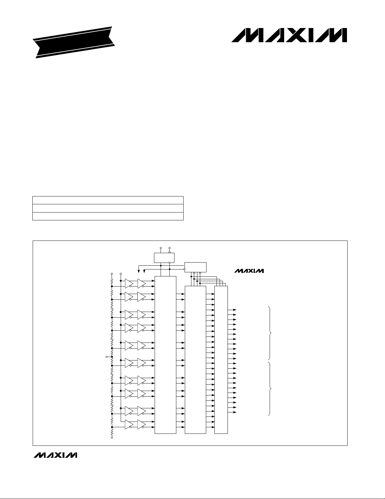
_________________________________________________________Functional Diagram
CLK NCLK
CLOCK
BUFFER
ANALOG
VRT
INPUT
COMPARATOR
PREAMP
255
DEMUX
CLOCK BUFFER
MAX1151
MAX1151
VRM
254
152
151
128
127
64
63
2
1
VFB
D8
(OVR)
D7
(MSB)
D6
D5
D4
256-BIT TO 8-BIT DECODER
WITH METASTABLE ERROR CORRECTION
D3
D2
D1
D0
(LSB)
________________________________________________________________
1:2 DEMULTIPLEXER
D8B
D7B
•
•
D5B
•
•
D2B
D1B
D0B
D8A
D7A
•
•
•
D5A
•
•
•
D2A
D1A
D0A
ECL OUTPUT BUFFERS AND LATCHES
NDRB (NOT DATA READY)
DRB (DATA READY)
D8B (OVR)
D7B (MSB)
D6B
D5B
D4B
D3B
D2B
D1B
D0B (LSB)
NDRA (NOT DATA READY)
DRA (DATA READY)
D8A (OVR)
D7A (MSB)
D6A
D5A
D4A
D3A
D2A
D1A
D0A (LSB)
BANK B
BANK A
Maxim Integrated Products
For the latest literature: http://www.maxim-ic.com, or phone 1-800-998-8800
1

8-Bit, 750Msps Flash ADC
ABSOLUTE MAXIMUM RATINGS
Supply Voltages
Negative Supply Voltage (V
Ground Voltage Differential.................................-0.5V to +0.5V
Input Voltages
Analog Input Voltage.............................................+0.5V to V
Reference Input Voltage........................................+0.5V to V
Digital Input Voltage ..............................................+0.5V to V
Reference Current (VRTto VRB)........................................35mA
MAX1151
Stresses beyond those listed under “Absolute Maximum Ratings” may cause permanent damage to the device. These are stress ratings only, and functional
operation of the device at these or any other conditions beyond those indicated in the operational sections of the specifications is not implied. Exposure to
absolute maximum rating conditions for extended periods may affect device reliability.
to GND) .............-7.0V to +0.5V
EE
EE
EE
EE
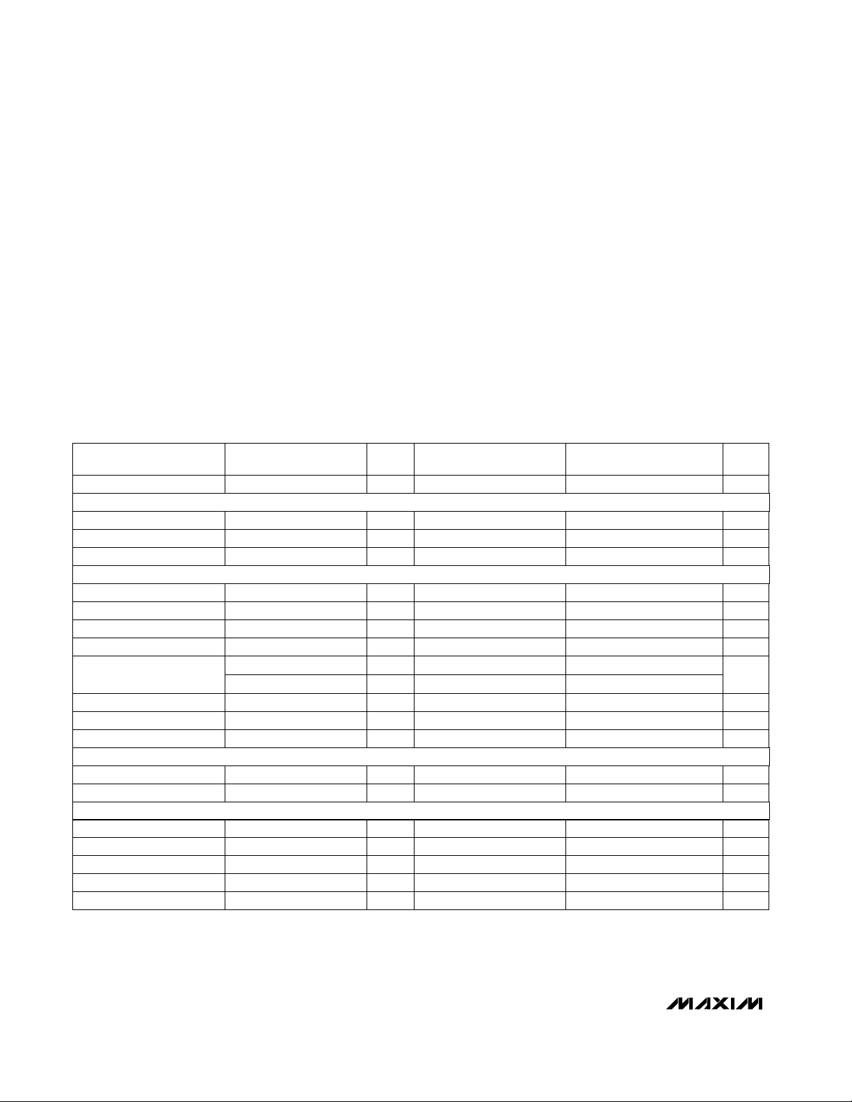
ELECTRICAL CHARACTERISTICS
(VEE= -5.2V, V
= TC= TA= +25°C.) (Note 1)
T
j
DC ACCURACY
Integral Nonlinearity
ANALOG INPUT
Input Voltage Range
Input Capacitance
Input Bandwidth
REFERENCE INPUT
TIMING CHARACTERISTICS
CLK to DATA READY Delay
= -2.00V, VRM= -1.00V, VRT= 0.00V, f
RB
CONDITIONSPARAMETER
= 100kHz
CLK
= 100kHzDifferential Nonlinearity
CLK
Small signal
Large signal V 500 500
RT
RB
= 750MHz, duty cycle = 50%, typical thermal impedance (θJC) = 4°C/W,
CLK
TEST
LEVEL
I
I
I
I
V
V
V
IV
IV mV-30 30Offset Error V
V V/ns5Input Slew Rate 5
I
V
I
V
V
IV
IV
Digital Output Current ...........................................0mA to -28mA
Operating Temperature Range ...........................-20°C to +85°C
Case Temperature...........................................................+125°C
Junction Temperature......................................................+150°C
Lead Temperature (soldering, 10sec).............................+300°C
Storage Temperature Range.............................-65°C to +150°C
MAX1151A
MIN TYP MAX
GuaranteedNo Missing Codes
RB
900
V
RT
MAX1151B
MIN TYP MAX
8
-1.5 1.5
-0.95 1.5
Guaranteed
V
RB
0.75 2.0
15
15
900
-30 30
-30 30
60 80
30
750
2
250
0.9 1.4 1.9
1.25 1.75 2.25
V
UNITS
RT
Bits8Resolution
LSB-1.0 1.0f
LSB-0.85 0.95f
VV
mA0.75 2.0VIN= 0VInput Bias Current
kΩ15Input Resistance
pF15Over full input range
MHz
mV-30 30Offset Error V
Ω60 80Ladder Resistance
MHz30Reference Bandwidth
MHz750Maximum Sample Rate
ps2Aperture Jitter
ps250Acquisition Time
ns0.9 1.4 1.9
ns1.25 1.75 2.25Clock to Data Delay
2 _______________________________________________________________________________________

8-Bit, 750Msps Flash ADC
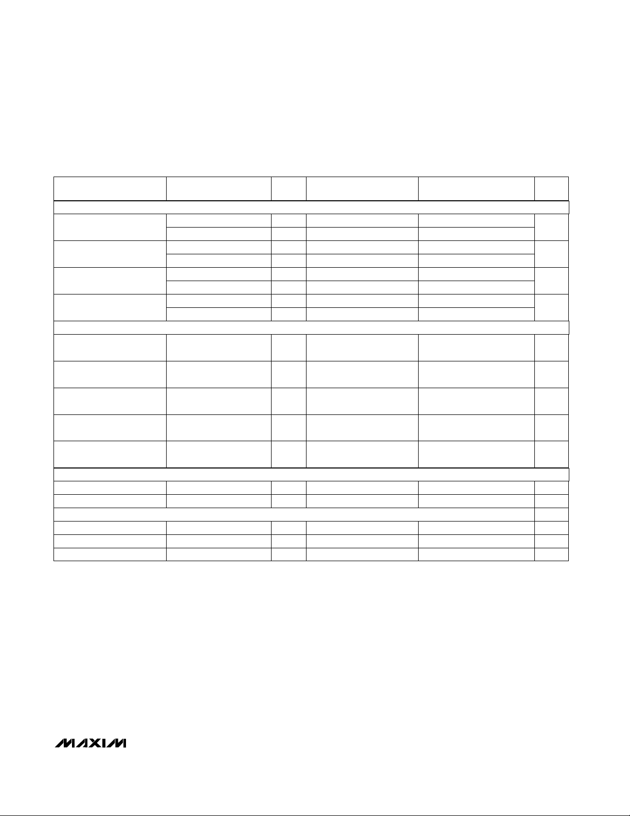
ELECTRICAL CHARACTERISTICS (continued)
(VEE= -5.2V, V
= TC= TA= +25°C.) (Note 1)
T
j
DYNAMIC PERFORMANCE
Signal-to-Noise Ratio
(without harmonics)
Total Harmonic Distortion
Signal-to-Noise and
Distortion
Spurious-Free Dynamic
Range
DIGITAL INPUTS
Input High Voltage
(CLK, NCLK)
Input Low Voltage
(CLK, NCLK)
Clock Pulse Width High
(t
)
PWH
Clock Pulse Width Low
(t
)
PWL
Clock Synchronous
Input Currents
DIGITAL OUTPUTS
POWER-SUPPLY REQUIREMENTS
= -2.00V, VRM= -1.00V, VRT= 0.00V, f
RB
CONDITIONSPARAMETER
fIN= 250MHz
= 750MHz, duty cycle = 50%, typical thermal impedance (θJC) = 4°C/W,
CLK
TEST
LEVEL
I
I
I
I
I
I
I
I
I
I
I 0.67 0.5 0.67 0.5 ns
V µA2
I
I
V
IV
I
I W5.5 6.25Power Dissipation 5.5 6.25
MAX1151A
MIN TYP MAX
46fIN= 50MHz
44
-45fIN= 50MHz
-37fIN= 250MHz
43fIN= 50MHz
48fIN= 50MHz
40fIN= 250MHz
2.4
MAX1151B
MIN TYP MAX
44
42
-43
-35
41
3436IfIN= 250MHz
44
36
-1.1 -0.7
-1.8 -1.5
0.67 0.5
2
-1.1 -0.9
-1.8 -1.5
2.4
-4.95 -5.2 -5.45
1.05 1.2
MAX1151
UNITS
dB
dBc
dB
dB
V-1.1 -0.7
V-1.8 -1.5
ns0.67 0.5
V-1.1 -0.9Logic "1" Voltage
V-1.8 -1.5Logic "0" Voltage
V-4.95 -5.2 -5.45Supply Voltage (VEE)
A1.05 1.2Supply Current (IEE)
Note 1: All parameters having min/max specifications are guaranteed. The Test Level column indicates the specific device testing actually
performed during production and Quality Assurance inspection. Unless otherwise noted, all tests are pulsed tests; therefore,
= TC = TA.
T
j
TEST LEVEL
I
II
III
IV
V
VI
TEST PROCEDURE
100% production tested at the specified temperature.
100% production tested at T
QA sample tested only at the specified temperatures.
Parameter is guaranteed (but not tested) by design and characterization data.
Parameter is a typical value for information purposes only.
100% production tested at T
_______________________________________________________________________________________ 3
= +25°C, and sample tested at the specified temperatures.
A
= +25°C. Parameter is guaranteed over specified temperature range.
A
 Loading...