

19-1170; Rev 0; 12/96
EVALUATION KIT
AVAILABLE
8-Bit, 750Msps Flash ADC
_______________General Description
The MAX1151 is a parallel flash analog-to-digital converter (ADC) capable of digitizing full-scale (0V to -2V)
inputs into 8-bit digital words at an update rate of
750Msps. The ECL-compatible outputs are demuxed
into two separate output banks, each with differential
data-ready outputs to ease the task of data capture.
The MAX1151’s wide input bandwidth and low capaci-
____________________________Features
♦ 1:2 Demuxed ECL-Compatible Outputs
♦ Wide Input Bandwidth: 900MHz
♦ Low Input Capacitance: 15pF
♦ Metastable Errors Reduced to 1LSB
♦ Single -5.2V Supply
tance eliminate the need for external track/hold amplifiers for most applications. A proprietary decoding
scheme reduces metastable errors to 1LSB. This device
operates from a single -5.2V supply, with a nominal
power dissipation of 5.5W.
________________________Applications
Digital Oscilloscopes
Data Acquisition
Transient-Capture Applications
______________Ordering Information
PART
MAX1151AIZS
MAX1151BIZS -20°C to +85°C
TEMP. RANGE PIN-PACKAGE
-20°C to +85°C
80 MQUAD
80 MQUAD
Radar, EW, ECM
Direct RF/IF Downconversion
Pin Configuration appears on last page.
_________________________________________________________Functional Diagram
CLK NCLK
CLOCK
BUFFER
ANALOG
VRT
INPUT
COMPARATOR
PREAMP
255
DEMUX
CLOCK BUFFER
MAX1151
MAX1151
VRM
254
152
151
128
127
64
63
2
1
VFB
D8
(OVR)
D7
(MSB)
D6
D5
D4
256-BIT TO 8-BIT DECODER
WITH METASTABLE ERROR CORRECTION
D3
D2
D1
D0
(LSB)
________________________________________________________________
1:2 DEMULTIPLEXER
D8B
D7B
•
•
D5B
•
•
D2B
D1B
D0B
D8A
D7A
•
•
•
D5A
•
•
•
D2A
D1A
D0A
ECL OUTPUT BUFFERS AND LATCHES
NDRB (NOT DATA READY)
DRB (DATA READY)
D8B (OVR)
D7B (MSB)
D6B
D5B
D4B
D3B
D2B
D1B
D0B (LSB)
NDRA (NOT DATA READY)
DRA (DATA READY)
D8A (OVR)
D7A (MSB)
D6A
D5A
D4A
D3A
D2A
D1A
D0A (LSB)
BANK B
BANK A
Maxim Integrated Products
For the latest literature: http://www.maxim-ic.com, or phone 1-800-998-8800
1
8-Bit, 750Msps Flash ADC
ABSOLUTE MAXIMUM RATINGS
Supply Voltages
Negative Supply Voltage (V
Ground Voltage Differential.................................-0.5V to +0.5V
Input Voltages
Analog Input Voltage.............................................+0.5V to V
Reference Input Voltage........................................+0.5V to V
Digital Input Voltage ..............................................+0.5V to V
Reference Current (VRTto VRB)........................................35mA
MAX1151
Stresses beyond those listed under “Absolute Maximum Ratings” may cause permanent damage to the device. These are stress ratings only, and functional
operation of the device at these or any other conditions beyond those indicated in the operational sections of the specifications is not implied. Exposure to
absolute maximum rating conditions for extended periods may affect device reliability.
to GND) .............-7.0V to +0.5V
EE
EE
EE
EE
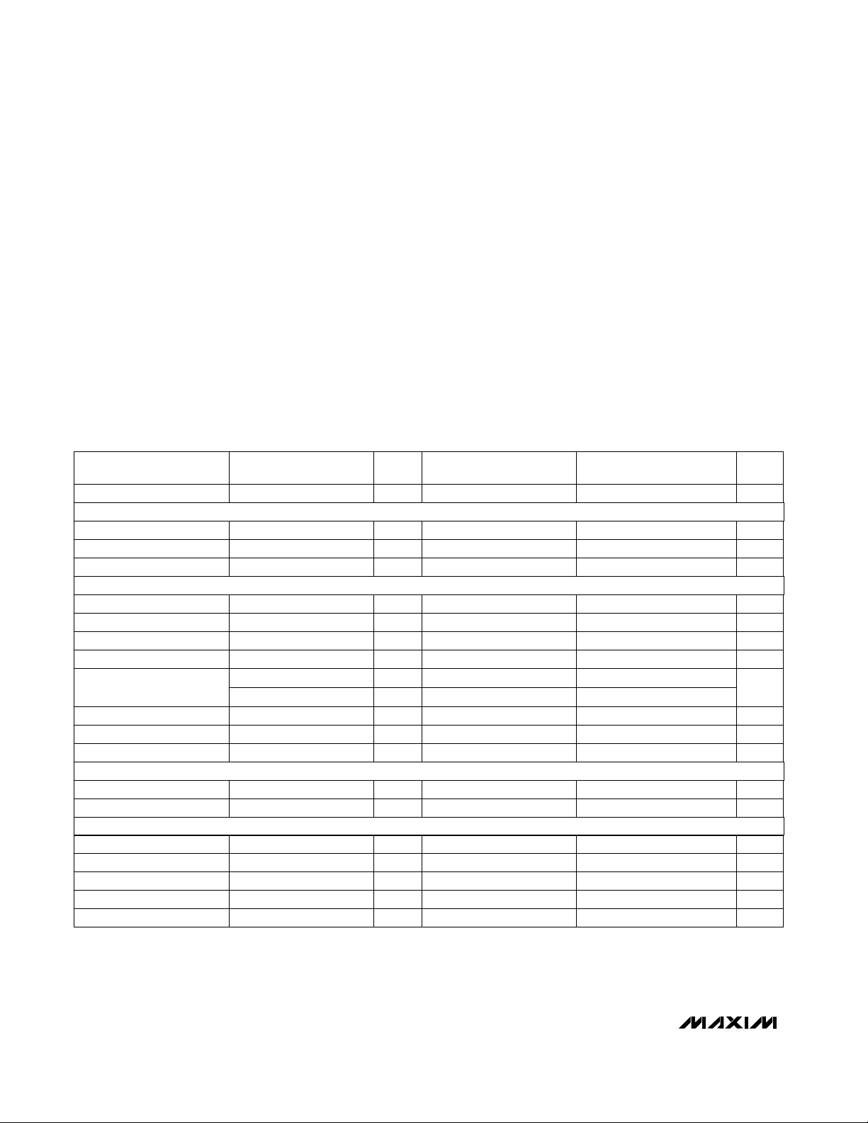
ELECTRICAL CHARACTERISTICS
(VEE= -5.2V, V
= TC= TA= +25°C.) (Note 1)
T
j
DC ACCURACY
Integral Nonlinearity
ANALOG INPUT
Input Voltage Range
Input Capacitance
Input Bandwidth
REFERENCE INPUT
TIMING CHARACTERISTICS
CLK to DATA READY Delay
= -2.00V, VRM= -1.00V, VRT= 0.00V, f
RB
CONDITIONSPARAMETER
= 100kHz
CLK
= 100kHzDifferential Nonlinearity
CLK
Small signal
Large signal V 500 500
RT
RB
= 750MHz, duty cycle = 50%, typical thermal impedance (θJC) = 4°C/W,
CLK
TEST
LEVEL
I
I
I
I
V
V
V
IV
IV mV-30 30Offset Error V
V V/ns5Input Slew Rate 5
I
V
I
V
V
IV
IV
Digital Output Current ...........................................0mA to -28mA
Operating Temperature Range ...........................-20°C to +85°C
Case Temperature...........................................................+125°C
Junction Temperature......................................................+150°C
Lead Temperature (soldering, 10sec).............................+300°C
Storage Temperature Range.............................-65°C to +150°C
MAX1151A
MIN TYP MAX
GuaranteedNo Missing Codes
RB
900
V
RT
MAX1151B
MIN TYP MAX
8
-1.5 1.5
-0.95 1.5
Guaranteed
V
RB
0.75 2.0
15
15
900
-30 30
-30 30
60 80
30
750
2
250
0.9 1.4 1.9
1.25 1.75 2.25
V
UNITS
RT
Bits8Resolution
LSB-1.0 1.0f
LSB-0.85 0.95f
VV
mA0.75 2.0VIN= 0VInput Bias Current
kΩ15Input Resistance
pF15Over full input range
MHz
mV-30 30Offset Error V
Ω60 80Ladder Resistance
MHz30Reference Bandwidth
MHz750Maximum Sample Rate
ps2Aperture Jitter
ps250Acquisition Time
ns0.9 1.4 1.9
ns1.25 1.75 2.25Clock to Data Delay
2 _______________________________________________________________________________________
8-Bit, 750Msps Flash ADC
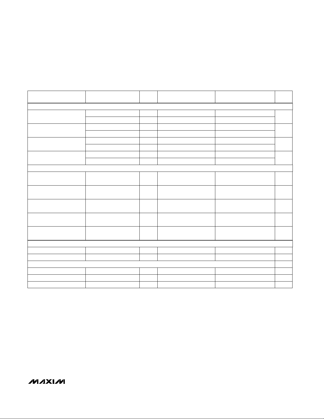
ELECTRICAL CHARACTERISTICS (continued)
(VEE= -5.2V, V
= TC= TA= +25°C.) (Note 1)
T
j
DYNAMIC PERFORMANCE
Signal-to-Noise Ratio
(without harmonics)
Total Harmonic Distortion
Signal-to-Noise and
Distortion
Spurious-Free Dynamic
Range
DIGITAL INPUTS
Input High Voltage
(CLK, NCLK)
Input Low Voltage
(CLK, NCLK)
Clock Pulse Width High
(t
)
PWH
Clock Pulse Width Low
(t
)
PWL
Clock Synchronous
Input Currents
DIGITAL OUTPUTS
POWER-SUPPLY REQUIREMENTS
= -2.00V, VRM= -1.00V, VRT= 0.00V, f
RB
CONDITIONSPARAMETER
fIN= 250MHz
= 750MHz, duty cycle = 50%, typical thermal impedance (θJC) = 4°C/W,
CLK
TEST
LEVEL
I
I
I
I
I
I
I
I
I
I
I 0.67 0.5 0.67 0.5 ns
V µA2
I
I
V
IV
I
I W5.5 6.25Power Dissipation 5.5 6.25
MAX1151A
MIN TYP MAX
46fIN= 50MHz
44
-45fIN= 50MHz
-37fIN= 250MHz
43fIN= 50MHz
48fIN= 50MHz
40fIN= 250MHz
2.4
MAX1151B
MIN TYP MAX
44
42
-43
-35
41
3436IfIN= 250MHz
44
36
-1.1 -0.7
-1.8 -1.5
0.67 0.5
2
-1.1 -0.9
-1.8 -1.5
2.4
-4.95 -5.2 -5.45
1.05 1.2
MAX1151
UNITS
dB
dBc
dB
dB
V-1.1 -0.7
V-1.8 -1.5
ns0.67 0.5
V-1.1 -0.9Logic "1" Voltage
V-1.8 -1.5Logic "0" Voltage
V-4.95 -5.2 -5.45Supply Voltage (VEE)
A1.05 1.2Supply Current (IEE)
Note 1: All parameters having min/max specifications are guaranteed. The Test Level column indicates the specific device testing actually
performed during production and Quality Assurance inspection. Unless otherwise noted, all tests are pulsed tests; therefore,
= TC = TA.
T
j
TEST LEVEL
I
II
III
IV
V
VI
TEST PROCEDURE
100% production tested at the specified temperature.
100% production tested at T
QA sample tested only at the specified temperatures.
Parameter is guaranteed (but not tested) by design and characterization data.
Parameter is a typical value for information purposes only.
100% production tested at T
_______________________________________________________________________________________ 3
= +25°C, and sample tested at the specified temperatures.
A
= +25°C. Parameter is guaranteed over specified temperature range.
A

8-Bit, 750Msps Flash ADC
______________________________________________________________Pin Description
PIN
1, 2, 3 D2B, D3B, D4B Data Output Bank, Bits 2, 3, and 4
4, 5, 19, 20, 22, 23, 27, 28, 38, 39,
40, 46, 47, 49, 60, 67, 79
6 D5B Data Output Bank B, Bit 5
MAX1151
7, 9, 11, 54, 56, 58,
69, 71, 73, 75, 77
8 D6B Data Output Bank B, Bit 6
10 D7B Data Output Bank B, Bit 7 (MSB)
12 D8B Data Output Bank B, Bit 8 (OVR)
13, 14, 31, 34, 41, 63, 64 N.C. No Connection. Not internally connected.
15-18, 25, 26, 29, 30, 36,
37, 44, 45, 51, 52
21 VRBF Reference-Voltage Force Bottom
24 VRBS Reference-Voltage Sense Bottom
32, 33 VIN Analog Input Voltage. Can be either voltage or sense.
35 VRM Reference-Voltage Middle, nominally -1V
42 VRTF Reference-Voltage Force Top
43 VRTS Reference-Voltage Sense Top
48 NCLK Inverse Clock Input
50 CLK Clock Input
53 DRA Data Ready Bank A
55 NDRA Not Data Ready Bank A
57 D0A Data Output Bank A, Bit 0 (LSB)
59, 61, 62, 65, 66, 68 D1A–D6A Data Output Bank A, Bits 1–6
70 D7A Data Output Bank A, Bit 7 (MSB)
72 D8A Data Output Bank A, Bit 8 (OVR)
74 NDRB Not Data Ready Bank B
76 DRB Data Ready Bank B
78 D0B Data Output Bank B, Bit 0 (LSB)
80 D1B Data Output Bank B, Bit 1
NAME FUNCTION
V
EE
DGND Digital Ground
AGND Analog Ground
Negative Supply, nominally -5.2V
_______________Detailed Description
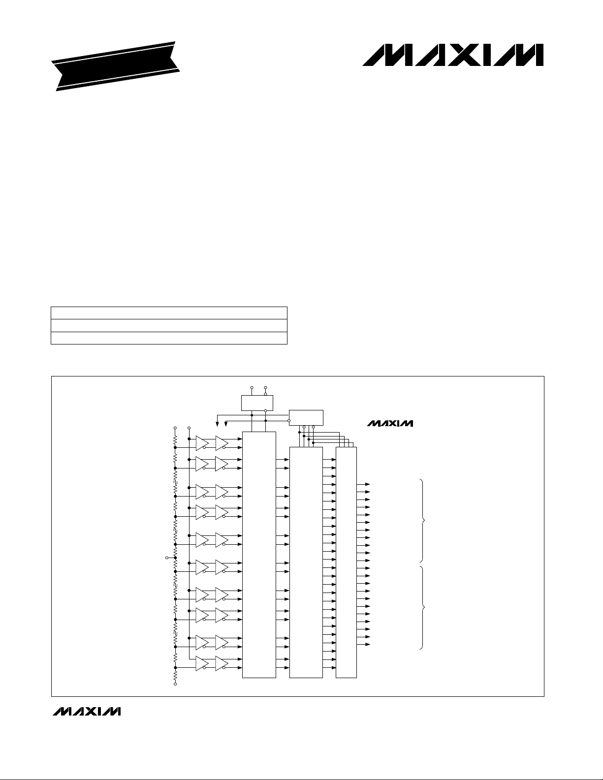
The MAX1151 is one of the fastest monolithic, 8-bit, parallel, flash analog-to-digital converters (ADCs) available
today. The nominal conversion rate is 750Msps, and the
analog bandwidth is in excess of 900MHz. A major
advance over previous flash converters is the inclusion of
255 input preamplifiers between the reference ladder and
input comparators (see
only reduces clock transient kickback to the input and
reference ladder but also reduces the effect of the input
4 _______________________________________________________________________________________
Functional Diagram
). This not
signal’s dynamic state on the input comparators’ latching
characteristics. The preamplifiers act as buffers to stabilize the input capacitance so that it remains constant over
different input voltage and frequency ranges, making the
part easier to drive than previous flash converters. The
preamplifiers also add a gain of +2 to the input signal, so
that each comparator has a wider overdrive or threshold
range to trip into or out of the active state. This gain
reduces metastable states that can cause errors at the
output.

8-Bit, 750Msps Flash ADC
The MAX1151 has true differential analog and digital
data paths from the preamplifiers to the output buffers
(current-mode logic) for reducing potential missing
codes while rejecting common-mode noise.
Signature errors are also reduced by careful layout of the
analog circuitry. The device’s output drive capability can
provide full ECL swings into 50Ωloads.
Typical Interface Circuit
The circuit of Figure 1 shows a method of achieving the
least error by correcting for integral linearity, inputinduced distortion, and power-supply/ground noise. This
is achieved with the use of external reference-ladder tap
connections, an input buffer, and supply decoupling.
Contact the factory for the MAX1150/MAX1151 evaluation kit manual, which contains more details on interfacing the MAX1151. The function of each pin and external
connections to other components are described in the following sections.
VEE, AGND, DGND
VEEis the supply pin with AGND as ground for the
device. The power-supply pins should be bypassed as
close to the device as possible with at least a 0.01µF
ceramic capacitor. A 1µF tantalum can also be used for
low-frequency suppression. DGND is the ground for the
ECL outputs, and should be referenced to the output
pulldown voltage and appropriately bypassed, as shown
in Figure 1.
VIN (Analog Input)
There are two analog input pins that are tied to the same
point internally. Either one may be used as an analog
input sense, while the other is used for input force. This is
convenient for testing the source signal to see if there is
sufficient drive capability. The pins can also be tied together and driven by the same source. The MAX1151 is
superior to similar devices due to a preamplifier stage
before the comparators. This makes the device easier to
drive because it has constant capacitance and induces
less slew-rate distortion.
CLK, NCLK (Clock Inputs)
The clock inputs are designed to be driven differentially
with ECL levels. The duty cycle of the clock should be
kept at 50%, to avoid causing larger second harmonics.
If this is not important to the intended application, duty
cycles other than 50% may be used.
D0 to D8, DR, NDR (A and B)
The digital outputs can drive 50Ω to ECL levels when
pulled down to -2V. When pulled down to -5.2V, the outputs can drive 130Ω to 1kΩ loads. All digital outputs are
gray code, with the coding as shown in Table 1.
Table 1. Output Coding
V
(V) D8 D7 . . . D0
IN
0
-0.5
-1.0
-1.5
-2.0
There are two reference inputs and one external reference voltage tap. These are -2V (VRB force and sense),
mid-tap (VRM), and AGND (VRT force and sense). The
reference pins and tap can be driven by op amps (as
shown in Figure 1), or VRM can be bypassed for limited
temperature operation. These voltage inputs can be bypassed to AGND for further noise suppression, if
desired.
The typical thermal impedance (θCA) for the MQUAD
package has been measured at θ
air with no heatsink.
To ensure rated performance, we highly recommend
using this device with a heatsink that can provide adequate air flow. We have found that a Thermalloy 17846
heatsink with a minimum air flow of 1 meter/second
(200 linear feet per minute) provides adequate thermal
performance under laboratory tests. Application-specific conditions should be taken into account to ensure
that the device is properly heat sinked.
1
0
0
0
0
10000000
10000001
10000011
•
•
•
10100001
10100000
11100000
•
•
•
11000001
11000000
01000000
•
•
•
01100001
01100000
00100000
•
•
•
00000011
00000001
00000000
VRBF, VRBS, VRTF, VRTS, VRM
(Reference Inputs)
Thermal Management
CA
= 17°C/W, in still
MAX1151
_______________________________________________________________________________________ 5

8-Bit, 750Msps Flash ADC
V
IN
MAX1151
-2.0V
REFERENCE
50Ω
R
U1
R
U1
22Ω
22Ω
1N2907
-5.2V
VIN
VIN
VRTF
VRTS
VRM
**
VRBS
VRBF
**
MAX1151
NDRB (NOT DATA READY)
DRB (DATA READY)
D8B (OVR)
D7B (MSB)
D6B
D5B
D4B
D3B
D2B
D1B
D0B (LSB)
NDRA (NOT DATA READY)
DRA (DATA READY)
D8A (OVR)
D7A (MSB)
D6A
D5A
D4A
D3A
D2A
D1A
D0A (LSB)
BANK B
BANK A
0.1µF
***********
***********
-2.0V
PULL-DOWN
(DIGITAL)
CLOCK IN
U2
50Ω 50Ω
-2V
PULL-DOWN
(ANALOG)
CLK
NCLK
V
-5.2V
EE
AGND
**
DGND
L =
Ferrite bead, DIGIKEY P98208BK or equivalent
L
* =
50Ω resistor
* * =
10µF tantalum capacitor and 0.1µF chip capacitor
U1 =
OP220 or equivalent with low offset/noise
R =
1kΩ; 0.1% matched
=
AGND
=
DGND
U2 =
Motorola ECLinPS Lite, MC10EL16, differential receiver
with 250ps (typ) propagation delay
Figure 1. Typical Interface Circuit
6 _______________________________________________________________________________________

8-Bit, 500Msps Flash ADC
Operation
The MAX1151 has 255 preamplifier/comparator pairs;
each is supplied with the voltage from VRT to VRB,
divided equally by the resistive ladder as shown in the
Functional Diagram
tive input of each preamplifier/comparator pair. An analog input voltage applied at VIN is connected to the
negative inputs of each preamplifier/comparator pair.
The comparators are then clocked through each one’s
individual clock buffer. When the CLK pin is in the low
state, the master or input stage of the comparators
compares the analog input voltage to the respective
reference voltage. When CLK changes from low to
high, the comparators are latched to the state prior to
the clock transition and output logic codes in sequence
from the top comparators, closest to VRT (0V), down to
the point where the magnitude of the input signal
changes sign (thermometer code). The output of each
comparator is then registered into four 64-to-6 bit decoders when CLK is changed from high to low. At the
output of the decoders is a set of four 7-bit latches that
are enabled (track) when the clock changes from high
to low. From here, the output of the latches is coded
into six LSBs from four columns, and four columns are
coded into two MSBs. Finally, eight ECL output latches
and buffers are used to drive the external loads. The
conversion takes one clock cycle from the input to the
data outputs.
. This voltage is applied to the posi-
VIN
CLK
NCLK
DRA
NDRA
DATA BANK A
DRB
NDRB
DATA BANK B
N
N + 1
1.3ns
1.4ns
TYP
N - 2 N N + 2
N + 2
1.75ns
TYP
1.4ns
TYP
N + 3
N - 1
1.75ns
TYP
Figure 2. Timing Diagram
N + 4
N + 1 N + 3
N + 5
MAX1151
N + 6
N + 7
N + 4
INPUT CIRCUIT
AGND
VIN
V
EE
Figure 3. Subcircuit Schematics
_______________________________________________________________________________________ 7
CLOCK INPUTOUTPUT CIRCUIT
AGND
AGND DGND
V
R
DATA OUT
CLK NCLK
V
EE

8-Bit, 750Msps Flash ADC
____________________________________________________________Pin Configuration
TOP VIEW
MAX1151
D2B
D3B
D4B
V
V
D5B
DGND
D6B
DGND
D7B
DGND
D8B
N.C.
N.C.
AGND
AGND
AGND
AGND
V
V
V
RBF
V
V
V
RBS
EE
D1B
V
80
79
1
2
3
4
EE
5
EE
6
7
8
9
10
11
12
13
14
15
16
17
18
19
EE
20
EE
21
22
EE
23
EE
24
D0B
78
DGND
77
DRB
76
DGND
75
DGND
NDRB
73
74
MAX1151
D8A
72
DGND
71
D7A
70
DGND
69
D6A
68
EE
D4A
D5A
V
65
66
67
64 N.C.
N.C.
63
D3A
62
D2A
61
V
60
EE
D1A
59
DGND
58
D0A
57
DGND
56
NDRA
55
DGND
54
DRA
53
AGND
52
AGND
51
CLK
50
V
49
EE
NCLK
48
V
47
EE
V
46
EE
AGND
45
AGND
44
VRTS
43
VRTF
42
N.C.
41
25
AGND
26
AGND
32
EE
V
V
AGND
AGND
N.C.
VIN
31
30
29
28
27
EE
33
VIN
34
N.C.
35
VRM
36
AGND
37
AGND
39
38
V
40
EE
EE
EE
V
V
MQUAD
Maxim cannot assume responsibility for use of any circuitry other than circuitry entirely embodied in a Maxim product. No circuit patent licenses are
Maxim cannot assume responsibility for use of any circuitry other than circuitry entirely embodied in a Maxim product. No circuit patent licenses are
implied. Maxim reserves the right to change the circuitry and specifications without notice at any time.
implied. Maxim reserves the right to change the circuitry and specifications without notice at any time.
8
___________________Maxim Integrated Products, 120 San Gabriel Drive, Sunnyvale, CA 94086 (408) 737-7600
8
___________________Maxim Integrated Products, 120 San Gabriel Drive, Sunnyvale, CA 94086 (408) 737-7600
© 1996 Maxim Integrated Products Printed USA is a registered trademark of Maxim Integrated Products.
© 1996 Maxim Integrated Products Printed USA is a registered trademark of Maxim Integrated Products.
 Loading...