

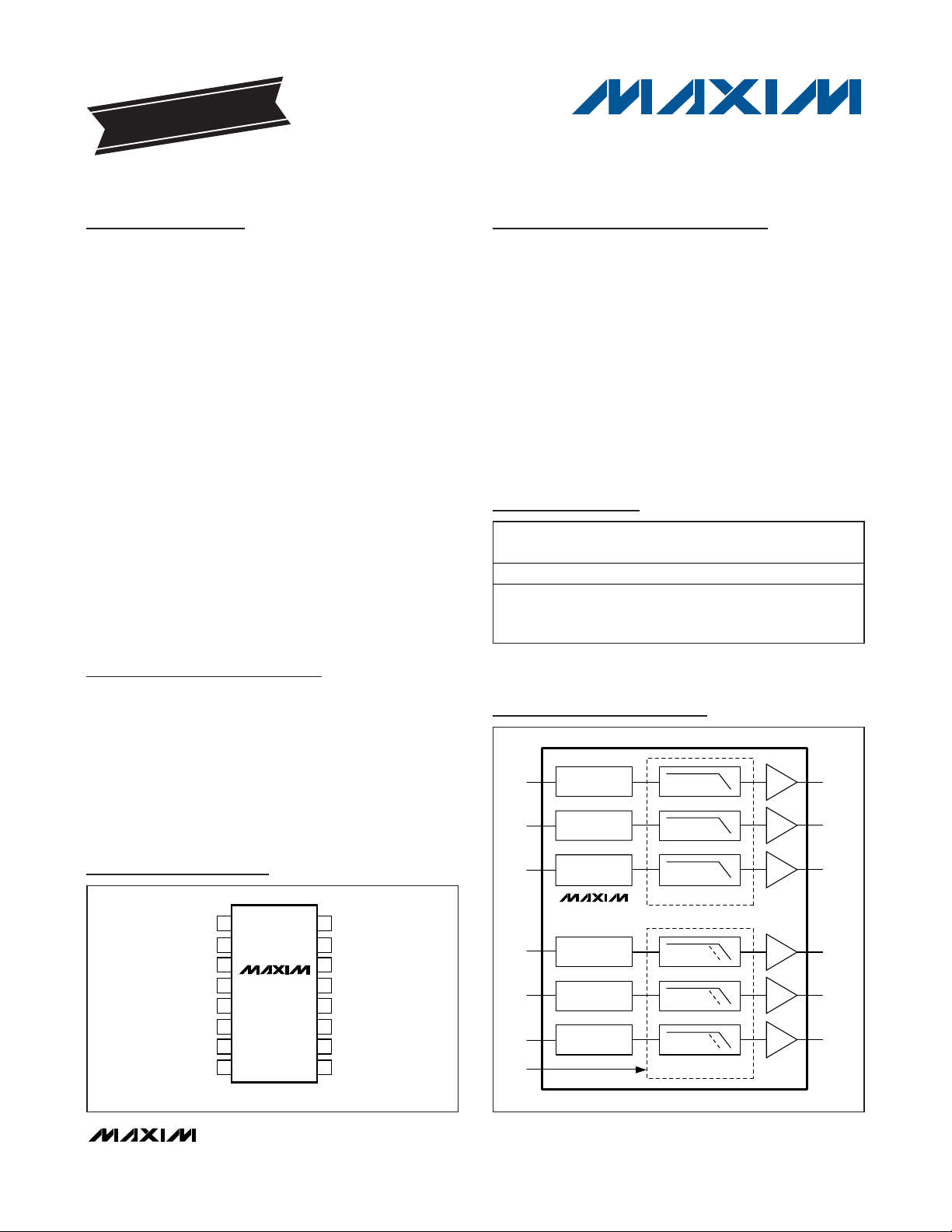
General Description
The MAX11506/MAX11507 integrated filters offer six
channels, three for standard-definition (SD) video and
three for either SD or high-definition (HD) video, and
include +6dB output buffers on each channel. These
video filters are ideal for anti-aliasing and DAC smoothing in applications such as set-top boxes, digital video
recorders, DVD players, and personal video recorders.
The MAX11506/MAX11507 video inputs feature a transparent clamp compatible with AC- and DC-coupled input
signals and allow DAC outputs to be directly coupled. The
filters provide -3dB bandwidth of 9.0MHz for the SD filters
and 33MHz for the HD filters. Each channel includes an
output buffer with a gain of +6dB capable of driving a full
2V
P-P
video signal into a 150Ω video load. The buffers
drive either AC- or DC-coupled loads and assure a blanking level of below 1V after the backmatch resistor. DCcoupling eliminates bulky coupling capacitors.
The MAX11506 offers a flat passband while the
MAX11507 features 0.8dB peaking on the three SD-only
channels to compensate for system roll-off. The
MAX11506/MAX11507 operate from a single +5V supply
and are available in the 0°C to +70°C commercial temperature grade. The MAX11506/MAX11507 are offered in
the 16-pin QSOP package.
Applications
Cable and Satellite Set-Top Box Receivers
HDTVs
DVD Players
Personal Video Recorders
Digital Video Recorders (DVRs)
SDTVs
Video On-Demand
HD Recorders
Features
♦ Three Selectable 6th-Order 9MHz/33MHz
(SD/HD) Filters
♦ Three Fixed 5th-Order 9MHz (SD) Filters
♦ +6dB Output Buffers
♦ Transparent Input Clamp
♦ AC- or DC-Coupled Inputs
♦ AC- or DC-Coupled Outputs
♦ 0.8dB Peaking Passband Response
(MAX11507) on Three SD-Only Channels
♦ Output Buffers Drive a Standard 150Ω Video
Load
♦ Single +5V Power Supply
♦ Lead-Free 16-Pin QSOP Package
MAX11506/MAX11507
Low-Cost, 6-Channel SD Plus HD/SD
Selectable Video Filters and Buffers
________________________________________________________________
Maxim Integrated Products
1
Pin Configuration
19-4122; Rev 0; 4/08
For pricing, delivery, and ordering information, please contact Maxim Direct at 1-888-629-4642,
or visit Maxim’s website at www.maxim-ic.com.
EVALUATION KIT
AVAILABLE
Typical Operating Circuit appears at end of data sheet.
Ordering Information
+
Denotes a lead-free package.
PART
TEMP RANGE
PIN-
FREQUENCY
RESPONSE
MAX11506CEE+
Flat
MAX11507CEE+
High
Frequency
Boost
SD/HDOUT1
SD/HDIN1
SD/HDOUT2
SD/HDIN2
SD/HDOUT3
SD/HDIN3
SDOUT1SDIN1
SDOUT2SDIN2
SDOUT3SDIN3
FSEL
TRANSPARENT
CLAMP
TRANSPARENT
CLAMP
TRANSPARENT
CLAMP
TRANSPARENT
CLAMP
TRANSPARENT
CLAMP
TRANSPARENT
CLAMP
9MHz, 5TH ORDER
9MHz/33MHz, 6TH ORDER
MAX11506
MAX11507
6dB
6dB
6dB
6dB
6dB
6dB
Block Diagram
PACKAGE
0°C to +70°C 16 QSOP
0°C to +70°C 16 QSOP
TOP VIEW
SDIN1
SDIN2
SDIN3
SD/HDIN1
SD/HDIN2
SD/HDIN3
+
1
2
3
MAX11506
4
V
CC
5
6
7
8
MAX11507
QSOP
FSEL
16
SDOUT1
15
SDOUT2
14
SDOUT3
13
GND
12
GND
SD/HDOUT1
11
10
SD/HDOUT2
9
SD/HDOUT3
MAX11506/MAX11507
Low-Cost, 6-Channel SD Plus HD/SD
Selectable Video Filters and Buffers
2 _______________________________________________________________________________________
ABSOLUTE MAXIMUM RATINGS
DC ELECTRICAL CHARACTERISTICS
(VCC= +5V, R
LOAD
= 150Ω to GND, CIN= 0.1µF, TA= 0°C to +70°C, unless otherwise noted.)
Stresses beyond those listed under “Absolute Maximum Ratings” may cause permanent damage to the device. These are stress ratings only, and functional
operation of the device at these or any other conditions beyond those indicated in the operational sections of the specifications is not implied. Exposure to
absolute maximum rating conditions for extended periods may affect device reliability.
VCCto GND............................................................. -0.3V to +6V
All Other Pins
to GND ................-0.3V to the lower of (V
CC
+ 0.3V) and +6V
Continuous Power Dissipation (T
A
= +70°C)
16-Pin QSOP (derate 9.6mW/°C above +70°C)....... 771.5mW
Maximum Current into Any Pin except V
CC
and GND .....±50mA
Operating Temperature Range...............................0°C to +70°C
Storage Temperature Range .............................-65°C to +150°C
Lead Temperature (soldering, 10s) .................................+300°C
Junction Temperature......................................................+150°C
AC ELECTRICAL CHARACTERISTICS
(VCC= +5V, R
LOAD
= 150Ω to GND, CIN= 0.1µF, TA= 0°C to +70°C, frequency response relative to 100kHz, unless otherwise
noted.)
PARAMETER SYMBOL CONDITIONS MIN TYP MAX UNITS
Supply Current I
Supply Voltage Range V
Input-Voltage Range V
Digital Input High Voltage V
Digital Input Low Voltage V
CC
CC
IN
IH
IL
4.75 5.00 5.25 V
2.0 V
40 61 mA
1.4 V
0.8 V
PARAMETER SYMBOL CONDITIONS MIN TYP MAX UNITS
STANDARD-DEFINITION VIDEO
-1dB Bandwidth f
-3dB Bandwidth f
Stopband Attenuation A
Low-Frequency Gain A
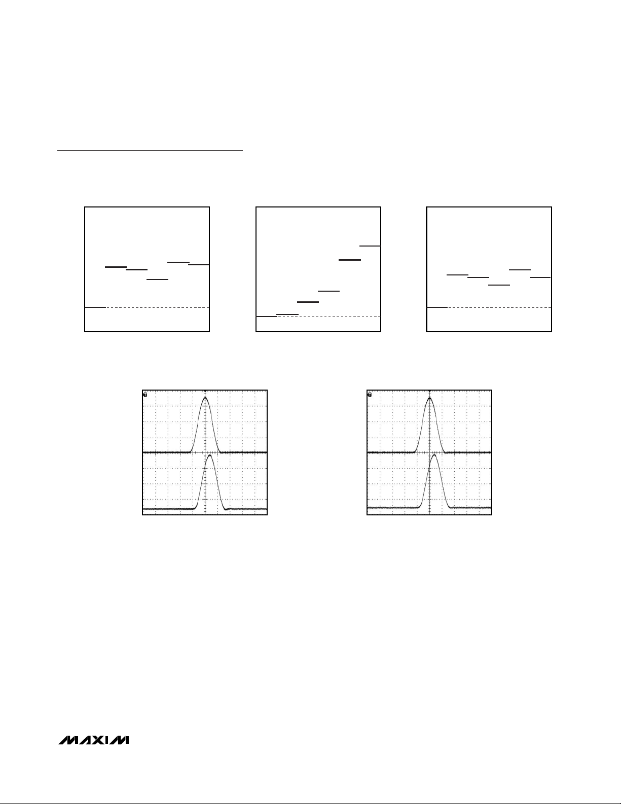
Differential Gain dG All channels 0.5 %
Differential Phase dφ All channels 0.2 Degrees
Total Harmonic Distortion THD V
Channel-to-Channel Crosstalk X
Signal-to-Noise Ratio SNR Peak signal (2V
Propagation Delay t
Power-Supply Rejection Ratio PSRR DC (all channels) 45 dB
MAX11506, SD 4.5 7.9
1dB
3dB
TALK
PD
MAX11506, SD/HD in SD mode 4.5 7.9
MAX11507, SD 5.0 8.6
MAX11507, SD/HD in SD mode 4.5 7.9
9.0 MHz
f = 27MHz 48 dB
SB
No load 5.8 6.0 6.2 dB
V
= 1.4V
OUT
f = 1MHz -60 dB
f = 4.5MHz 59 ns
, f = 1MHz (all channels) 0.1 %
P-P
) to RMS noise, 100kHz, 4.2MHz 71 dB
P-P
MHz
MAX11506/MAX11507
Low-Cost, 6-Channel SD Plus HD/SD
Selectable Video Filters and Buffers
_______________________________________________________________________________________ 3
AC ELECTRICAL CHARACTERISTICS (continued)
(VCC= +5V, R
LOAD
= 150Ω to GND, CIN= 0.1µF, TA= 0°C to +70°C, frequency response relative to 100kHz, unless otherwise
noted.)
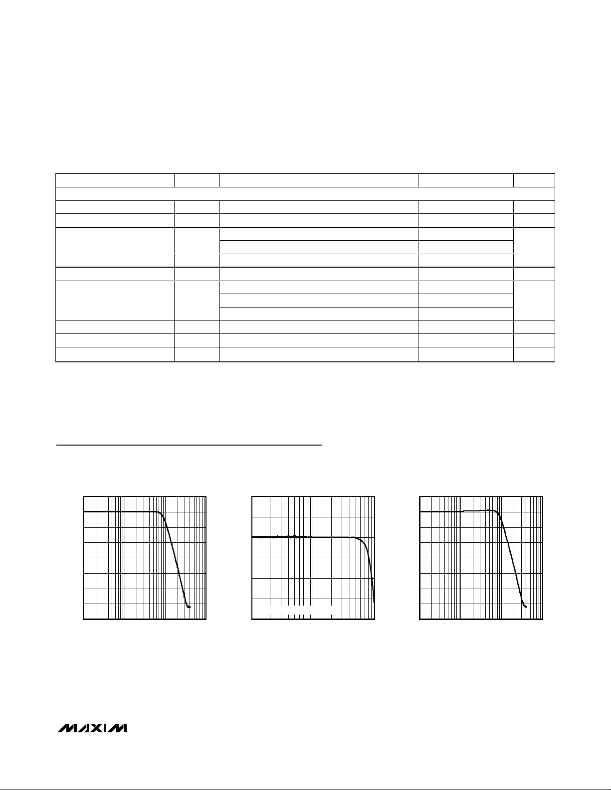
Typical Operating Characteristics
(VCC= 5V, RL= 150Ω to GND, output DC-coupled, TA= +25°C.)
PARAMETER SYMBOL CONDITIONS MIN TYP MAX UNITS
HIGH-DEFINITION VIDEO
-1dB Bandwidth f
-3dB Bandwidth f
Stopband Attenuation A
Low-Frequency Gain A
Total Harmonic Distortion THD
Channel-to-Channel Crosstalk X
Signal-to-Noise Ratio SNR Peak signal (2V
Group-Delay Deviation ∆t
1dB
3dB
TA = +25°C 23 30 MHz
f = 37.125MHz 4.0
f = 44.250MHz 13
SB
f = 74.250MHz, TA = +25°C 32.0 46.0
V
V
TALK
g
= 1.4V
OUT
V
= 1.4V
OUT
V
= 1.4V
OUT
f = 1MHz -60 dB
f = 100kHz to 26MHz 15 ns
, f = 10MHz 0.4
P-P
, f = 15MHz 0.4
P-P
, f = 22MHz 0.6
P-P
) to RMS noise, 100kHz, 30MHz 65 dB
P-P
33 MHz
dB
5.8 6.0 6.2 dB
%
MAX11506 FREQUENCY RESPONSE
MAX11506 PASSBAND RESPONSE
SD CHANNEL
10
0
-10
-20
-30
-40
NORMALIZED GAIN (dB)
-50
-60
-70
0.1 100
FREQUENCY (MHz)
101
MAX11506 toc01
4
2
0
-2
-4
NORMALIZED GAIN (dB)
-6
NORMALIZED TO ZERO AT 100kHz
-8
0.1 10
SD CHANNEL
1
FREQUENCY (MHz)
10
MAX11506 toc02
0
-10
-20
-30
-40
NORMALIZED GAIN (dB)
-50
-60
-70
MAX11507 FREQUENCY RESPONSE
0.1 100
SD CHANNEL
FREQUENCY (MHz)
MAX11506 toc03
101
MAX11506/MAX11507
Low-Cost, 6-Channel SD Plus HD/SD
Selectable Video Filters and Buffers
4 _______________________________________________________________________________________
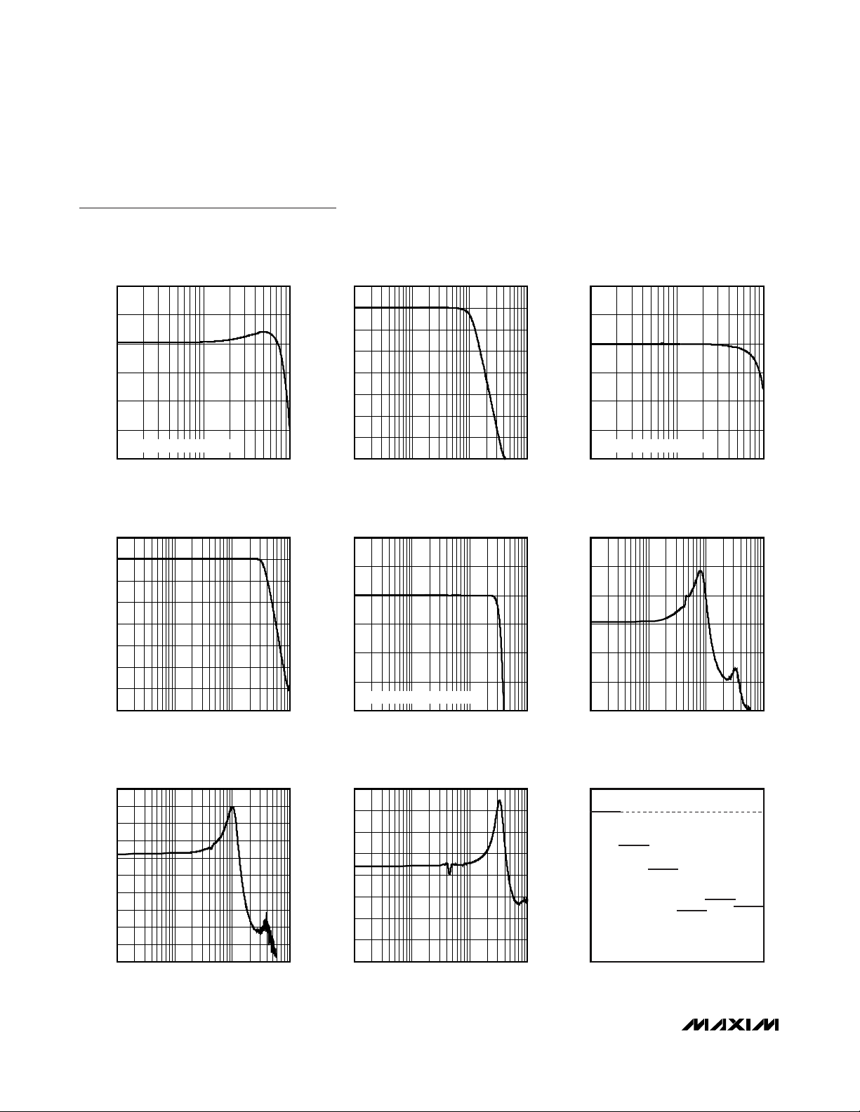
Typical Operating Characteristics (continued)
(VCC= 5V, RL= 150Ω to GND, output DC-coupled, TA= +25°C.)
MAX11507 PASSBAND RESPONSE
SD CHANNEL
4
2
0
-2
-4
NORMALIZED GAIN (dB)
-6
NORMALIZED TO ZERO AT 100kHz
-8
0.1 10
1
FREQUENCY (MHz)
10
MAX11506 toc04
0
-10
-20
-30
-40
NORMALIZED GAIN (dB)
-50
-60
-70
0.1 100
FREQUENCY RESPONSE
-10
-20
-30
-40
NORMALIZED GAIN (dB)
-50
-60
-70
SD/HD CHANNEL IN HD MODE
10
0
0.1 100
FREQUENCY (MHz)
101
4
MAX11506 toc07
2
0
-2
-4
NORMALIZED GAIN (dB)
-6
-8
NORMALIZED TO ZERO AT 100kHz
0.1 10 100
FREQUENCY RESPONSE
SD/HD CHANNEL IN SD MODE
101
FREQUENCY (MHz)
PASSBAND RESPONSE
SD/HD CHANNEL IN HD MODE
1
FREQUENCY (MHz)
4
MAX11506 toc05
MAX11506 toc08
2
0
-2
-4
NORMALIZED GAIN (dB)
-6
-8
120
100
80
60
DELAY (ns)
40
20
0
PASSBAND RESPONSE
SD/HD CHANNEL IN SD MODE
NORMALIZED TO ZERO AT 100kHz
0.1 10
1
FREQUENCY (MHz)
GROUP DELAY vs. FREQUENCY
SD CHANNEL
0.1 10 100
1
FREQUENCY (MHz)
MAX11506 toc06
MAX11506 toc09
GROUP DELAY vs. FREQUENCY
SD/HD CHANNEL IN SD MODE
100
90
80
70
60
50
DELAY (ns)
40
30
20
10
0
0.1 10 100
1
FREQUENCY (MHz)
MAX11506 toc10
GROUP DELAY vs. FREQUENCY
SD/HD CHANNEL IN HD MODE
40
35
30
25
20
DELAY (ns)
15
10
5
0
0.1 10 100
1
FREQUENCY (MHz)
1.0
MAX11506 toc11
-0.1
-0.2
-0.3
-0.4
DIFFERENTIAL GAIN (%)
-0.5
-0.6
-0.7
DIFFERENTIAL GAIN, NTSC
SD CHANNEL
0
2
134567
MAX11506 toc12
STEP
MAX11506/MAX11507
Low-Cost, 6-Channel SD Plus HD/SD
Selectable Video Filters and Buffers
_______________________________________________________________________________________
5
Typical Operating Characteristics (continued)
(VCC= 5V, RL= 150Ω to GND, output DC-coupled, TA= +25°C.)
DIFFERENTIAL PHASE, NTSC
SD CHANNEL
0.4
0.3
0.2
0.1
DIFFERENTIAL PHASE (deg)
0
-1.0
2
134657
STEP
2T RESPONSE
SD CHANNEL
0.7
0.6
MAX11506 toc13
0.5
0.4
0.3
0.2
DIFFERENTIAL GAIN (%)
0.1
-1.0
MAX11506 toc16
DIFFERENTIAL GAIN, NTSC
SD/HD CHANNEL IN SD MODE
0
2
134567
INPUT
STEP
DIFFERENTIAL PHASE, NTSC
SD/HD CHANNEL IN SD MODE
0.4
MAX11506 toc14
0.3
0.2
0.1
DIFFERENTIAL PHASE (deg)
0
-1.0
2
134657
2T RESPONSE
SD/HD CHANNEL IN SD MODE
MAX11506 toc17
MAX11506 toc15
STEP
INPUT
200ns/div
OUTPUT
200ns/div
OUTPUT
MAX11506/MAX11507
Detailed Description
The MAX11506/MAX11507 integrated filters offer 6 channels, 3 for SD video and 3 for either SD or HD video and
include +6dB output buffers on each channel. Each
channel of the MAX11506/MAX11507 contains a transparent input clamp, a 9.0MHz 5th-order lowpass filter
and an output amplifier with a gain of 2V/V (see the
Typical Operating Circuit
). The MAX11506 provides a flat
passband response and the MAX11507 provides a
0.8dB high-frequency boost at 5MHz on all SD-only
channels to help with system roll-off. The SD-only channels add 280mV of offset at the output.
Three channels, SD/HD1, SD/HD2, and SD/HD3 include
selectable SD and HD video filters, each with a transparent input clamp, a 6th-order lowpass filter with a -3dB
bandwidth of 9.0MHz (SD) and 33MHz (HD), and an
output amplifier with a gain of 2V/V. The SD/HD channels add 550mV of offset at the output.
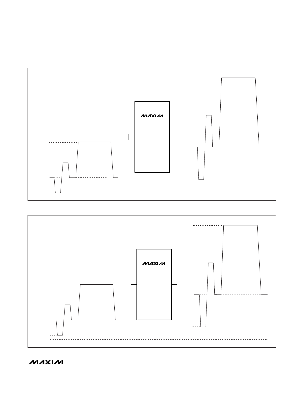
The output voltage equations are:
V
SDOUT
= (2 x VIN) + 0.28V
V
SD/HDOUT
= (2 x VIN) + 0.55V
Typical voltage waveforms are shown in Figures 1 and 2.
Inputs
Transparent Clamps
All inputs feature transparent clamps to allow either ACor DC-coupling of the inputs. The clamp remains inactive while the input signal is above ground, offering true
DC input coupling. When the signal goes below
ground, as is the case when it is AC-coupled, the
clamp sets the sync tip close to the ground level.
Input Coupling
The choice of AC- or DC-coupling the input depends
on the video source. Many DACs have a current output
and are terminated to ground with a resistor; such signals are conveniently DC-coupled. Use AC-coupling
when the DC level of the video signal is unknown or
outside the specified input range of the MAX11506/
MAX11507, such as SCART or VCC-terminated DAC
outputs.
DC-Coupled Inputs
When the input is DC-coupled, the voltage must remain
above zero but should not exceed 1.4V (typical).
Low-Cost, 6-Channel SD Plus HD/SD
Selectable Video Filters and Buffers
6 _______________________________________________________________________________________
Pin Description
PIN NAME FUNCTION
1 SDIN1 SD Video Input Channel 1
2 SDIN2 SD Video Input Channel 2
3 SDIN3 SD Video Input Channel 3
4VCCPower-Supply Input
5 FSEL
6 SD/HDIN1 SD/HD Video Input Channel 1
7 SD/HDIN2 SD/HD Video Input Channel 2
8 SD/HDIN3 SD/HD Video Input Channel 3
9 SD/HDOUT3 SD/HD Video Output Channel 3
10 SD/HDOUT2 SD/HD Video Output Channel 2
11 SD/HDOUT1 SD/HD Video Output Channel 1
12, 13 GND Ground
14 SDOUT3 SD Video Output Channel 3
15 SDOUT2 SD Video Output Channel 2
16 SDOUT1 SD Video Output Channel 1
Frequency-Select Input. SD/HD select for channels 4, 5, and 6. Force FSEL high to select HD, and
low to select SD. Do not leave unconnected.
MAX11506/MAX11507
Low-Cost, 6-Channel SD Plus HD/SD
Selectable Video Filters and Buffers
_______________________________________________________________________________________ 7
Figure 1. Typical AC-Coupled Signal
INPUT SIGNAL
0.32V
1.02V
0.02V
0.00V
OUTPUT SIGNAL
1.19V HD
0.98V SD
2.59V HD
2.32V SD
0.59V HD
0.32V SD
INPUT OUTPUT
MAX11506
MAX11507
Figure 2. Typical DC-Coupled Signal
1.0V
INPUT SIGNAL
0.3V
0.0V
MAX11506
MAX11507
INPUT OUTPUT
2.55V HD
2.28V SD
1.15V HD
0.88V SD
0.55V HD
0.28V SD
OUTPUT SIGNAL

MAX11506/MAX11507
Low-Cost, 6-Channel SD Plus HD/SD
Selectable Video Filters and Buffers
8 _______________________________________________________________________________________
AC-Coupled Inputs
When the input is AC-coupled, the transparent clamps
are active and set the lowest point of the signal at ground.
This is appropriate for unipolar signals such as CVBS, Y,
R, G, or B, with or without sync pulses (Figure 3).
For bipolar signals such as Pb and Pr, bias the AC-coupled inputs to a fixed DC voltage, typically 0.59V, to
ensure that the transparent clamp remains off. Figure 4
shows a typical network. Determine the bias voltage using:
where ILis the input leakage current (typically 0.5µA).
SD Filters
The MAX11506/MAX11507 filters are optimized to deliver a flat (MAX11506) or high-frequency boosted
(MAX11507) passband and high stopband attenuation.
The filter characteristic provides excellent time domain
response with low overshoot. The typical -3dB frequency of 9.0MHz guarantee minimal attenuation in the
passband, while at the same time offering a 27MHz
attenuation of typically -48dB.
HD Filters
The internal filters deliver a flat passband along with high
stopband attenuation. The filter characteristic provides
an excellent time domain response with low overshoot.
The typical -3dB frequency of 33MHz guarantees low
attenuation in the passband, while at the same time
allowing for a typical attenuation of -46dB at 74.25MHz.
Output Buffers
The MAX11506/MAX11507 feature output buffers with
+6dB gain that drive a standard 150Ω video load. A
typical load consists of a 75Ω backmatch resistor, an
optional 220µF or larger coupling capacitor, and a 75Ω
termination resistor. The offset between input and output signals ensures that the blanking level on the output
is less than 1V after the backmatch resistor, thus meeting digital TV specifications allowing the devices to
drive video loads directly without using costly AC-coupling
capacitors.
Applications Information
Output Considerations
The MAX11506/MAX11507 outputs may be DC- or ACcoupled. These devices, with +6dB gain, are typically
connected to a 75Ω series backmatch resistor followed
by the video cable. Choose an AC-coupling capacitor
value that ensures that the lowest frequency content in
the video signal is passed and the field-time distortion
is kept within desired limits when using an AC connection. The selection of this value is a function of the input
impedance, and more importantly, the input leakage of
the circuit being driven. Common industry practice is to
use a 220µF or larger capacitor.
Figure 3. Simple AC-Coupling for Unipolar Signals (CVBS, Y, R,
G, B)
INPUT
R1
820kΩ
R2
120kΩ
MAX11506
MAX11507
0.1µF
ENCODER
DAC
V
CC
Figure 4. AC-Coupling for Bipolar Signals (C, Pb, Pr)
R
V
BAVCCL
2
RR
+
12
xV I xR
()
()=
−
1
ENCODER
DAC
0.1µF
MAX11506
MAX11507
INPUT
MAX11506/MAX11507
Low-Cost, 6-Channel SD Plus HD/SD
Selectable Video Filters and Buffers
_______________________________________________________________________________________ 9
The MAX11506/MAX11507 outputs are fully protected
against short circuits to ground. The short-circuit protection circuitry limits the output current to 75mA (typical) per output. Shorting more than one output to
ground simultaneously may exceed the maximum
package power dissipation.
PCB Layout Recommendations
Connect the power and ground traces to large copper
areas to enhance power dissipation. Bypass VCCto
GND with 0.1µF and 1.0µF capacitors. Place the 0.1µF
capacitor closest to VCC. Use surface-mount capacitors
for their low inductance. Place traces carrying video
signals appropriately to avoid mutual coupling. When
inputs are AC-coupled, place the capacitors as close
as possible to the device and keep traces short to minimize parasitic capacitance and inductance. Refer to
the MAX11506/MAX11507 evaluation kit datasheet for
PCB layout.
Chip Information
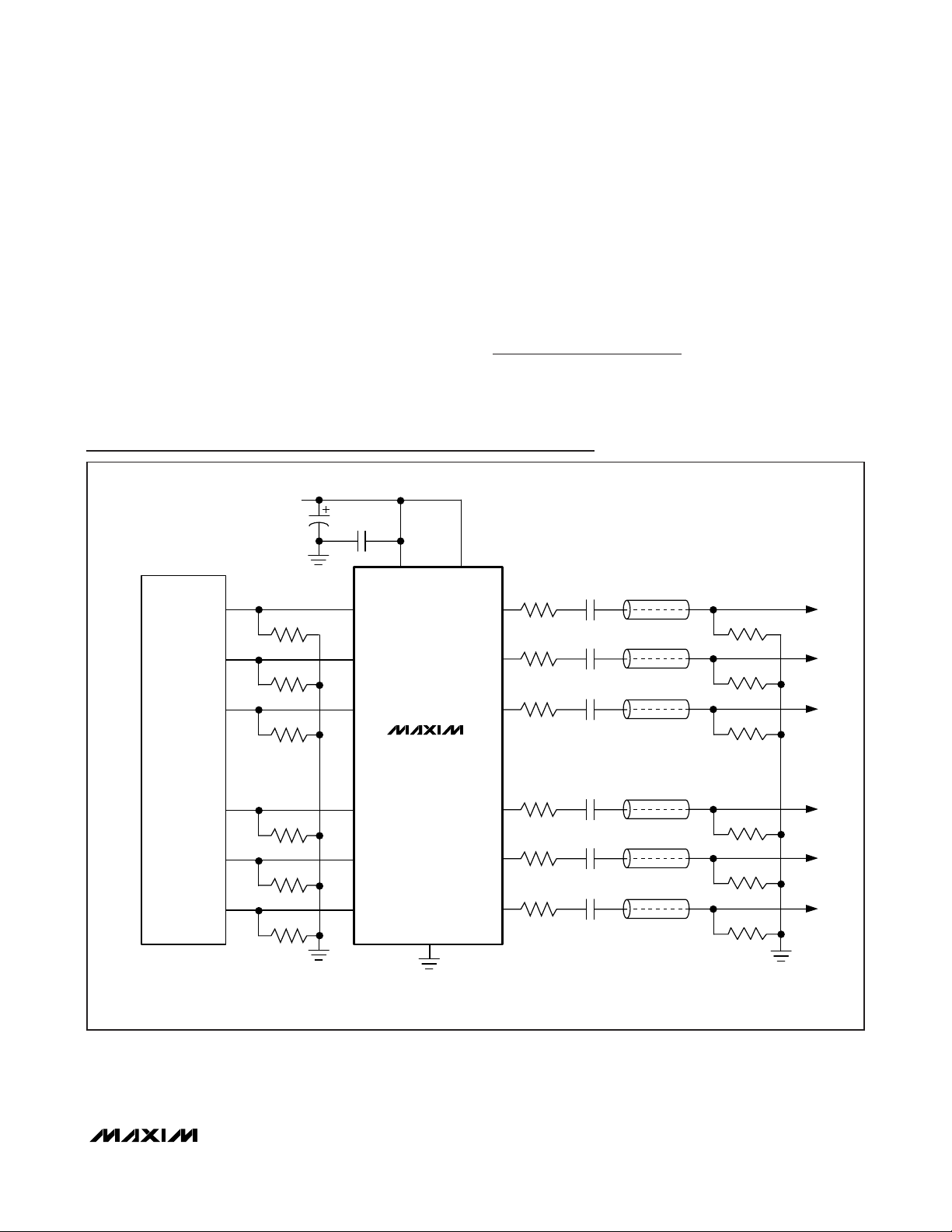
PROCESS: BiCMOS
VIDEO
SoC
Y1
OUT
C
OUT
CV
OUT
G/Y2
OUT
B/Pb
OUT
R/Pr
OUT
SD/HDOUT1SD/HDIN1
SD/HDOUT2SD/HDIN2
SD/HDOUT3SD/HDIN3
SDOUT1SDIN1
SDOUT2SDIN2
SDOUT3SDIN3
V
CC
GND
5V
10µF
0.1µF
FSEL
220µF
75Ω
75Ω
75Ω VIDEO
CABLE
DAC LOAD
RESISTORS
AC-COUPLING
CAPACITORS OPTIONAL
*THE MAX11507 FEATURES 0.8dB PEAKING PASSBAND RESPONSE ON THE 3 SD-ONLY CHANNELS.
MAX11506
MAX11507*
220µF
75Ω
75Ω
220µF
75Ω
75Ω
220µF
75Ω
75Ω
220µF
75Ω
75Ω
220µF
75Ω
75Ω
Typical Operating Circuit

MAX11506/MAX11507
Low-Cost, 6-Channel SD Plus HD/SD
Selectable Video Filters and Buffers
Maxim cannot assume responsibility for use of any circuitry other than circuitry entirely embodied in a Maxim product. No circuit patent licenses are
implied. Maxim reserves the right to change the circuitry and specifications without notice at any time.
10
____________________Maxim Integrated Products, 120 San Gabriel Drive, Sunnyvale, CA 94086 408-737-7600
© 2008 Maxim Integrated Products is a registered trademark of Maxim Integrated Products, Inc.
PACKAGE TYPE PACKAGE CODE DOCUMENT NO.
16 QSOP E16+1
21-0055
Package Information
For the latest package outline information, go to www.maxim-ic.com/packages.
 Loading...