

Page 1
General Description
The MAX11503 is a low-power video amplifier with a
Y/C summer and chroma mute. The device accepts an
S-video or Y/C input and sums the luma (Y) and chroma
(C) signals into a composite CVBS signal which can be
connected directly to a TV monitor. The MAX11503 drives
two terminated 75Ω video coax cables.
The MAX11503 features include chroma mute, power
save, and SAG correction. Chroma mute disables the
chroma buffer. If the device is used to combine Y and
C signals in a camera application, the chroma mute
may be used in low-light situations. This removes all
chroma including burst which causes a downstream
composite video decoder to interpret the video signal
as luminance only, thus improving image quality. SAG
correction allows small output capacitors to be used in
AC-coupled output applications.
The MAX11503 operates from a single 2.7V to 5.25V
supply, is specified over the extended -40°C to +85°C
temperature range, and is available in a small 8-pin
µMAX
®
package.
Applications
Security Cameras
CCD Cameras
Digital Cameras
Portable Media Players
Features
♦ Low Operating Voltage
♦ Internal Y/C Summer with Chroma Mute Capability
♦ AC- or DC-Coupled Inputs
♦ AC- or DC-Coupled Outputs
♦ Output Buffer Drives Two Terminated 75Ω Video
Coax Cables
♦ SAG Correction Allows for Small Output
Capacitors
♦ Low-Power Standby, 0.5µA at 3.0V
MAX11503
Video Y/C Summer with
Driver and Chroma Mute
________________________________________________________________
Maxim Integrated Products
1
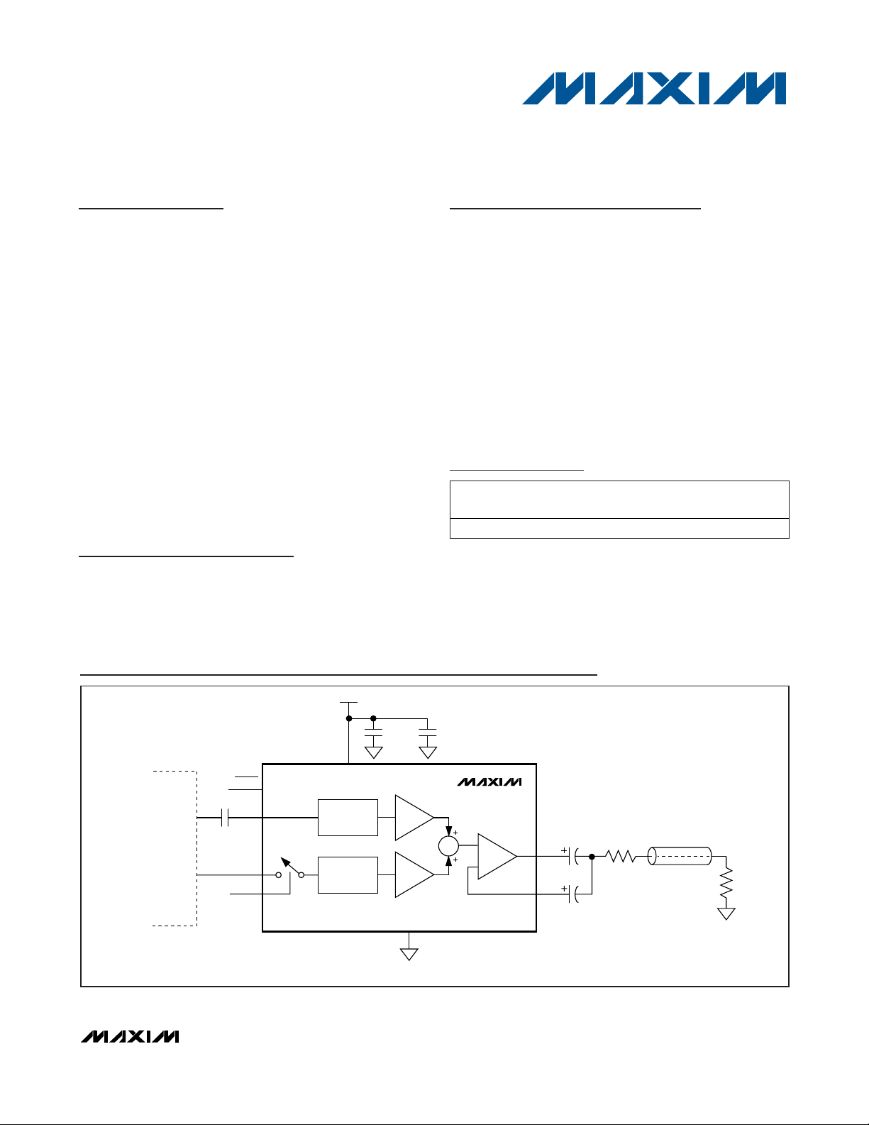
Functional Diagram
19-4031; Rev 0; 2/08
For pricing, delivery, and ordering information, please contact Maxim Direct at 1-888-629-4642,
or visit Maxim’s website at www.maxim-ic.com.
Pin Configuration appears at end of data sheet.
Ordering Information
+
Denotes lead-free package.
*
EP = Exposed pad.
µMAX is a registered trademark of Maxim Integrated Products, Inc.
PART TEMP RANGE
MAX11503EUA+ -40°C to +85°C 8 µMAX-EP* U8E+2
PINPACKAGE
PKG
CODE
V
CC
0.1µF
0.1µF*
PSAVE
YIN
CIN
CMUTE
TRANSPARENT
CLAMP
AC-COUPLING
AND BIAS
*REMOVE AND SHORT FOR DC-COUPLED OPERATION
BUFFER
BUFFER
SYSTEM
ON A
CHIP
Y
(SOC)
C
GND
1µF
Σ
MAX11503
+6dB
OUT
SAG
68µF*
33µF*
75Ω
75Ω
Page 2
MAX11503
Video Y/C Summer with
Driver and Chroma Mute
2 _______________________________________________________________________________________
ABSOLUTE MAXIMUM RATINGS
ELECTRICAL CHARACTERISTICS
(VCC= 3.0V, V
PSAVE
= VCC, V
CMUTE
= 0V, RL= 150Ω, AC-coupled, TA= +25°C, unless otherwise noted.)
Stresses beyond those listed under “Absolute Maximum Ratings” may cause permanent damage to the device. These are stress ratings only, and functional
operation of the device at these or any other conditions beyond those indicated in the operational sections of the specifications is not implied. Exposure to
absolute maximum rating conditions for extended periods may affect device reliability.
Any Pin to GND .....................................................-0.3V to +5.5V
Maximum Current into Any Pin Except V
CC
and GND....±-50mA
Continuous Power Dissipation (T
A
= +70°C)
8-Pin µMAX-EP
Single-Layer Board (derate 10.3mW/°C
above +70°C)...........................................................824mW
Multilayer Board (derate 12.9 mW/°C
above +70°C).........................................................1030mW
Operating Temperature Range ...........................-40°C to +85°C
Storage Temperature Range .............................-65°C to +150°C
Lead temperature (soldering, 10s) ..................................+300°C
Junction Temperature......................................................+150°C
ESD Protection (Human Body Model)..................................±2kV
PARAMETER SYMBOL CONDITIONS MIN TYP MAX UNITS
Operating Current I
Supply Voltage Range V
Operating Temperature
Range
Operating Current
(Power-Save Mode)
Maximum Output
Voltage
Frequency
Characteristic
Differential Phase dφ
Input AC-coupled to ground, no output load,
V
= 2.7V
CC
CC
CC
T -40 +85
I
CCS
V
OM
∆A
Input AC-coupled to ground, no output load,
V
= 3.0V
CC
Input AC-coupled to ground, no output load,
= 5.25V
V
CC
PSAVE = 0, VCC = 2.7V 0.5
PSAVE = 0, VCC = 3.0V 0.5
PSAVE = 0, VCC = 5.25V 0.5
VCC = 2.7V 2.0
VCC = 3.0V 2.2
VCC = 5.25V 2.4
VCC = 2.7V 6
VCC = 3.0V 6Voltage Gain A
V
VCC = 5.25V 6
YIN = 100kHz to 5.5MHz, VCC = 2.7V 0
YIN = 100kHz to 5.5MHz, VCC = 3.0V -1 0 +1
V
YIN = 100kHz to 5.5MHz, VCC = 5.25V 0
VCC = 2.7V 0.5
VCC = 3.0V 0.1Differential Gain dG
= 5.25V 0.12
V
CC
VCC = 2.7V 0.3
VCC = 3.0V 0.3
= 5.25V 0.3
V
CC
8
8 14.0
8
2.70 5.25 V
mA
o
C
µA
V
P-P
dB
dB
%
Degrees
Page 3
MAX11503
Video Y/C Summer with
Driver and Chroma Mute
_______________________________________________________________________________________ 3
ELECTRICAL CHARACTERISTICS (continued)
(VCC= 3.0V, V
PSAVE
= VCC, V
CMUTE
= 0V, RL= 150Ω, AC-coupled, TA= +25°C, unless otherwise noted.)
Typical Operating Characteristics
(VCC= 3.0V, V
PSAVE
= VCC, V
CMUTE
= 0V, RL= 150Ω, AC-coupled, TA= +25°C, unless otherwise noted.)
SUPPLY CURRENT
vs. SUPPLY VOLTAGE
MAX11503 toc01
SUPPLY VOLTAGE (V)
SUPPLY CURRENT (mA)
5.04.54.03.53.0
7
8
9
10
6
2.5 5.5
VIDEO OUTPUT WAVEFORM
(CMUTE = 0)
MAX11503 toc02
4µs/div
YIN
500mV/div
CIN
500mV/div
OUT
500mV/div
VIDEO OUTPUT WAVEFORM
(CMUTE = 1)
MAX11503 toc03
4µs/div
YIN
500mV/div
CIN
500mV/div
OUT
500mV/div
PARAMETER SYMBOL CONDITIONS MIN TYP MAX UNITS
Signal-to-Noise Ratio SNR
Second Harmonic
Distortion
Chroma Input
Resistance
Logic-Input Voltage
Low
Logic-Input Voltage
High
Weighted, VCC = 2.7V -65
Weighted, VCC = 3.0V -62
Weighted, V
= 5.25V -65
CC
3.58MHz, VCC = 2.7V -48
2HD
R
CIN
V
V
3.58MHz, VCC = 3.0V -48
3.58MHz, V
IL
IH
= 5.25V -48
CC
0.7 x
V
CC
800 kΩ
dB
dB
0.6 V
V
Page 4

MAX11503
Video Y/C Summer with
Driver and Chroma Mute
4 _______________________________________________________________________________________
Typical Operating Characteristics (continued)
(VCC= 3.0V, V
PSAVE
= VCC, V
CMUTE
= 0V, RL= 150Ω, AC-coupled, TA= +25°C, unless otherwise noted.)
20
0
-20
-40
RESPONSE (dB)
-60
-80
FREQUENCY RESPONSE
LUMA
CHROMA
0.1 1000
FREQUENCY (MHz)
100101
FIELD SQUARE WAVE
(AC-COUPLED OUTPUT)
MAX11503 toc06
VCC = 3V OR 5V
= 220µF
C
OUT
MAX11503 toc04
YIN
500mV/div
FIELD SQUARE WAVE
(DC-COUPLED OUTPUT)
4ms/div
FIELD SQUARE WAVE
(SAG-COUPLED OUTPUT)
VCC = 5V, C
C
SAG
= 33µF
OUT
MAX11503 toc05
MAX11503 toc07
= 68µF,
YIN
500mV/div
OUT
500mV/div
YIN
500mV/div
OUT
500mV/div
4ms/div
DIFFERENTIAL GAIN
0.2
0.1
0
DIFFERENTIAL GAIN (%)
-0.1
-0.2
17
MAX11503 toc08
DIFFERENTIAL PHASE (deg)
65432
0.4
0.3
0.2
0.1
0
-0.1
-0.2
-0.3
-0.4
17
4ms/div
DIFFERENTIAL PHASE
65432
OUT
500mV/div
MAX11503 toc09
Page 5

Detailed Description
The MAX11503 is a low-power video amplifier with a
Y/C summer and chroma mute. The device accepts an
S-video or Y/C input and sums the luma (Y) and chroma
(C) signals into a composite CVBS signal which can be
connected directly to a TV monitor. The MAX11503 drives
two terminated 75Ω video coax cables.
The MAX11503 features chroma mute, power save, and
SAG correction. Chroma mute disables the chroma
buffer. If the device is used to combine Y and C signals
in a camera application, chroma mute may be used in
low-light situations. This removes all chroma including
burst which causes a downstream composite video
decoder to interpret the video signal as luminance only,
thus improving image quality. Power-save puts the
device into a low-power consumption mode. SAG
correction allows small output capacitors to be used
in AC-coupled output applications.
The MAX11503 has a transparent clamp at YIN, allowing the luma input to be AC- or DC-coupled. If the luma
input is DC-coupled, the sync tip must be at ground
and the video signal must be 1V
P-P
. For low-supply
voltages, ensure that the DC level of the input is low
enough to avoid clipping at the output. If the luma input
is AC-coupled, the clamp adjusts the luma signal’s
sync tip to ground at YIN. Use an AC-coupling capacitor
of 0.1µF.
The MAX11503 has an internal AC-coupling capacitor
at CIN, allowing the chroma input to be coupled directly
to CIN.
Chroma Mute
In applications using cameras that output composite
video, the video is always decoded by a downstream
composite decoder in a monitor or for further video
processing.
In low-light conditions, the camera video signal
becomes noisy. The high-frequency (less visible monochrome) noise from the camera is transformed to lowfrequency highly visible colored noise by the normal
encode and decode blocks of composite video processing. This is caused when the chroma information is
encoded onto a high-frequency subcarrier, mixed with
the luminance and the decoded. First, high-frequency
noise near the color subcarrier is down-converted to
low-frequency noise. Second, chroma separation by
comb filtering removes luminance noise, but correlates
the noise in phase with the chroma to become vertical
lines. These two effects cause highly visible and objectional color noise. Hence, using a purely monochrome
signal is better looking than a color signal.
When pulled high, the chroma mute input disables all
chroma and burst and the device outputs a monochrome video signal. This causes the downstream
decoder to recognize the video signal as monochrome.
Power-Save
Asserting PSAVE logic low puts the device into a
power-down mode, reducing the supply current to
0.5µA and minimizing power consumption. Connect
PSAVE to VCCfor normal operation.
MAX11503
Video Y/C Summer with
Driver and Chroma Mute
_______________________________________________________________________________________ 5
Pin Description
PIN NAME FUNCTION
1 YIN Luma Input
2 GND Ground
3 OUT Video Out
4 SAG
5VCCPower Supply. Bypass to GND with 0.1µF and 1µF capacitors.
6 PSAVE
7 CMUTE
8 CIN Chroma Input
EP — Exposed Pad. Connect EP to ground.
Sag Correction Input. Connect to OUT when AC- or DC-coupling video output. See Figure 1 to determine
capacitor value and circuit.
Active-Low Power-Save Logic Input. Connect PSAVE to V
into a low-power consumption mode.
Chroma Mute Logic Input. Connect CMUTE to ground for normal operation. Drive high to disable the
chroma buffer.
for normal operation. Drive low to put device
CC
Page 6

MAX11503
Applications Information
Input Configuration
The luma input can be DC-coupled if the sync tip is near
ground (see the
Minimum Supply-Voltage Considerations
section). Otherwise, it should be AC-coupled into YIN
with a 0.1µF capacitor. When the luma input is AC-coupled, the transparent clamp adjusts its sync tip to
ground at YIN. Because the chroma input is internally
AC-coupled and biased, an external AC-coupling
capacitor is not required unless the signal is outside
the operating voltage range.
Output-Amplifier Configuration
The output buffer is capable of driving two terminated
AC- or DC-coupled 75Ω video coax cables. With sync
tip at the input at ground, the sync tip at the output is
offset by +250mV.
SAG-Corrected Output
SAG uses feedback to reduce the size of the output ACcoupling capacitor. Without SAG, a 220µF AC-coupling
capacitor is required to reduce tilt when feeding each
terminated 75Ω coax cable (Figure 2). This sets the
highpass -3dB frequency to 5Hz. Using SAG correction
with C
OUT
= 68µF and C
SAG
= 33µF also achieves a
highpass -3dB frequency of 5Hz, but with smaller
capacitors (Figure 1).
SAG correction is inherently designed to drive a constant load because the capacitor values vary with the
number of loads driven. If the capacitors are chosen for
two loads and the end user only connected one, the
video tilt would be opposite in sign, but of the same
magnitude as not using SAG at all. This would cause
excessive video tilt and the failure of the next piece of
equipment. The recommended capacitor values for two
constant 75Ω terminated video loads are C
OUT
=
120µF, C
SAG
= 68µF. In addition, SAG feedback predistortion function requires about 30% more overhead
in the video driver. Hence, use SAG correction only
with a typical 5V supply voltage. See the
Minimum
Supply-Voltage Considerations
section for calculations.
When SAG is not used, such as with AC- or DC-coupling
at the output, the driver can drive two terminated 75Ω
video coaxial cables. Connect SAG to OUT when not
using SAG correction.
Traditional AC-Coupled Output
The MAX11503 can also be configured to drive one or
two of the familiar terminated AC-coupled video coax
cables as shown in Figure 2.
Video Y/C Summer with
Driver and Chroma Mute
6 _______________________________________________________________________________________
Figure 1. Output with SAG Correction
Figure 2. Traditional AC-Coupled Output
MAX11503
C
OUT
68µF*
OUT
SAG
C
SAG
33µF*
*REMOVE AND SHORT FOR DC-COUPLED OPERATION
75Ω
75Ω
220µF*
75Ω
MAX11503
OUT
SAG
220µF*
75Ω
75Ω
*REMOVE AND SHORT FOR DC-COUPLED OPERATION
(a) (b)
MAX11503
OUT
SAG
75Ω
220µF*
75Ω
75Ω
Page 7

DC-Coupled Output
The MAX11503 input clamps the sync tip of the video
signal to 250mV at the IC output, forcing the blanking
level to be about 550mV on the coax cables at the termination resistor. This allows driving video to meet digital TV specifications without the need for costly
AC-coupling capacitors. Power dissipation is an especially important consideration if DC-coupling one or two
terminated video coax cables.
Minimum Supply-Voltage Considerations
The minimum supply voltage depends on the type of
video and the output configuration. Use at least the
minimum supply voltage to preserve the output amplifier’s linearity and video specifications.
The following examples discuss the required minimum
supply voltage under several scenarios. Unless otherwise specified, these examples assume:
1) The luma input is AC-coupled and therefore the
sync tip is clamped at 0.250V at the output.
2) The output amplifier needs 0.800V of overhead.
PAL
A PAL test signal is 1.235V
P-P
(100% color bars).
Therefore, the required minimum supply voltage is:
V
CC
= 2 x 1.235 + 0.250 + 0.800 = 3.5V
NTSC
A NTSC signal is 1.0V
P-P
(755 color bars). Therefore,
the required minimum supply voltage is:
VCC= 2 x 1.000 + 0.250 + 0.800 = 3.05V
Using SAG Correction
When using SAG correction, the output amplifier needs
an overhead of 800mV, in addition to 130% of the maximum video level at the output. Assuming an AC-coupled luma input:
For PAL, the minimum required supply voltage is:
VCC= 2 x 1.235 x 1.3 + 0.250 + 0.800 = 4.26V
For NTSC, the minimum required supply voltage is:
V
CC
= 2 x 1.000 x 1.3 + 0.250 +0.800 = 3.65V
Thermal Considerations
The power dissipation for single 75Ω terminated load is
64mW, and for two 75Ω terminated loads is 106mW. As
a result of the exposed pad, the temperature rise is
minimized.
Short-Circuit Protection
The MAX11503 outputs are fully protected against short
circuits either to the ground or the positive supply of the
device. The short-circuit protection circuitry limits the
output current to 130mA (typical) per output.
PCB Layout Recommendations
The MAX11503 has an exposed pad on the bottom.
The pad should be externally connected to ground.
Place power-supply decoupling capacitors close to the
device with short traces connecting to the power
planes. Use ceramic 0.1µF bypass and 1µF bulk
capacitors.
For a recommended PCB layout, refer to the MAX11503
EV kit data sheet.
MAX11503
Video Y/C Summer with
Driver and Chroma Mute
_______________________________________________________________________________________ 7
Pin Configuration
TOP VIEW
YIN
GND
OUT
SAG
*EXPOSED PAD
1
2
3
4
MAX11503
*
µMAX
8
7
6
5
CIN
CMUTE
PSAVE
V
CC
Page 8

MAX11503
Video Y/C Summer with
Driver and Chroma Mute
Maxim cannot assume responsibility for use of any circuitry other than circuitry entirely embodied in a Maxim product. No circuit patent licenses are
implied. Maxim reserves the right to change the circuitry and specifications without notice at any time.
8
_____________________Maxim Integrated Products, 120 San Gabriel Drive, Sunnyvale, CA 94086 408-737-7600
© 2008 Maxim Integrated Products is a registered trademark of Maxim Integrated Products, Inc.
Package Information
(The package drawing(s) in this data sheet may not reflect the most current specifications. For the latest package outline information,
go to www.maxim-ic.com/packages
.)
21-0107
8L, µMAX, EXP PAD.EPS
1
C
1
 Loading...