

General Description
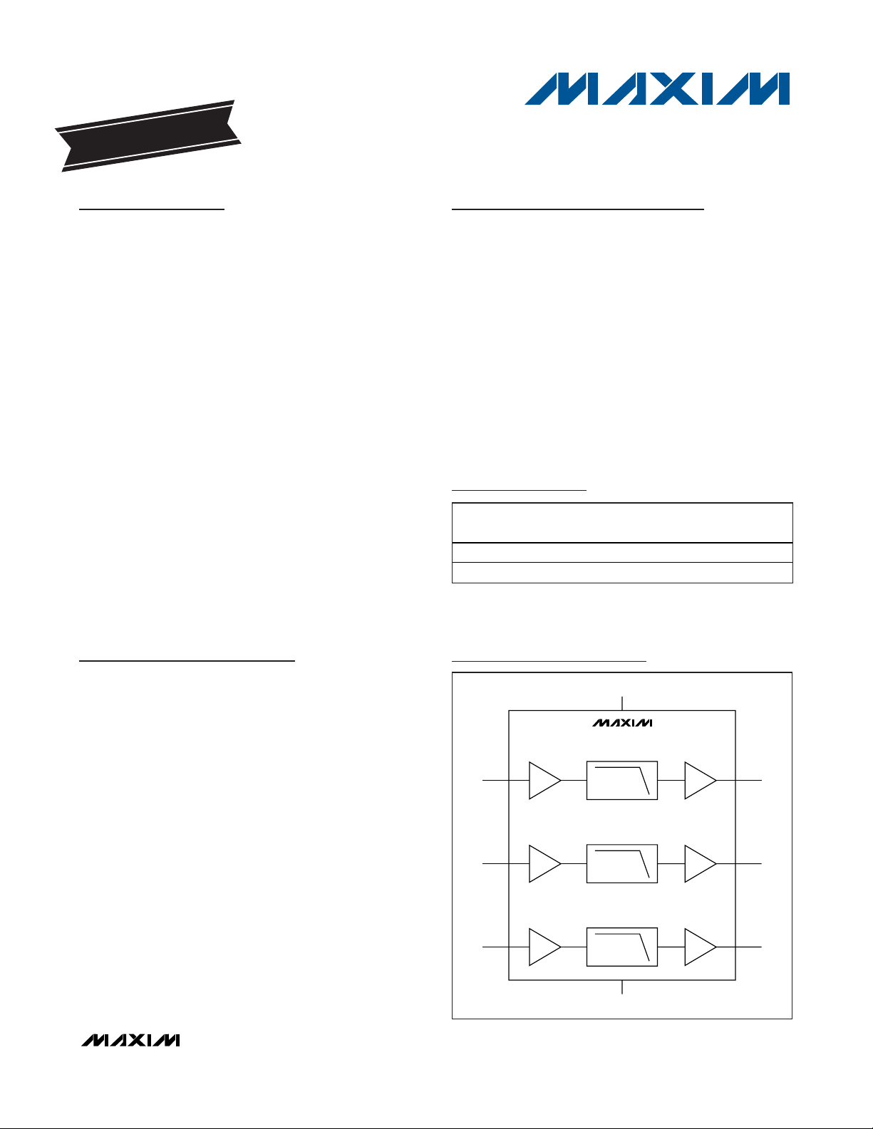
The MAX11501/MAX11502 integrated filters offer three
channels of 5th-order filters for standard-definition
video and include +6dB output buffers on each channel. These video filters are ideal for anti-aliasing and
DAC smoothing in applications such as set-top boxes,
security systems, digital video recorders (DVRs), DVD
players, and personal video recorders.
The MAX11501/MAX11502 video inputs feature a transparent clamp compatible with AC- and DC-coupled
input signals and allow DAC outputs to be directly coupled. The 5th-order filters provide a typical -3dB bandwidth of 8.6MHz (MAX11501) and 8.9MHz (MAX11502)
and offer either a flat passband response (MAX11501)
or a +0.8dB peaking passband response (MAX11502)
on all channels.
Each channel includes an output buffer with a gain of
+6dB capable of driving a full 2V
P-P
video signal into
two standard 150Ω (75Ω back-terminated) video loads.
The buffers drive either AC- or DC-coupled loads and
assure a blanking level of below 1V after the backmatch resistor.
The MAX11501/MAX11502 operate from a single +5V
supply and are available in the upper commercial 0°C
to +85°C temperature range. These devices are available in small 8-pin SO packages.
Applications
Set-Top Box Receivers
Digital Video Recorders (DVRs)
Security Video Systems
SDTV
DVD Players
Personal Video Recorders
Video On-Demand
Features
o Three-Channel 5th-Order 9MHz Filter for
Standard-Definition Video
o +6dB Output Buffers
o Transparent Input Clamp
o AC- or DC-Coupled Inputs
o AC- or DC-Coupled Outputs
o Flat Passband Response (MAX11501)
o +0.8dB Peaking Passband Response (MAX11502)
on All Channels
o 12kV HBM ESD Protection on Outputs
o Single +5V Power Supply
o Small 8-Pin SO Package
MAX11501/MAX11502
Three-Channel,
Standard-Definition Video Filters
________________________________________________________________
Maxim Integrated Products
1
19-3002; Rev 1; 4/08
For pricing, delivery, and ordering information, please contact Maxim Direct at 1-888-629-4642,
or visit Maxim’s website at www.maxim-ic.com.
EVALUATION KIT
AVAILABLE
Ordering Information
+
Denotes a lead-free package.
Note: All devices are specified over the 0°C to +85°C operating temperature range.
Typical Operating Circuit and Pin Configuration appear at end
of data sheet.
MAX11501
MAX11502
OUT1
+6dB
BUFFERTRANSPARENT
CLAMP
9MHz 5TH-ORDER
BUTTERWORTH
FILTER
IN1
OUT2
+6dB
IN2
OUT3
+6dB
IN3
V
CC
GND
Block Diagram
PART
MAX11501USA+ 8 SO Flat
MAX11502USA+ 8 SO HF Boost
PINPACKAGE
FREQUENCY
RESPONSE
MAX11501/MAX11502
Three-Channel,
Standard-Definition Video Filters
2 _______________________________________________________________________________________
ABSOLUTE MAXIMUM RATINGS
ELECTRICAL CHARACTERISTICS
(VCC= +5V, R
LOAD
= 150Ω to GND, CIN= 0.1µF, TA= 0°C to +85°C, frequency response is relative to 100kHz, unless otherwise noted.)
Stresses beyond those listed under “Absolute Maximum Ratings” may cause permanent damage to the device. These are stress ratings only, and functional
operation of the device at these or any other conditions beyond those indicated in the operational sections of the specifications is not implied. Exposure to
absolute maximum rating conditions for extended periods may affect device reliability.
VCCto GND..............................................................-0.3V to +6V
All other pins to GND ...-0.3V to the lower of (V
CC
+ 0.3V) and +6V
Continuous Power Dissipation (T
A
= +70°C)
8-Pin SO (derate 5.9mW/°C above +70°C)................. 470mW
Maximum Current into any Pin Except V
CC
and GND......±50mA
Operating Temperature Range
MAX1150_USA+ .................................................0°C to +85°C
Storage Temperature Range .............................-65°C to +150°C
Lead temperature (soldering, 10s) ..................................+300°C
Junction Temperature......................................................+150°C
)
PARAMETER SYMBOL CONDITIONS MIN TYP MAX UNITS
-1dB Bandwidth f
-3dB Bandwidth f
Stopband Attenuation A
Low-Frequency Gain A
Low-Frequency Gain Match A
Input Voltage Range V
Differential Gain dG All channels 0.1 %
Differential Phase dφ All channels 0.3 Degrees
Total Harmonic Distortion THD V
Channel-to-Channel Crosstalk X
Signal-to-Noise Ratio SNR NTC-7 weighting, 100kHz, 4.2MHz 80 dB
Propagation Delay t
Supply Voltage Range V
Supply Current I
Power-Supply Rejection Ratio PSRR DC (all channels) 60 dB
1dB
3dB
SB
V
V(MATCH
IN
TALK
PD
DD
CC
MAX11501 4.5 7.2
MAX11502 5 7.8
MAX11501 8.6
MAX11502 8.9
MAX11501, f = 27MHz 50
MAX11502, f = 27MHz 48
Referenced to GND if DC-coupled 1.4 V
= 1.8V
OUT
f = 1MHz -80 dB
f = 4.5MHz 76 ns
No load 18 26 mA
5.8 6.0 6.2 dB
0.02 dB
, f = 1MHz (all channels) 0.1 %
P-P
4.75 5 5.25 V
MHz
MHz
dB
MAX11501/MAX11502
Three-Channel,
Standard-Definition Video Filters
_______________________________________________________________________________________
3
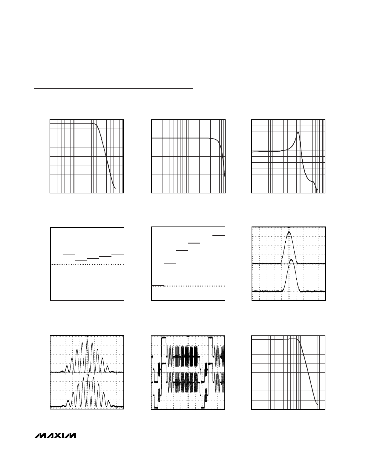
Typical Operating Characteristics
(VCC= 5V, RL= 150Ω to GND, output DC-coupled, TA= +25°C.)
MAX11501
FREQUENCY RESPONSE
10
0
-10
-20
-30
RESPONSE (dB)
-40
-50
-60
-70
0.1 100
FREQUENCY (MHz)
101
MAX11501 toc01
9
6
3
RESPONSE (dB)
0
-3
0.1 10
PASSBAND RESPONSE
MAX11501
DIFFERENTIAL GAIN, NTSC
0.2
0.1
0
DIFFERENTIAL GAIN (%)
-0.1
-0.2
17
STEP
65432
0.4
0.3
MAX11501 toc04
0.2
0.1
DIFFERENTIAL PHASE (deg)
-0.1
DIFFERENTIAL PHASE, NTSC
0
17
MAX11501
1
FREQUENCY (MHz)
MAX11501
STEP
120
100
MAX11501 toc02
80
60
DELAY (ns)
40
20
0
0.1 100
MAX11501 toc05
CH1
CH2
65432
CH1 = INPUT
CH2 = OUTPUT, AFTER BACKMATCH RESISTOR
MAX11501
GROUP DELAY
FREQUENCY (MHz)
MAX11501
2T RESPONSE
200ns/div
MAX11501 toc03
101
MAX11501 toc06
MODULATED 12.5T RESPONSE
MAX11501
CH1
CH2
CH1 = INPUT
CH2 = OUTPUT, AFTER BACKMATCH RESISTOR
400ns/div
MAX11501 toc07
MAX11501
MULTIBURST RESPONSE
CH1
CH2
CH1 = INPUT
CH2 = OUTPUT, AFTER BACKMATCH RESISTOR
10μs/div
MAX11501 toc08
MAX11502
FREQUENCY RESPONSE
10
0
-10
-20
-30
RESPONSE (dB)
-40
-50
-60
-70
0.1 100
FREQUENCY (MHz)
101
MAX11501 toc09
MAX11501/MAX11502
Three-Channel,
Standard-Definition Video Filters
4 _______________________________________________________________________________________
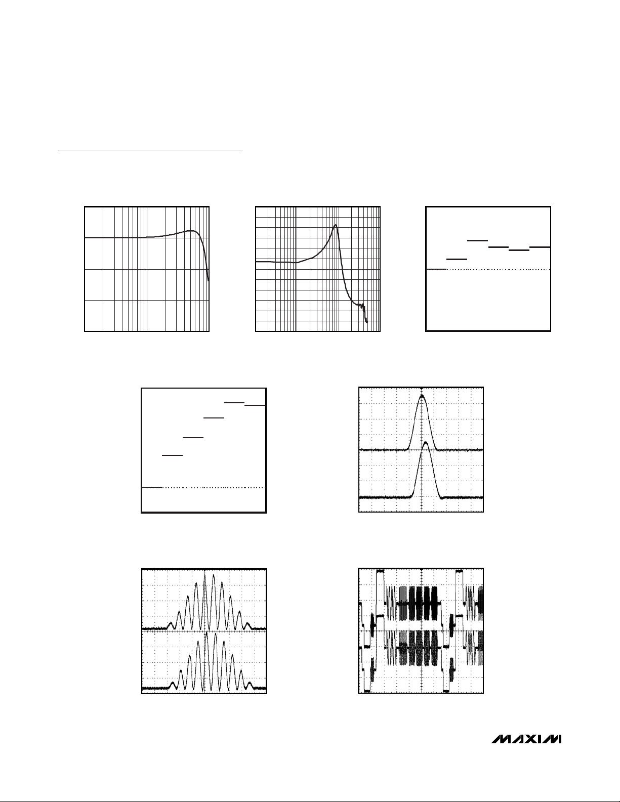
Typical Operating Characteristics (continued)
(VCC= 5V, RL= 150Ω to GND, output DC-coupled, TA= +25°C.)
MAX11502
PASSBAND RESPONSE
9
6
3
RESPONSE (dB)
0
-3
0.1 10
1
FREQUENCY (MHz)
MAX11501 toc10
120
100
80
60
DELAY (ns)
40
20
0
0.1 100
MAX11502
0.4
0.3
0.2
0.1
DIFFERENTIAL PHASE, NTSC
MAX11501 toc13
MAX11502
GROUP DELAY
FREQUENCY (MHz)
MAX11502
DIFFERENTIAL GAIN, NTSC
0.2
MAX11501 toc11
0.1
0
DIFFERENTIAL GAIN (%)
-0.1
-0.2
101
17
STEP
MAX11501 toc12
65432
MAX11502
2T RESPONSE
CH1
MAX11501 toc14
DIFFERENTIAL PHASE (deg)
0
-0.1
17
STEP
65432
MAX11502
MODULATED 12.5T RESPONSE
CH1
CH2
CH1 = INPUT
CH2 = OUTPUT, AFTER BACKMATCH RESISTOR
400ns/div
MAX11501 toc15
CH2
CH1 = INPUT
CH2 = OUTPUT, AFTER BACKMATCH RESISTOR
200ns/div
MAX11502
MULTIBURST RESPONSE
CH1
CH2
CH1 = INPUT
CH2 = OUTPUT, AFTER BACKMATCH RESISTOR
10μs/div
MAX11501 toc16

MAX11501/MAX11502
Three-Channel,
Standard-Definition Video Filters
_______________________________________________________________________________________ 5
Detailed Description
Each channel of the MAX11501/MAX11502 contains a
transparent input clamp, an 8.6MHz (MAX11501) or
8.9MHz (MAX11502), 5th-order lowpass filter and an
output amplifier with a gain of two (see the
Typical
Operating Circuit
). The MAX11501 provides a flat passband response and the MAX11502 features a +0.8dB
high-frequency boost at 5MHz on all channels to help
with system roll-off. Within the passband, each channel
amplifies the signal by two and adds 280mV of offset.
V
OUT
= (2 x VIN) + 0.28V
Typical voltage levels are shown in Figures 1 and 2.
Inputs
Transparent Clamps
All inputs feature transparent clamps to allow either AC
or DC input coupling. The clamp remains inactive while
the input signal is above ground, offering true DC input
coupling. If the signal goes below ground, as when the
signal is AC-coupled, the internal clamp sets the sync
tip at slightly below the ground level.
Figure 1. Typical AC-Coupled Signal
Pin Description
PIN NAME FUNCTION
1 IN1 Video Input Channel 1
2 IN2 Video Input Channel 2
3 IN3 Video Input Channel 3
4VCCPower Supply
5 GND Ground
6 OUT3 Video Output Channel 3
7 OUT2 Video Output Channel 2
8 OUT1 Video Output Channel 1
2.28V
1.0V
INPUT SIGNAL
0.3V
0.0V
OUTPUT SIGNAL
MAX11501
MAX11502
IN_ OUT_
0.88V
0.28V

MAX11501/MAX11502
Three-Channel,
Standard-Definition Video Filters
6 _______________________________________________________________________________________
Input Coupling
The choice of AC- or DC-coupling the input depends
on the video source. Many DACs provide a current output and are terminated to ground with a resistor. Such
DAC outputs are conveniently DC-coupled to the
MAX11501/MAX11502. Use AC-coupling when the DC
level of the video signal is unknown or outside the
specified input range of the MAX11501/MAX11502,
such as SCART or VCCterminated DAC outputs.
DC-Coupled Inputs
If the input is DC-coupled, the input voltage must
remain above zero but not exceed the maximum input
voltage of 1.4V (typical).
AC-Coupled Inputs
If the input is AC-coupled, the transparent clamps are
active and set the lowest point of the signal at ground.
This is appropriate for unipolar signals such as Y, R, G,
or B, with or without sync pulses (Figure 3).
For bipolar signals such as Pb and Pr, bias the AC-coupled inputs to a fixed DC voltage, typically 0.59V, to ensure
that the transparent clamp remains off. A suitable network
is shown in Figure 4. Determine the bias voltage using:
where ILis the input leakage current (typically 0.5µA).
Figure 2. Typical DC-Coupled Signal
Figure 3. Simple AC-Coupling for Unipolar Signals (Y, R, G, B)
Figure 4. AC-Coupling for Bipolar Signals (Pb, Pr)
2.32V
MAX11501
MAX11502
IN_ OUT_
1.02V
0.92V
INPUT SIGNAL
OUTPUT SIGNAL
0.32V
0.02V
0.00V
R
V
BCCL
2
=
+
RR
12
×−×
,
VIR
()
1
()
0.32V
R1
820kΩ
MAX11501
MAX11502
IN_
MAX11501
MAX11502
IN_
ENCODER
DAC
ENCODER
DAC
0.1μF
0.1μF
V
CC
R2
120kΩ

MAX11501/MAX11502
Three-Channel,
Standard-Definition Video Filters
_______________________________________________________________________________________ 7
Standard-Definition Filters
The MAX11501/MAX11502 filters are optimized to deliver
a flat (MAX11501) or high-frequency boosted (MAX11502)
passband and high stopband attenuation. The filter characteristics have been chosen to provide excellent time
domain response with low overshoot. The typical -3dB frequency of 8.6MHz (MAX11501) and 8.9MHz (MAX11502)
guarantee minimal attenuation in the passband while
at the same time offering a 27MHz attenuation of
typically -50dB (MAX11501) and -48dB (MAX11502).
Output Buffer
The MAX11501/MAX11502 feature output buffers with
+6dB of gain. A typical load (Figure 5(a)) is a 75Ω backmatch resistor, an optional 220µF or larger AC-coupling
capacitor, a transmission line, and a 75Ω termination
resistor. The MAX11501/MAX11502 clamp the signal,
forcing the blanking level to less than 1V at the termination resistor. This allows direct drive of video loads at
digital TV specifications without the need for costly ACcoupling capacitors. The MAX11501/MAX11502 drive
two parallel loads per output (Figure 5(b)), but thermal
considerations must be taken into account when doing
so (see the
Junction-Temperature Calculations
section).
Applications Information
Output Configuration
The MAX11501/MAX11502 outputs may be either DC- or
AC-coupled. When the outputs are AC-coupled, choose
a capacitor that passes the lowest frequency content of
the video signal, and keeps the line-time distortion within
desired limits. The capacitor value is a function of the
input leakage and impedance of the circuit being driven.
The MAX11501/MAX11502 easily drive the industry common 220µF, or larger, coupling capacitor. If any or all
outputs are driving two parallel loads, see the
Junction-
Temperature Calculations
section.
The MAX11501/MAX11502 outputs are fully protected
against short circuits to ground. The short-circuit protection circuitry limits the output current to 80mA (typical) per output. Shorting more than one output to
ground simultaneously may exceed the maximum
package power dissipation.
Junction-Temperature Calculations
Die temperature is a function of quiescent power dissipation and the power dissipation in the output drivers.
Calculate the power dissipated, PD, using:
PD= PDS+ P
DO1
+ P
DO2
+ P
DO3
where PDSis the quiescent power dissipated in the die,
and given by:
P
DS
= VCCx I
CC
and where P
DOn
is the power dissipated in the nth dri-
ver stage and given by:
where V
ORMSn
is the RMS output voltage and RLnis the
load resistance.
The following is an example of a junction-temperature
calculation, assuming the following conditions:
1) Video standard = 525/60/2:1.
2) Video format = RGB with syncs on all.
3) Picture content = 100% white.
4) The input signal is AC-coupled.
5) The output signal is DC-coupled.
6) VCC= 5.0V.
7) ICC= 26mA.
Figure 5. Typical Output Loads
VV V
()
CC ORMSn ORMSn
=
DOn
P
−
R
Ln
×
MAX11501
MAX11502
OUT_
220μF
(OPTIONAL)
Ω
75
Ω
75
(a) (b)
MAX11501
MAX11502
OUT_
75
75
Ω
Ω
220μF
(OPTIONAL)
220μF
(OPTIONAL)
75
75Ω
Ω

MAX11501/MAX11502
A sync tip exists at 280mV and peak white exists at
2.28V. The RMS voltage is approximately 1.88V on
each output (80% of the peak-to-peak voltage, plus the
offset) giving:
PDS= 5 x 0.026 = 0.13W
and
PD= 0.13 + 0.078 + 0.078 + 0.078 = 0.364W
The junction temperature is given by:
TJ= TA+ (R
θJA
x PD)
where TJis junction temperature, TAis ambient temperature (assume +70°C), and R
θJA
is thermal resistance
junction to ambient.
From the
Absolute Maximum Ratings
section of the data
sheet, the derating factor is 5.9mW/°C above +70°C.
R
θJA
= 1/(derating factor) = 1/(5.9mW/°C) = 170°C/W
(derating and maximum power dissipation are based on
minimum PCB copper and indicate worst case).
Therefore:
TJ= 70 + (170 x 0.364) = +132°C
In this example, the die temperature is below the
absolute maximum allowed temperature. It is unlikely
under normal circumstances that the maximum die
temperature will be reached, however it is possible if
tolerances of V
CC
, RL, input voltage etc. are consid-
ered and the ambient temperature is high.
Changing the above example to a single video load on
each output results in:
T
J
= +112°C
PCB Layout Recommendations
To help with heat dissipation, connect the power and
ground traces to large copper areas. Bypass VCCto
GND with 0.1µF and 1.0µF capacitors. Surface-mount
capacitors are recommended for their low inductance.
Place traces carrying video signals appropriately to
avoid mutual coupling. When AC-coupling the inputs,
place the capacitors as close as possible to the device
and keep traces short to minimize parasitic capacitance and inductance. For a recommended PCB layout, refer to the MAX11501/MAX11502 evaluation kit
datasheet.
Three-Channel,
Standard-Definition Video Filters
8 _______________________________________________________________________________________
75
×
=
.
0 078
. .
5 1 88 1 88
−
PW
DOn
()
=

MAX11501/MAX11502
Three-Channel,
Standard-Definition Video Filters
_______________________________________________________________________________________ 9
Typical Operating Circuit
OUT3
GNDV
CC
1
2
87OUT1
OUT2IN2
IN3
IN1
SO
+
TOP VIEW
3
4
6
5
MAX11501
MAX11502
Pin Configuration
+5V
V
CC
MAX11501
ENCODER
DAC
DAC
DAC
0.1μF* 220μF*
IN1
75Ω
0.1μF* 220μF*
75Ω
0.1μF* 220μF*
75Ω
TRANSPARENT
CLAMP
IN2
IN3
MAX11502
9MHz 5TH-ORDER
BUTTERWORTH
FILTER
GND
+6dB
BUFFER
+6dB
+6dB
75Ω
OUT1
75Ω
OUT2
75Ω
OUT3
*OPTIONAL CAPACITORS
75Ω
75Ω
75Ω

MAX11501/MAX11502
Three-Channel,
Standard-Definition Video Filters
10 ______________________________________________________________________________________
Package Information
For the latest package outline information, go to www.maxim-ic.com/packages.
PACKAGE TYPE PACKAGE CODE DOCUMENT NO.
8 SO S8+2
21-0041

MAX11501/MAX11502
Three-Channel,
Standard-Definition Video Filters
Maxim cannot assume responsibility for use of any circuitry other than circuitry entirely embodied in a Maxim product. No circuit patent licenses are
implied. Maxim reserves the right to change the circuitry and specifications without notice at any time.
Maxim Integrated Products, 120 San Gabriel Drive, Sunnyvale, CA 94086 408-737-7600 ____________________
11
© 2008 Maxim Integrated Products is a registered trademark of Maxim Integrated Products, Inc.
Heaney
Revision History
REVISION
NUMBER
0 12/07 Initial release —
1 4/08 Updated Block Diagram 1
REVISION
DATE
DESCRIPTION
PAGES
CHANGED
 Loading...