

General Description
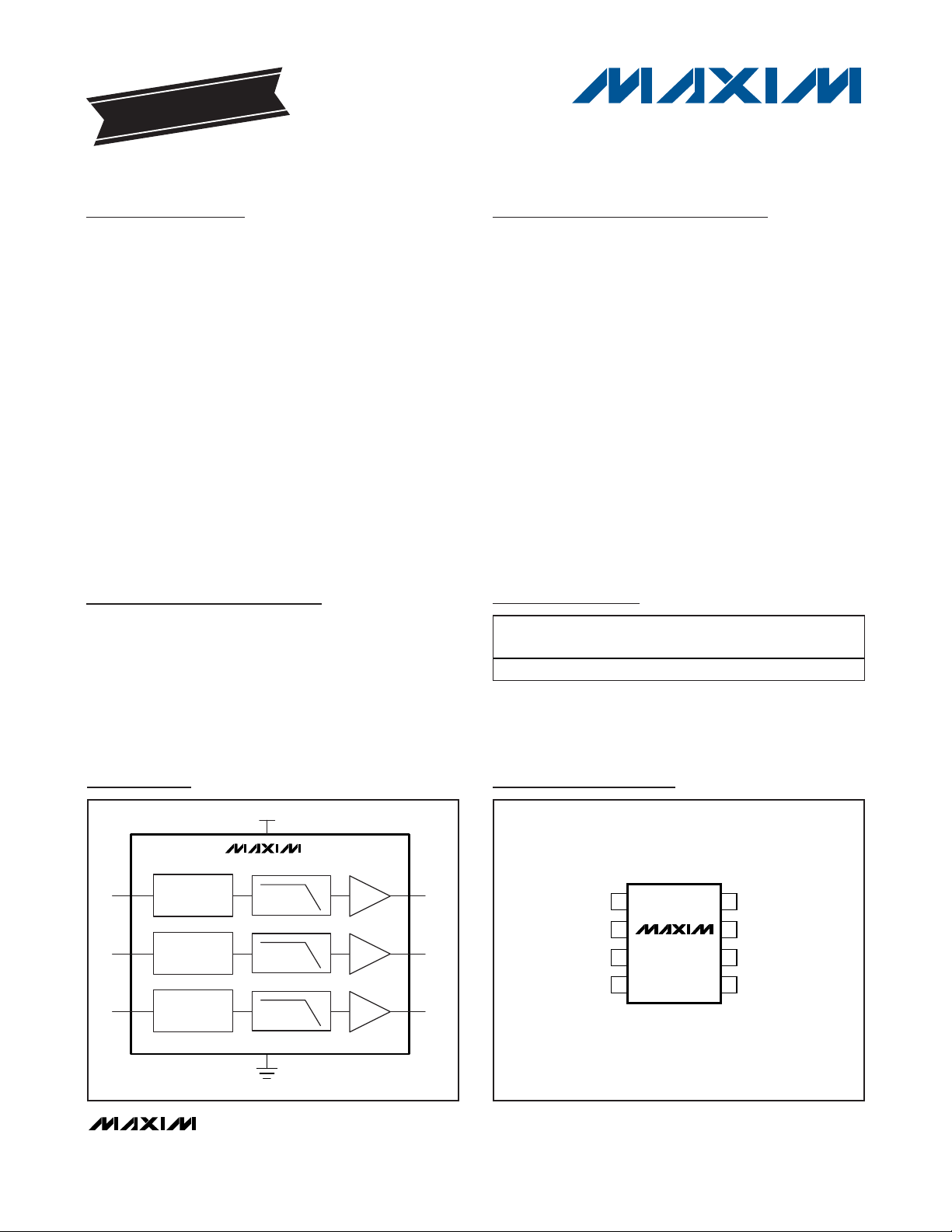
The MAX11500 integrated three-channel high-definition
(HD) video filter includes input video clamps and output
buffers. This device is ideal for anti-aliasing and DAC
smoothing video applications such as set-top boxes,
hard-disk recorders (HDRs), DVD players, and personal video recorders.
The 6th-order channel filters have a typical -3dB bandwidth of 33MHz. Each channel has an output buffer with
a gain of +6dB and can drive a full 2V
P-P
video signal
into one standard 150Ω video load. These buffers can
drive either an AC- or DC-coupled load such that the
blanking level voltage after the backmatch resistor is
less than 1V.
The video inputs feature a transparent clamp for ACand DC-coupled input signals. If the input signal does
not go below ground, the input clamp is inactive, thus
enabling DAC outputs to be DC-coupled to the input.
The device operates from a single +5V supply, is offered
in the upper commercial 0°C to +85°C temperature
range, and is available in a small 8-pin SO package.
Applications
High-Definition Set-Top Box Receivers
HD Television Sets
HD Recorders
DVD Players
Personal Video Recorders
Video-On-Demand
Features
♦ Three-Channel 6th-Order Filter for High-Definition
Video
♦ +6dB Output Buffers
♦ Transparent Input Clamps
♦ AC- or DC-Coupled Inputs
♦ AC- or DC-Coupled Outputs
♦ Output Buffers Drive One Standard 150Ω Video
Load
♦ 12kV HBM ESD Protection on Outputs
♦ Single +5V Power Supply
♦ Small 8-Pin SO package
MAX11500
Three-Channel, High-Definition Video Filter
________________________________________________________________
Maxim Integrated Products
1
OUT3
GNDV
CC
1
2
87OUT1
OUT2IN2
IN3
IN1
SO
+
TOP VIEW
3
4
6
5
MAX11500
Pin Configuration
IN1
OUT1
GND
V
CC
33MHz
TRANSPARENT
CLAMP
+6dB
IN2
OUT2
33MHz
TRANSPARENT
CLAMP
+6dB
IN3
OUT3
33MHz
TRANSPARENT
CLAMP
+6dB
MAX11500
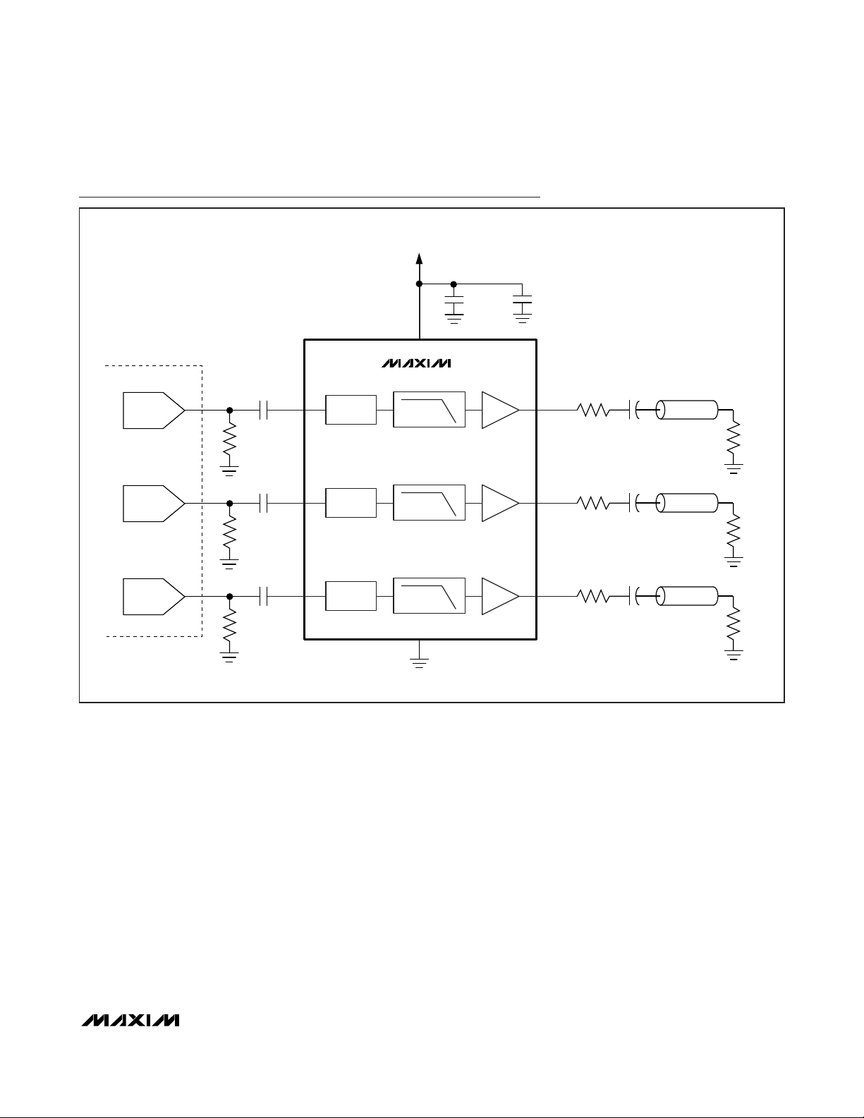
Typical Operating Circuit
19-3212; Rev 0; 1/08
For pricing, delivery, and ordering information, please contact Maxim Direct at 1-888-629-4642,
or visit Maxim’s website at www.maxim-ic.com.
Ordering Information
+
Denotes a lead-free package.
PART
PIN-
PKG
CODE
8 SO S8-2
EVALUATION KIT
AVAILABLE
TEMP RANGE
MAX11500USA+ 0°C to +85°C
PACKAGE
MAX11500
Three-Channel, High-Definition Video Filter
2 _______________________________________________________________________________________
ABSOLUTE MAXIMUM RATINGS
ELECTRICAL CHARACTERISTICS
(VCC= +5V, R
LOAD
= 150Ω to GND, CIN= 0.1µF, TA= 0°C to +85°C, unless otherwise specified. All frequency response is relative
to 100kHz.)
Stresses beyond those listed under “Absolute Maximum Ratings” may cause permanent damage to the device. These are stress ratings only, and functional
operation of the device at these or any other conditions beyond those indicated in the operational sections of the specifications is not implied. Exposure to
absolute maximum rating conditions for extended periods may affect device reliability.
Note 1: All devices are 100% production tested at TA= +25°C.
V
CC
to GND..............................................................-0.3V to +6V
All other pins to GND......-0.3V to the lower of (V
CC
+ 0.3V) and +6V
Continuous Power Dissipation (T
A
= +70°C)
8-Pin SO (derate 5.9mW/°C above +70°C)...............470.6mW
Maximum Current into any Pin Except V
CC
and GND......±50mA
Operating Temperature Range
MAX11500USA ...................................................0°C to +85°C
Storage Temperature Range .............................-65°C to +150°C
Lead Temperature (soldering, 10s) .................................+300°C
Junction Temperature......................................................+150°C
PARAMETER
CONDITIONS MIN TYP
UNITS
-1dB Bandwidth f
1dB
TA = +25°C 23 30 MHz
-3dB Bandwidth f
3dB
33 MHz
f = 37.125MHz 6.5
f = 44.25MHz 15.5
Stopband Attenuation A
SB
f = 74.25MHz, TA = +25°C 32 48
dB
Low-Frequency Gain A
V
5.4 6.0 6.6 dB
Low-Frequency Gain
Matching
)
0.01 dB
Input Voltage Range V
IN
Referenced to GND if DC-coupled 1.7 V
V
OUT
= 1.4V
P-P
, f = 10MHz 0.15
V
OUT
= 1.4V
P-P
, f = 15MHz 0.2
Total Harmonic
Distortion
THD
V
OUT
= 1.4V
P-P
, f = 22MHz 0.8
%
Channel-to-Channel
Crosstalk
X
TALK
f = 1MHz -72 dB
Signal-to-Noise Ratio SNR
Peak signal (2V
P-P
) to RMS noise,
f = 100kHz to 30MHz
68 dB
Group Delay t
g
f = 100kHz 25 ns
∆t
g
f = 100kHz to 26MHz 8 ns
V
CC
4.75 5 5.25 V
Supply Current I
CC
No load 24 38 mA
SYMBOL
MAX
Group-Delay Deviation
Supply Voltage Range
A
V(MATCH
MAX11500
Three-Channel, High-Definition Video Filter
_______________________________________________________________________________________
3
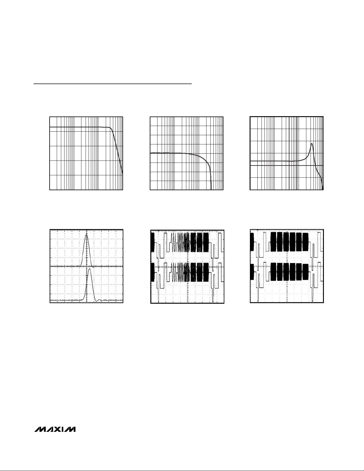
MAGNITUDE RESPONSE
(PASSBAND AND STOPBAND)
MAX11500 toc01
FREQUENCY (MHz)
RESPONSE (dB)
101
-60
-40
-20
0
20
-80
0.1 100
MAGNITUDE RESPONSE
(PASSBAND)
MAX11500 toc02
FREQUENCY (MHz)
RESPONSE (dB)
101
4.5
5.0
5.5
6.0
6.5
7.0
7.5
8.0
4.0
0.1 100
GROUP DELAY
MAX11500 toc03
FREQUENCY (MHz)
DELAY (ns)
101
10
20
30
40
50
60
0
0.1 100
2T RESPONSE
MAX11500 toc04
40ns/div
200mV/div
200mV/div
HD MULTIBURST RESPONSE
(1MHz–10MHz)
MAX11500 toc05
4µs/div
200mV/div
200mV/div
HD MULTIBURST RESPONSE
(20MHz–30MHz)
MAX11500 toc06
4µs/div
200mV/div
200mV/div
Typical Operating Characteristics
(VCC= +5V, outputs AC-coupled with 220µF, R
LOAD
= 150Ω to GND, CIN= 0.1µF, TA= +25°C. All frequency response is relative to
100kHz.)
Detailed Description
The MAX11500 integrates three high-definition (HD)
video filters, each with a transparent input clamp, a 6thorder lowpass filter with a -3dB bandwidth of 33MHz,
and an output stage with a gain of 2V/V. The output signal is offset by typically 550mV to optimize driver performance.
V
OUT
= 2 x VIN+ 0.55V
Typical voltage waveforms are shown in Figures 1 and 2.
Transparent Clamps
All inputs feature a transparent clamp that allows either
AC- or DC-coupling of the inputs. The clamp remains
inactive while the input signal is above ground, offering
true DC input coupling. If the signal goes below
ground, as is the case if it is AC-coupled, the clamp
sets the sync tip close to the ground level.
Input Coupling
The choice to AC- or DC-couple the input depends on
the video source. Many DACs have a current output
and are terminated to ground with a resistor; such signals can be conveniently DC-coupled. In cases where
the DC level of the video signal is unknown or outside
of the specified input range of the MAX11500, such signals require AC-coupling. Examples of the latter are
SCART inputs and DACs terminated to VCC.
DC-Coupled Inputs
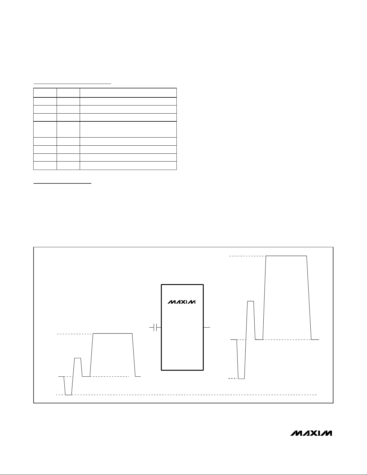
If the input is DC-coupled, the voltage must remain
above zero but not exceed the maximum input voltage
of 1.7V (typical).
INPUT SIGNAL
0.3V
1.0V
0.0V
OUTPUT SIGNAL
1.15V
2.55V
0.55V
IN_ OUT_
MAX11500
Figure 1. Typical AC-Coupled Signal
MAX11500
Three-Channel, High-Definition Video Filter
4 _______________________________________________________________________________________4 _______________________________________________________________________________________
Pin Description
PIN
FUNCTION
1 IN1 Video Input Channel 1
2 IN2 Video Input Channel 2
3 IN3 Video Input Channel 3
4V
CC
Power Supply. Bypass to GND with 0.1µF
and 1µF capacitors.
5
Ground
6
Video Output Channel 3
7
Video Output Channel 2
8
Video Output Channel 1
NAME
GND
OUT3
OUT2
OUT1
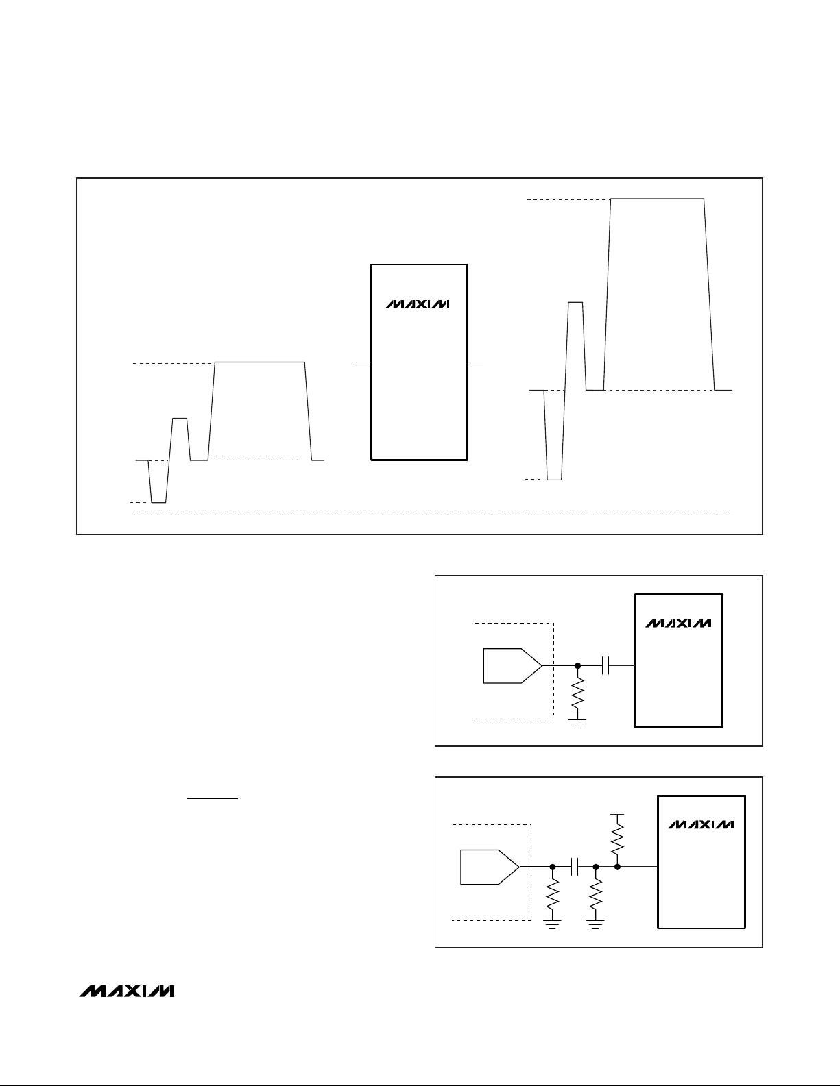
AC-Coupled Inputs
If the input is AC-coupled, the transparent clamp will be
active and sets the sync tip or the lowest voltage of the
signal close to ground. This clamping behavior is
appropriate for unipolar signals such as Y, R, G, or B
with or without sync pulse (Figure 3).
For bipolar signals such as Pb, Pr signals, the AC-coupled
inputs should be biased to a fixed DC voltage to ensure
that the transparent clamp never turns on. A suitable
network that biases the input to typically 0.59V is shown
in Figure 4. The device has an input leakage current
(IL) of typically 0.5µA and thus the bias voltage is
derived as follows:
HD Filters
The internal filters are optimized to deliver a flat passband along with high stopband attenuation. The filter
characteristic has been chosen to provide an excellent
time-domain response with low overshoot. The typical
-3dB frequency of 33MHz guarantees low attenuation
in the passband, while at the same time allowing for a
typical attenuation of -48dB at 74.25MHz.
V
R
RR
VIxR
BCCL
( )=
+
−
2
12
1
MAX11500
Three-Channel, High-Definition Video Filter
_______________________________________________________________________________________ 5
INPUT SIGNAL
0.32V
1.02V
0.02V
0.00V
OUTPUT SIGNAL
1.19V
2.59V
0.59V
IN_ OUT_
MAX11500
Figure 2. Typical DC-Coupled Signal
IN_
MAX11500
0.1µF
ENCODER
DAC
Figure 3. AC-Coupling for Unipolar Signals (Y, R, G, B)
IN_
R1
820kΩ
R2
120kΩ
MAX11500
0.1µF
ENCODER
DAC
V
CC
Figure 4. AC-Coupling for Bipolar Signals (Pb, Pr)

MAX11500
Three-Channel, High-Definition Video Filter
6 _______________________________________________________________________________________
Output Buffer
The MAX11500 features output buffers with +6dB gain
that drive a standard 150Ω video load. A typical load
consists of a 75Ω backmatch resistor, an optional
220µF or larger coupling capacitor, and a 75Ω termina-
tion resistor. The offset between input and output signals has been chosen such that the blanking level on
the output is less than 1V after the backmatch resistor,
thus meeting digital TV specifications. This allows the
MAX11500 to drive video loads directly without using
costly AC-coupling capacitors.
Applications Information
Output Considerations
The MAX11500 outputs can be DC- or AC-coupled.
The MAX11500, with +6dB gain, is typically connected
to a 75Ω series backmatch resistor followed by the
video cable. If an AC connection is used, choose an
AC-coupling capacitor value that ensures that the lowest frequency content in the video signal is passed and
the field-time distortion is kept within desired limits. The
selection of this value is a function of the input impedance and more importantly the input leakage of the circuit being driven. Common industry practice is to use a
220µF or larger capacitor.
The outputs of the MAX11500 are fully protected
against a short circuit either to the ground or the positive supply of the device. The short-circuit protection
circuitry limits the output current to typically 75mA per
output. Shorting more than one output simultaneously
may exceed the maximum package power dissipation.
PCB Layout Recommendations
The device is thermally designed to operate with minimum copper. However, to help with heat dissipation,
connect the power and ground traces to large copper
areas if possible. Bypass VCCto GND with a 0.1µF
capacitor and an additional 1µF capacitor in parallel for
additional low-frequency decoupling. Using surfacemount capacitors reduces lead inductance and
ensures that the impedance of the capacitors is low
over a broad range of frequencies.
Place traces carrying video signals appropriately to
avoid mutual coupling. If AC-coupling the inputs, place
the input coupling capacitors as close as possible to
the device and keep traces short to minimize parasitic
capacitance and inductance. Doing so extends the
performance to the uppermost frequency range possible with the MAX11500.
For a recommended PCB layout, refer to the MAX11500
EV kit data sheet.
MAX11500
Three-Channel, High-Definition Video Filter
_______________________________________________________________________________________ 7
IN1
0.1µF*
0.1µF1µF
220µF*
1
75Ω
75Ω
75Ω
OUT1
GND
*OPTIONAL
V
CC
33MHz
CLAMP
ENCODER
+6dB
8
MAX11500
DAC
IN2
0.1µF* 220µF*
2
75Ω
75Ω
75Ω
OUT2
33MHz
CLAMP
+6dB
7
DAC
IN3
0.1µF* 220µF*
3
75Ω
75Ω
75Ω
OUT3
33MHz
CLAMP
5
4
+5V
+6dB
6
DAC
Typical Operating Circuit

MAX11500
Three-Channel, High-Definition Video Filter
Maxim cannot assume responsibility for use of any circuitry other than circuitry entirely embodied in a Maxim product. No circuit patent licenses are
implied. Maxim reserves the right to change the circuitry and specifications without notice at any time.
8
_____________________Maxim Integrated Products, 120 San Gabriel Drive, Sunnyvale, CA 94086 408-737-7600
© 2008 Maxim Integrated Products is a registered trademark of Maxim Integrated Products, Inc.
Package Information
(The package drawing(s) in this data sheet may not reflect the most current specifications. For the latest package outline information,
go to www.maxim-ic.com/packages
.)
N
1
TOP VIEW
D
e
FRONT VIEW
INCHES
DIM
MIN
0.053A
0.004
A1
0.014
B
0.007
C
e 0.050 BSC 1.27 BSC
0.150
HE
A
B
A1
C
L
E
H 0.2440.228 5.80 6.20
0.016L
VARIATIONS:
INCHES
MINDIM
D
0.189 0.197 AA5.004.80 8
0.337 0.344 AB8.758.55 14
D
0\-8\
MAX
0.069
0.010
0.019
0.010
0.157
0.050
MAX
0.3940.386D
MILLIMETERS
MAX
MIN
1.35
1.75
0.10
0.25
0.35
0.49
0.19
0.25
3.80 4.00
0.40 1.27
MILLIMETERS
MAX
MIN
9.80 10.00
N MS012
16
AC
SOICN .EPS
SIDE VIEW
PROPRIETARY INFORMATION
TITLE:
PACKAGE OUTLINE, .150" SOIC
APPROVAL
21-0041
REV.DOCUMENT CONTROL NO.
1
B
1
 Loading...