

19-1100; Rev 0; 6/96
EVALUATION KIT
AVAILABLE
8-Bit, 300Msps Flash ADC
_______________General Description
The MAX1125 is a monolithic, flash analog-to-digital converter (ADC) capable of digitizing a 2V analog input signal
into 8-bit digital words at a typical 300Msps update rate.
For most applications, no external sample-and-hold is
required for accurate conversion due to the device's
narrow aperture time, wide bandwidth, and low input
capacitance. A single standard -5.2V power supply is
required to operate the MAX1125, with nominal 2.2W
power dissipation. A special decoding scheme reduces
metastable errors to 1LSB.
The part is packaged in a 42-pin ceramic sidebraze
that is pin compatible with the CX20116 and
CX41396D. The surface-mount 44-pin CERQUAD package allows access to additional reference ladder taps,
an overrange bit, and a data-ready output. The pincompatible 150Msps MAX1114 is also available.
________________________Applications
Digital Oscilloscopes
Transient Capture
Radar, EW, ECM
Direct RF Down-Conversion
Medical Electronics
Ultrasound, CAT Instrumentation
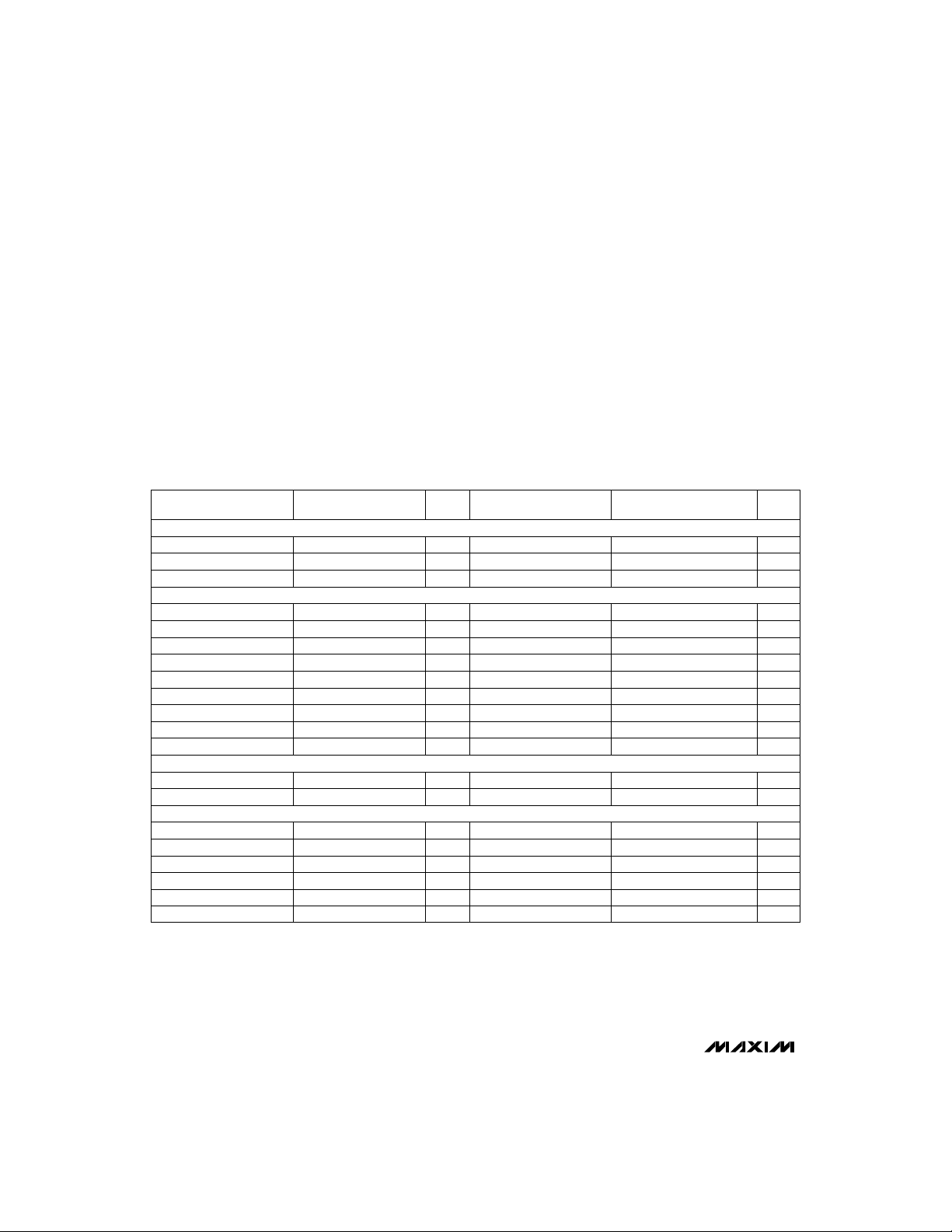
_________________Pin Configurations
TOP VIEW
DGND
AGND
V
EE
MINV
CLK
CLK
V
EE
AGND
AGND
VRBS
VRBF
D7D6D5D4D3D2D1
D8 (MSB)
42
41
43
44
1
2
3
4
5
6
7
8
9
10
11
12
EE
V
40
MAX1125
13
14
15
16
VIN
VR1
AGND
AGND
CERQUAD
D0 (LSB)
DREADY
39
38
18
17
VR2
AGND
DGND
36
35
37
34
33
AGND
32
V
EE
31
LINV
30
N.C.
29
DRINV
28
N.C.
V
27
EE
26
AGND
25
AGND
24
VRTS
23
VRTF
22
21
20
19
EE
V
VIN
VR3
AGND
____________________________Features
♦ Metastable Errors Reduced to 1LSB
♦ 10pF Input Capacitance
♦ 210MHz Input Bandwidth
♦ 300Msps Conversion Rate
♦ 2.2W Typical Power Dissipation
♦ Single -5.2V Supply
______________Ordering Information
PART
MAX1125AIDO
MAX1125BIDO
MAX1125AIBH -20°C to +85°C
MAX1125BIBH -20°C to +85°C 44 CERQUAD ±1
Functional Diagram appears at end of data sheet.
TEMP. RANGE PIN-PACKAGE
-20°C to +85°C
-20°C to +85°C
42 Ceramic SB
42 Ceramic SB
44 CERQUAD
INL (LSBs)
±0.75
±1
±0.75
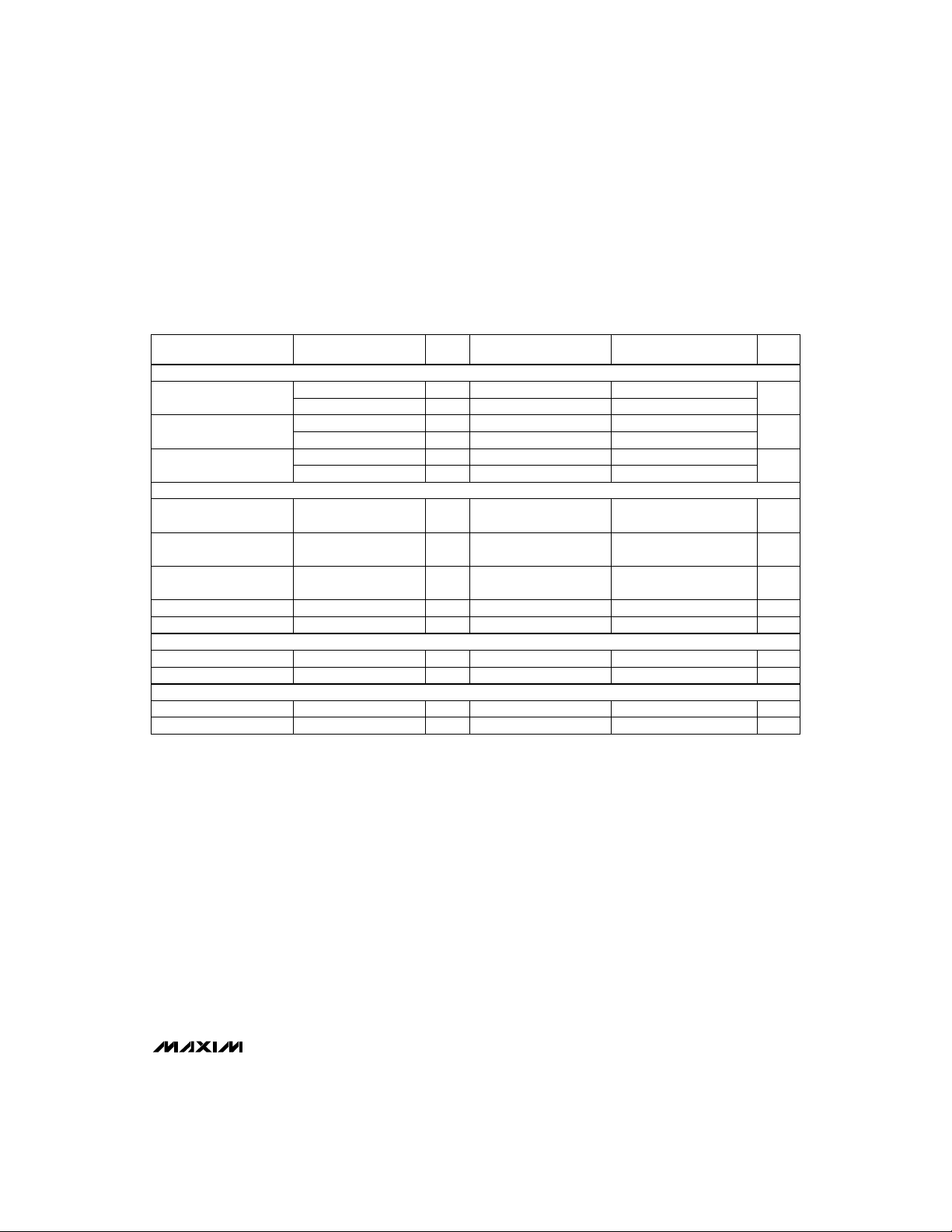
____Pin Configurations (continued)
TOP VIEW
N.C.
42
VRTF
41
N.C.
40
V
EE
39
V
EE
38
N.C.
37
N.C.
36
AGND
35
VIN
34
AGND
33
VR2
32
AGND
31
VIN
30
AGND
29
N.C.
28
N.C.
27
V
26
EE
V
25
EE
N.C.
24
VRBF
23
N.C.
22
N.C.
LINV
AGND
DGND
DO (LSB)
D7 (MSB)
DGND
AGND
MINV
N.C.
CLK
CLK
V
1
EE
2
3
V
4
EE
5
6
7
8
D1
9
D2
10
D3
11
D4
12
D5
13
D6
14
15
16
17
V
EE
18
19
20
21
MAX1125
Ceramic SB
MAX1125
________________________________________________________________
Maxim Integrated Products
1
For free samples & the latest literature: http://www.maxim-ic.com, or phone 1-800-998-8800
8-Bit, 300Msps Flash ADC
ABSOLUTE MAXIMUM RATINGS
Negative Supply Voltage (VEETO GND) ..............-7.0V to +0.5V
Ground Voltage Differential...................................-0.5V to +0.5V
Analog Input Voltage...............................................V
Reference Input Voltage..........................................V
Digital Input Voltage ................................................V
Reference Current V
Stresses beyond those listed under “Absolute Maximum Ratings” may cause permanent damage to the device. These are stress ratings only, and functional
operation of the device at these or any other conditions beyond those indicated in the operational sections of the specifications is not implied. Exposure to
MAX1125
absolute maximum rating conditions for extended periods may affect device reliability.
RTF
to V
........................................25mA
RBF
to +0.5V
EE
to +0.5V
EE
to +0.5V
EE
ELECTRICAL CHARACTERISTICS
(VEE= -5.2V, R
unless otherwise noted.)
DC ACCURACY
ANALOG INPUT
REFERENCE INPUT
TIMING CHARACTERISTICS
CLK-to-Data Ready Delay
= 50Ω, VRBF = -2.00V, VR2 = -1.00V, VRTF = 0.00V, f
SOURCE
CONDITIONSPARAMETER
RT
RB
(tD)
TEST
LEVEL
Digital Output Current ...........................................0mA to -30mA
Operating Temperature Range ...........................-25°C to +85°C
Junction Temperature......................................................+150°C
Storage Temperature Range.............................-65°C to +150°C
Lead Temperature (soldering, 10sec).............................+300°C
= 150MHz, 50% Duty Cycle, TA= T
CLK
MAX1125A
MIN TYP MAX
VI
VI
GuaranteedNo Missing Codes
IV
IV
VI
V
V
VI
V
V
V
VI
V
VI
V
V
V
V
V
MAX1125B
MIN TYP MAX
-0.95 ±0.80 +0.95
-0.95 +0.95
Guaranteed
-30 +30
-30 +30
-2.0 0.0
10
15
250 500
1,000
210
335
100 200 300
10
250 300
2.4
2
2.0
5
1.5
MIN
to T
MAX
UNITS
LSB-0.75 ±0.60 +0.75Integral Linearity
LSB-0.75 +0.75Differential Linearity
mV-30 +30Offset Error V
mV-30 +30Offset Error V
V-2.0 0.0Input Voltage Range
pF10Over full input rangeInput Capacitance
kΩ15Input Resistance
µA250 500Input Current
V/µs1,000Input Slew Rate
MHz210VIN = full scaleLarge Signal Bandwidth
MHz335IN = 500mVp-pSmall Signal Bandwidth
Ω100 200 300Ladder Resistance
MHz10Reference Bandwidth
Msps250 300Maximum Sample Rate
ns2.4Clock to Data Delay
ps/°C2Output Delay TEMPCO
ns2.0
ps5Aperture Jitter
ns1.5Acquisition Time
,
2 _______________________________________________________________________________________
8-Bit, 300Msps Flash ADC
ELECTRICAL CHARACTERISTICS (continued)
(VEE= -5.2V, R
unless otherwise noted.)
DYNAMIC PERFORMANCE
Signal-to-Noise Ratio
Total Harmonic Distortion
Signal-to-Noise and
Distortion (SINAD)
DIGITAL INPUTS
Digital Input High Voltage
(MINV, LINV)
Digital Input Low Voltage
(MINV, LINV)
Clock Synchronous
Input Currents
DIGITAL OUTPUTS
POWER-SUPPLY REQUIREMENTS
TEST LEVEL CODES
All electrical characteristics are subject to the
following conditions:
All parameters having min/max specifications are
guaranteed. The Test Level column indicates the
specific device testing actually performed during
production and Quality Assurance inspection.
Any blank section in the data column indicates
that the specification is not tested at the specified
condition.
Unless otherwise noted, all tests are pulsed;
therefore, Tj= TC= TA.
= 50Ω, VRBF = -2.00V, VR2 = -1.00V, VRTF = 0.00V, f
SOURCE
CONDITIONSPARAMETER
FIN= 100MHz
PWL
PWH
TEST
LEVEL
TEST LEVEL
I
II
III
IV
V
VI
VI
VI
VI
VI
VI
VI
VI
VI
V
VI
VI
VI
VI
V
I
I
TEST PROCEDURE
100% production tested at the specified temperature.
100% production tested at T
specified temperatures.
QA sample tested only at the specified temperatures.
Parameter is guaranteed (but not tested) by design and
characterization data.
Parameter is a typical value for information purposes only.
100% production tested at T
over specified temperature range.
= 150MHz, 50% Duty Cycle, TA= T
CLK
MAX1114A
MIN TYP MAX
45 47FIN= 3.58MHz
39 42
-48 -52FIN= 3.58MHz
-40 -43FIN= 100MHz
44 46FIN= 3.58MHz
37 39FIN= 100MHz
to T
MIN
MAX1114B
MIN TYP MAX
44 46
38 41
-46 -50
-39 -42
42 44
35 37
-1.1 -0.7
-2.0 -1.5
40
2 1.8
2 1.8
-1.1
-1.5
2.4
425 550
2.2 2.9
= +25°C, and sample tested at the
A
= +25°C. Parameter is guaranteed
A
MAX
UNITS
dB
dB
dB
V-1.1 -0.7
V-2.0 -1.5
µA40
ns2 1.8Clock Low Width, T
ns2 1.8Clock High Width, T
V-1.150Ωto -2VDigital Output High Voltage
V-1.550Ω to -2VDigital Output Low Voltage
ns2.4
mA425 550TA= +25 °CSupply Current
W2.2 2.9TA= +25 °CPower Dissipation
MAX1125
,
_______________________________________________________________________________________
3
8-Bit, 300Msps Flash ADC
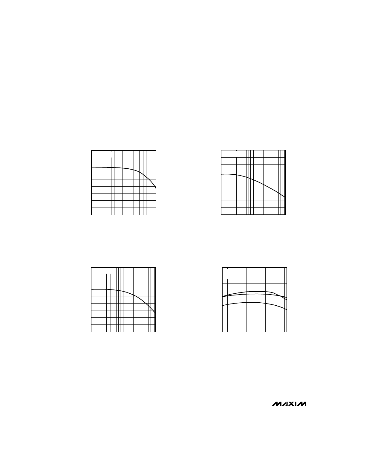
__________________________________________Typical Operating Characteristics
52
MAX1125
fs = 250Msps
50
48
46
44
42
SNR (dB)
40
38
36
34
1 10 100
SIGNAL-TO-NOISE AND DISTORTION
52
fs
50
48
46
44
42
SINAD (dB)
40
38
36
34
1 10 100
SIGNAL-TO-NOISE RATIO
vs. INPUT FREQUENCY
INPUT FREQUENCY (MHz)
vs. INPUT FREQUENCY
= 250Msps
INPUT FREQUENCY (MHz)
TOTAL HARMONIC DISTORTION
vs. INPUT FREQUENCY
75
fs = 250Msps
MAX1125 -01
70
65
60
55
50
THD (dB)
45
40
35
30
1 10 100
INPUT FREQUENCY (MHz)
MAX1125 -02
SNR, THD, SINAD
vs. TEMPERATURE
50
fs
MAX1125 -03
SNR, THD, SINAD (dB)
= 250Msps
= 100MHz
f
IN
45
40
SINAD
35
30
-40 -20
80
SNR
0
20 40
TEMPERATURE (°C)
THD
MAX1125 -04
60
4 _______________________________________________________________________________________

8-Bit, 300Msps Flash ADC
______________________________________________________________Pin Description
PIN
Ceramic SB
1, 4, 17, 25, 26, 38, 39 Negative Analog Supply (nominally -5.2V)
2, 19, 22, 24, 27, 28, 36,
37, 40, 42
3 D0–D6 Output Inversion Control LINV31
5, 16, 29, 31, 33, 35 Analog GroundAGND
6, 15 Digital Ground
7 Digital Data Output (LSB)
8–13 Digital Data Output
14 Digital Data Output (MSB)
18 D7 Output Inversion ControlMINV4
— Overrange Output
20
21
—
23 Reference Voltage Bottom, ForceVRBF11
30, 34
— Reference Voltage Tap 1 (typically -1.5V)VR113
32 Reference Voltage Tap 2 (typically -1V)
— Reference Voltage Tap 3 (typically -0.5V)VR321
41 Reference Voltage Top, Force
— Reference Voltage Top, Sense
—
— Data-Ready Output
CERQUAD
3, 7, 12, 22, 27, 32
28, 30
2, 8, 9, 14, 16, 18, 20,
25, 26, 33
1, 34
36
37–42
43
44
5
6
10
15, 19
17
23
24
29
35
NAME
V
EE
N.C.
DGND
D0
D1–D6
D7
D8
CLK
CLK
VRBS
VIN
VR2
VRTF
VRTS
DRINV
DREADY
No Connect. Not internally connected.
Inverse ECL Clock Input Pin
ECL Clock Input Pin
Reference Voltage Bottom, Sense
Analog Input. Can be connected to the input
signal or used as a sense.
Data-Ready Inverse
FUNCTION
MAX1125
_______________Detailed Description
The MAX1125 is a 300Msps, monolithic, 8-bit parallel
flash analog-to-digital converter (ADC) with an analog
bandwidth of over 200MHz. A major advance over previous flash converters is the inclusion of 256 input preamplifiers between the reference ladder and input
comparators. (See
not only reduces clock-transient kickback to the input
and reference ladder due to a low AC beta, but also
Functional Diagram
_______________________________________________________________________________________ 5
.) This feature
reduces the effect of the dynamic state of the input signal on the latching characteristics of the input comparators. The preamplifiers act as buffers and stabilize the
input capacitance so it remains constant for varying
input voltages and frequencies, making the part easier
to drive than previous flash converters. The MAX1125
incorporates a special decoding scheme that reduces
metastable errors (sparkle codes or flyers) to a maximum of 1LSB.

8-Bit, 300Msps Flash ADC
The MAX1125 has true differential analog and digital
data paths from the preamplifiers to the output buffers
(Current-Mode Logic) for reducing potential missing
codes while rejecting common-mode noise.
Careful layout of the analog circuitry reduces signature
errors. Every comparator also has a clock buffer to
reduce differential delays and to improve signal-tonoise ratio. The output-drive capability of the device
can provide full ECL swings into 50Ω loads.
MAX1125
___________Typical Interface Circuit
Figure 1 shows the typical interface circuit. The
MAX1125 is relatively easy to apply depending on the
accuracy needed. Wire-wrap may be employed with
careful point-to-point ground connections if desired,
but a double-sided PC board with a ground plane on
the component side, separated into digital and analog
sections, gives the best performance. The converter is
bonded-out to place the digital pins on the left side of
the package and the analog pins on the right side. Additionally, an RF bead connection through a single
point from the analog to digital ground planes reduces
ground noise pickup.
Figure 2 (CERQUAD package only) shows the most
elaborate method of achieving the least error by correcting for integral nonlinearity, input induced distortion, and power-supply/ground noise. It uses external
reference ladder tap connections, an input buffer, and
supply decoupling. The function of each pin and external connections to other components is as follows:
VEEis the supply pin with AGND as ground for the
device. The power-supply pins should be bypassed as
close to the device as possible with at least a 0.01µF
ceramic capacitor. A 1µF tantalum should also be used
for low-frequency suppression. DGND is the ground for
the ECL outputs and should be referenced to the output
pulldown voltage and bypassed as shown in Figure 1.
There are two analog input pins that are tied to the
same point internally. Either one may be used as an
analog input sense and the other for input force. This is
convenient for testing the source signal to see if there is
sufficient drive capability. The pins can also be tied together and driven by the same source. The MAX1125 is
superior to similar devices due to a preamplifier stage
before the comparators (Figure 4). This makes the
device easier to drive because it has constant capacitance and induces less slew-rate distortion. An optional
input buffer may be used.
VEE, AGND, DGND
Analog Input VIN
Clock Inputs CLK,
CLK
The clock inputs are designed to be driven differentially
with ECL levels. Because CLK is internally biased to -1.3V,
the clock may be driven single-ended (Figure 5). CLK
may be left open, but a 0.01µF bypass capacitor from
CLK to AGND is recommended. NOTE: System performance may be degraded due to increased noise or jitter.
Output Logic Control MINV, LINV
These are ECL-compatible digital controls for changing
the output code from straight binary to two's complement, etc. (Table 1 and Figure 4). Both MINV and LINV
are in the logic low (0) state when left open. The high
state can be obtained by tying to AGND through a
diode or 3.9kΩ resistor.
Table 1. Output Coding
MINV
LINV
0V 111...11 100...00 011...11 000...00
.....
.....
.....
. 100...00 111...11 000...00 011...11
V
IN
. 011...11 000...00 111...11 100...00
.....
.....
.....
-2V 000...00 011...11 100...00 111...11
The digital outputs can drive ECL levels into 50Ω when
pulled down to -2V. When pulled down to -5.2V, the
outputs can drive 150Ω to 1kΩ loads.
There are two reference inputs and one external reference voltage tap. These are -2V (VRBF), mid-tap (VR2)
and AGND (VRTF). The reference pins can be driven
as shown in Figure 1. VR2 should be bypassed to
AGND for further noise suppression.
Reference Inputs VRBF, VRBS, VR1, VR2,
VR3, VRTF, VRTS (CERQUAD package only)
These are five external reference voltage taps from -2V
(VRBF) to AGND (VRTF) that can be used to control integral linearity over temperature. The taps can be driven by
1: V
111...10 100...01 011...10 000...01.
000...01 011...10 100...01 111...10.
IH, VOH
0
0
0
1
0: V
IL, VOL
1
0
1
1
Digital Outputs D0 to D7
Reference Inputs VRBF, VR2, VRTF
6 _______________________________________________________________________________________

8-Bit, 300Msps Flash ADC
op amps (Figure 2). These voltage level inputs can be bypassed to AGND for further noise suppression, if so desired. VRB and VRT have force and sense pins for
monitoring the top and bottom voltage references.
Not Connected (N.C.)
All N.C. pins should be tied to DGND on the left side of
the package and to AGND on the right side of the
package.
Data Ready and Data Ready Inverse
DREADY, DRINV (CERQUAD package only)
The data-ready pin is a flag that goes high or low at the
output when data is valid or ready to be received. It is
essentially a delay line that accounts for the time necessary for information to be clocked through the
MAX1125's decoders and latches. This function is useful for interfacing with high-speed memory. Using the
data-ready output to latch the output data ensures minimum setup and hold times. DRINV is a data-ready
inverse control pin (Figure 3).
Overrange Input D8
(CERQUAD package only)
When the MAX1125 is in an overrange state, D8 goes
high, and all data outputs go high as well. This makes it
possible to include the MAX1125 in higher resolution
systems.
Operation
The MAX1125 has 256 preamp/comparator pairs that
are each supplied with the voltage from VRTF to VRBF
divided equally by the resistive ladder as shown in the
Functional Diagram
. This voltage is applied to the posi-
tive input of each preamplifier/comparator pair. An analog input voltage applied at VIN is connected to the
negative inputs of each preamplifier/comparator pair.
The comparator states are then clocked through each
comparator's individual clock buffer. When CLK is low,
the comparators' master, or input stage, compares the
analog input voltage to the respective reference voltage. When CLK changes from low to high, the comparators are latched to the state prior to the clock
transition and output logic codes in sequence from the
top comparators, closest to VRTF (0V), down to the
point where the magnitude of the input signal changes
sign (thermometer code). The output of each comparator is then registered into four 64-to-6 bit decoders
when CLK changes from high to low. At the output of
the decoders is a set of four 7-bit latches that are
enabled (track) when CLK changes from high to low.
From here, the outputs of the latches are coded into 6
LSBs from 4 columns and 4 columns are coded into 2
MSBs. Next are the MINV and LINV controls for output
inversions that consist of a set of eight XOR gates.
Finally, 8 ECL output latches and buffers are used to
drive the external loads. The conversion takes one
clock cycle from the input to the data outputs.
_________________Evaluation Boards
The MAX1114/MAX1125 evaluation kit (EV kit) demonstrates the full performance of the MAX1125. This
board includes a voltage reference circuit, clock driver
circuit, output data latches and an on-board reconstruction of the digital data. A separate data sheet
describing the operation of this board is also available.
Contact the factory for price and delivery.
MAX1125
_______________________________________________________________________________________ 7

8-Bit, 300Msps Flash ADC
OPTIONAL
BUFFER
MAX1125
ANALOG INPUT CAN
BE EITHER FORCE
OR SENSE.
VRTF
VR2
0.01µF
L
VIN
PREAMP COMPARATOR
256
255
152
151
128
127
64
63
CLOCK
BUFFER
0.01µF
256-BIT
TO 8-BIT
ENCODER
V
-5.2V
EE
LINV
MINV
= AGND
= DGND
D7 (MSB)
D6
ECL
LATCHES
AND
BUFFERS
D5
D4
D3
D2
D1
2
D0 (LSB)
MAX1125
2
1
50Ω x 8
V
0.01µF
-5.2V
EE
0.01µF
-2V
(DIGITAL)
VREF
-2V
*
CONVERT
100116
10Ω TO
25Ω
OP07
50Ω 50Ω
-2V
(ANALOG)
VRBF
0.01µF
VIN
CLK
CLK
0.01µF
Figure 1. Typical Interface Circuit 1
8 _______________________________________________________________________________________

NOTE: U1–U5
ARE OP07 OR
EQUIVALENT,
LOW-NOISE,
LOW-OFFSET
AMPLIFIERS.
0.1%
0.1%
0.1%
8-Bit, 300Msps Flash ADC
MAX1125
OPTIONAL
BUFFER
10Ω TO
25Ω
U1
0.01µF
1k,
1k,
1k,
10Ω TO
25Ω
U2
10Ω TO
25Ω
U3
10Ω TO
25Ω
U4
VRTS
0.01µF
0.01µF
0.01µF
VRTF
VR3
VR2
VR1
*
VIN
PREAMP COMPARATOR
256
255
152
151
128
127
64
63
V
0.01µF
256-BIT
TO 8-BIT
ENCODER
-5.2V
EE
LINV
MINV
ANALOG INPUT (FORCE)
*
ANALOG INPUT (SENSE)
**
OVERRANGE
D8
D7
ECL
AND
(MSB)
D6
D5
D4
D3
D2
LATCHES
BUFFERS
AGNDDGND
L
CLOCK
BUFFER
1k,
0.1%
VREF
-2V
CONVERT
10Ω TO
25Ω
0.01µF
50Ω 50Ω
-2V
VRBF
VRBS
CLK
CLK
**
0.01µF
U5
100116
(ANALOG)
2
1
MAX1125
2
VIN
Figure 2. Typical Interface Circuit 2 (CERQUAD package only)
_______________________________________________________________________________________ 9
0.01µF
D1
D0
(LSB)
DRINV
DREADY
V
EE
0.01µF
V
EE
-5.2V
AGND
-2V
-2V
(DIGITAL)
0.01µF
50Ω
x 10

8-Bit, 300Msps Flash ADC
MAX1125
COMPARATOR OUTPUT
Figure 3. Timing Diagram
VIN
ANALOG INPUT
CLOCK
MASTER
SLAVE
6-BIT LATCH OUTPUT
8-BIT LATCH OUTPUT
DATA OUTPUT D0–D7
AGND
CLK
CLK
OVERRANGE D8
DREADY
VR
N
VIN
Tpw1
Tpw0
N - 1
t
D
TIMING FOR CERQUAD PACKAGE ONLY
AGND
N + 1
DGND
N + 2
INTERNAL TIMING
10k
N + 1
AGND
N
MINV
LINV
DATA OUT
16k
V
EE
I
NPUT CIRCUIT OUTPUT CIRCUIT MINV, LINV INPUT CIRCUIT
Figure 4. Subcircuit Schematics
10 ______________________________________________________________________________________
-1.3V
V
EE

8-Bit, 300Msps Flash ADC
Figure 5. Clock Input
V
EE
VREF
VIN
CLK
CLK
R1 = 50Ω 1/4 Watt CC 5%
R2 = 1kΩ 1/4 Watt CC 5%
R3 = 6.5Ω 1/4 Watt CC 5%
R4 = 6.5Ω 1/2 Watt CC 5%
VREF = -2.00V
= -6.6V
V
EE
AGND
MAX1125
CLK
CLK
13k
1N4736
R4
R3
VRBF
R2
R2
R2
VIN
CLK
CLK
MAX1125
AGND
DGND
VRTF
R4
R1 R1 R1 R1 R1 R1 R1
V
EE
D0
D1
D2
D3
D4
D5
D6
D7
LINV
MINV
-1.3V
13k
V
EE
-2V
R1
R2
-2V
Figure 6. Burn-In Circuit (Ceramic SB package only)
______________________________________________________________________________________ 11

8-Bit, 300Msps Flash ADC
_________________________________________________________Functional Diagram
ANALOG INPUT
(FORCE OR SENSE)
DGNDAGND MINVLINV
V
EE
VRTS
VRTF
MAX1125
VR3
VR2
VR1
PREAMP COMPARATOR
256
255
152
151
128
127
64
63
CLOCK
BUFFER
256-BIT
TO 8-BIT
ENCODER
D7 (MSB)
MAX1125
D6
D5
D4
D3
ECL
LATCHES
AND
BUFFERS
DRINV
DREADY
OVERRANGE
D7 (MSB)
D6
D5
D4
D3
D2
D2
2
1
VRBE
VRBS
CLK
CONVERT
CLK
ANALOG INPUT
(FORCE OR SENSE)
Maxim cannot assume responsibility for use of any circuitry other than circuitry entirely embodied in a Maxim product. No circuit patent licenses are
Maxim cannot assume responsibility for use of any circuitry other than circuitry entirely embodied in a Maxim product. No circuit patent licenses are
Maxim cannot assume responsibility for use of any circuitry other than circuitry entirely embodied in a Maxim product. No circuit patent licenses are
Maxim cannot assume responsibility for use of any circuitry other than circuitry entirely embodied in a Maxim product. No circuit patent licenses are
implied. Maxim reserves the right to change the circuitry and specifications without notice at any time.
implied. Maxim reserves the right to change the circuitry and specifications without notice at any time.
implied. Maxim reserves the right to change the circuitry and specifications without notice at any time.
implied. Maxim reserves the right to change the circuitry and specifications without notice at any time.
12
__________________Maxim Integrated Products, 120 San Gabriel Drive, Sunnyvale, CA 94086 (408) 737-7600
12
__________________Maxim Integrated Products, 120 San Gabriel Drive, Sunnyvale, CA 94086 (408) 737-7600
12
__________________Maxim Integrated Products, 120 San Gabriel Drive, Sunnyvale, CA 94086 (408) 737-7600
12
__________________Maxim Integrated Products, 120 San Gabriel Drive, Sunnyvale, CA 94086 (408) 737-7600
© 1996 Maxim Integrated Products Printed USA is a registered trademark of Maxim Integrated Products.
© 1996 Maxim Integrated Products Printed USA is a registered trademark of Maxim Integrated Products.
© 1996 Maxim Integrated Products Printed USA is a registered trademark of Maxim Integrated Products.
© 1996 Maxim Integrated Products Printed USA is a registered trademark of Maxim Integrated Products.
2
V
EE
D1
D0 (LSB)
AGND
D1
D0 (LSB)
THESE FUNCTIONS ARE
AVAILABLE IN THE
CERQUAD PACKAGE ONLY.
 Loading...