

For free samples & the latest literature: http://www.maxim-ic.com, or phone 1-800-998-8800.
For small orders, phone 1-800-835-8769.
General Description
The MAX1106/MAX1107 low-power, 8-bit, single-channel,
analog-to-digital converters (ADCs) feature an internal
track/hold (T/H), voltage reference, clock, and serial interface. The MAX1106 is specified from +2.7V to +3.6V and
consumes only 96µA. The MAX1107 is specified from
+4.5V to +5.5V and consumes only 107µA. The analog
inputs are pin-configurable, allowing unipolar and singleended or differential operation.
The full-scale analog input range is determined by the
internal reference of +2.048V (MAX1106) or +4.096V
(MAX1107), or by an externally applied reference ranging from 1V to VDD. The MAX1106/MAX1107 also feature
a pin-selectable power-down mode that reduces power
consumption to 0.5µA when the device is not in use. The
3-wire serial interface directly connects to SPI™, QSPI™,
and MICROWIRE™ devices without external logic.
Conversions up to 25ksps are performed using the internal clock.
The MAX1106/MAX1107 are available in a 10-pin µMAX
package with a footprint that is just 20% of an
8-pin plastic DIP.
Applications
Portable Data Logging
Hand-Held Measurement Devices
Medical Instruments
System Diagnostics
Solar-Powered Remote Systems
4–20mA-Powered Remote Systems
Receive-Signal-Strength Indicators
Features
♦ Single Supply: +2.7V to +3.6V (MAX1106)
+4.5V to +5.5V (MAX1107)
♦ Low Power: 96µA at +3V and 25ksps
0.5µA in Power-Down Mode
♦ Pin-Programmable Configuration
♦ 0 to V
DD
Input Voltage Range
♦ Internal Track/Hold
♦ Internal Reference: +2.048V (MAX1106)
+4.096V (MAX1107)
♦ 1V to V
DD
Reference Input Range
♦ SPI/QSPI/MICROWIRE-Compatible Serial Interface
♦ Small 10-Pin µMAX Package
MAX1106/MAX1107
Single-Supply, Low-Power,
Serial 8-Bit ADCs
________________________________________________________________
Maxim Integrated Products
1
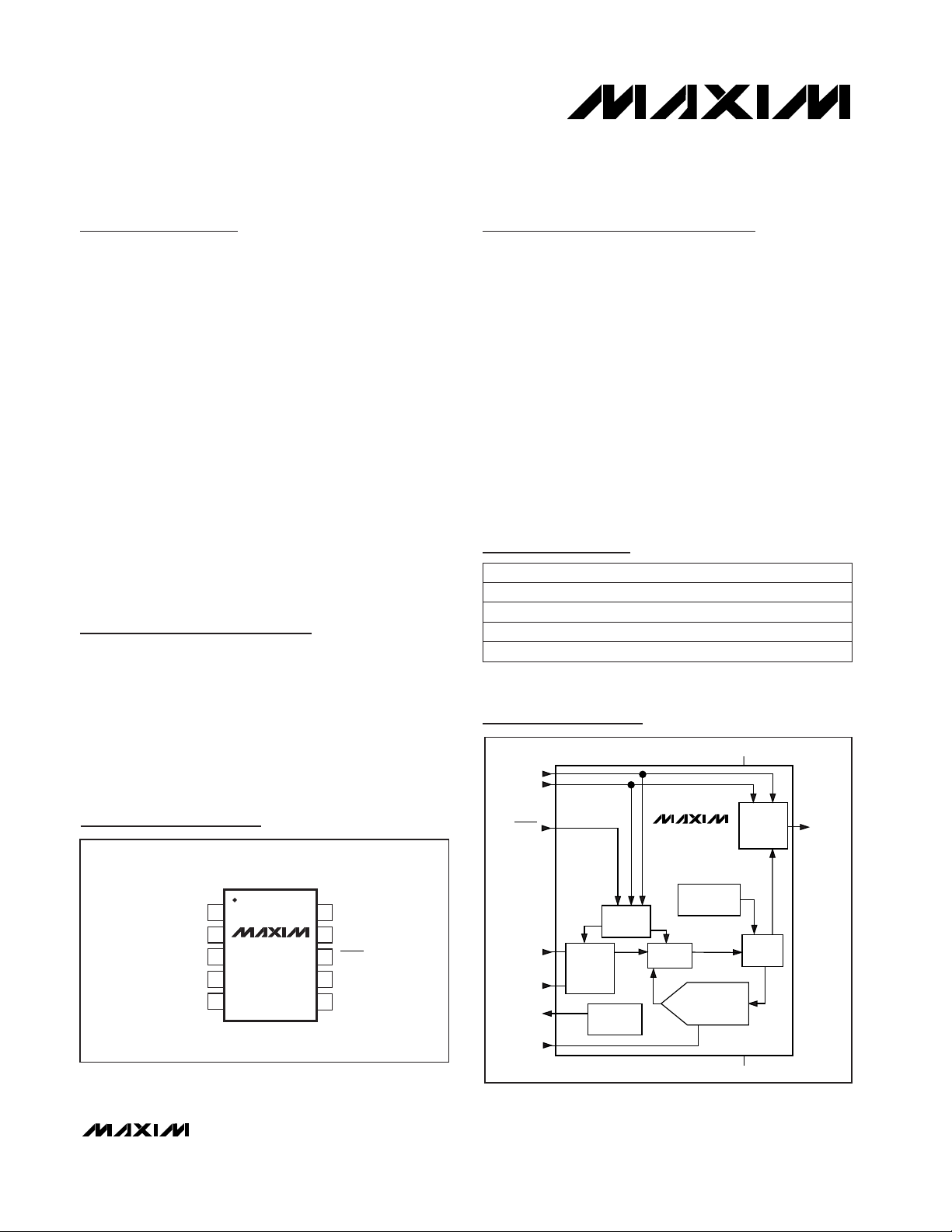
1
2
3
4
5
10
9
8
7
6
SCLK
DOUT
SHDN
CONVSTGND
IN-
IN+
V
DD
MAX1106
MAX1107
µMAX
TOP VIEW
REFINREFOUT
Functional Diagram
19-1432; Rev 0; 3/99
Pin Configuration
Ordering Information
PART
MAX1106CUB
MAX1106EUB -40°C to +85°C
0°C to +70°C
TEMP. RANGE PIN-PACKAGE
10 µMAX
10 µMAX
MAX1107CUB
MAX1107EUB -40°C to +85°C
0°C to +70°C 10 µMAX
10 µMAX
SPI and QSPI are trademarks of Motorola, Inc.
MICROWIRE is a trademark of National Semiconductor Corp.
V
DD
CONVST
SCLK
OUTPUT
SHDN
MAX1106
MAX1107
SHIFT
REGISTER
DOUT
INTERNAL
CONTROL
LOGIC
IN+
IN-
REFOUT
REFIN
ANALOG
INPUT
MUX
REFERENCE
INTERNAL
OSCILLATOR
T/H
CHARGE
REDISTRIBUTION
DAC
SAR
GND
MAX1106/MAX1107
Single-Supply, Low-Power,
Serial 8-Bit ADCs
2 _______________________________________________________________________________________
ABSOLUTE MAXIMUM RATINGS
ELECTRICAL CHARACTERISTICS—MAX1106
(VDD= +2.7V to +3.6V; IN- to GND; f
SCLK
= 2MHz; 25ksps conversion rate; 1µF capacitor at REFOUT; external +2.048V reference at
REFIN; T
A
= T
MIN
to T
MAX
; unless otherwise noted. Typical values are at TA= +25°C.)
Stresses beyond those listed under “Absolute Maximum Ratings” may cause permanent damage to the device. These are stress ratings only, and functional
operation of the device at these or any other conditions beyond those indicated in the operational sections of the specifications is not implied. Exposure to
absolute maximum rating conditions for extended periods may affect device reliability.
VDDto GND..............................................................-0.3V to +6V
IN+, IN-, REFIN, REFOUT,
DOUT to GND..........................................-0.3V to (V
DD
+ 0.3V)
SHDN, SCLK, CONVST to GND...............................-0.3V to +6V
Continuous Power Dissipation (T
A
= +70°C)
10-pin µMAX (derate 5.6mW/°C above +70°C)............444mW
Operating Temperature Ranges
MAX110_CUB......................................................0°C to +70°C
MAX110_EUB ...................................................-40°C to +85°C
Storage Temperature Range.............................-65°C to +150°C
Lead Temperature (soldering, 10sec).............................+300°C
V
DD
= 2.7V to 3.6V
VDD= 5.5V (Note 2)
No missing codes over temperature
CONDITIONS
±0.15 ±0.5
Bits8Resolution
LSB
±0.2
INLRelative Accuracy (Note 1)
LSB±1DNLDifferential Nonlinearity
UNITSMIN TYP MAXSYMBOLPARAMETER
VDD= 5.5V (Note 2)
VDD= 2.7V to 3.6V
LSB
±0.5
Offset Error
±0.2 ±1
LSB±1Gain Error (Note 3)
ppm/°C±0.8Gain Temperature Coefficient
TA= T
MIN
to T
MAX
TA= +25°C
dB49SINADSignal-to-Noise Plus Distortion
dB-70THD
Total Harmonic Distortion
(up to the 5th harmonic)
LSB
±0.5
TUETotal Unadjusted Error
±1
-3dB rolloff
V
IN+
to V
IN-
MHz0.8Full-Power Bandwidth
MHz1.5BW
-3dB
Small-Signal Bandwidth
0V
REFIN
Input Voltage Range (Note 4)
dB68SFDRSpurious-Free Dynamic Range
VV
IN_
pF18C
IN
Input Capacitance
On/off-leakage current,
V
IN+
or V
IN-
= 0 or V
DD
µA±0.01 ±1Input Leakage Current
DC ACCURACY
DYNAMIC PERFORMANCE (10kHz sine-wave input, 2.048Vp-p, 25ksps conversion rate)
ANALOG INPUTS
V
MAX1106/MAX1107
Single-Supply, Low-Power,
Serial 8-Bit ADCs
_______________________________________________________________________________________ 3
ELECTRICAL CHARACTERISTICS—MAX1106 (continued)
(VDD= +2.7V to +3.6V; IN- to GND; f
SCLK
= 2MHz; 25ksps conversion rate; 1µF capacitor at REFOUT; external +2.048V reference at
REFIN; T
A
= T
MIN
to T
MAX
; unless otherwise noted. Typical values are at TA= +25°C.)
CONDITIONS UNITSMIN TYP MAXSYMBOLPARAMETER
Figure 7 µst
CONV
Conversion Time 35
µs1t
ACQ
Track/Hold Acquisition Time
ps<50Aperture Jitter
ns10Aperture Delay
kHz400Internal Clock Frequency
(Note 5)
0 to 0.5mA (Note 6)
ppm/°C±50REF Tempco
µA150I
REFSC
REF Short-Circuit Current
mV4Load Regulation
V1.968 2.048 2.128V
REFOUT
Output Voltage
+2.048V at REFIN, full scale µA120Input Current
V2.7 3 5.5V
DD
Supply Voltage
Power down, VDD= 3.6V
Full-scale input, VDD= 2.7V to 3.6V
0.5 2.5
I
DD
mV±0.4 ±4PSRPower-Supply Rejection (Note 8)
VDD= 3.6V, CL= 10pF
VDD= 5.5V, CL= 10pF 115
µF1Capacitive Bypass at REFOUT
V0.2V
HYST
Input Hysteresis
V0.8V
IL
Threshold Voltage Low
µA±1I
IH
Input Current High
VDD≤ 3.6V
VDD> 3.6V
2
V
3
V
IH
Threshold Voltage High
MHz2External Clock Frequency Range
V1.0 VDD+ 0.05V
REFIN
Input Voltage Range
µA±1I
IL
Input Current Low
pF15C
IN
Input Capacitance
For data transfer only
96 250
µASupply Current (Notes 2, 7)
TRACK/HOLD
INTERNAL REFERENCE
EXTERNAL REFERENCE
POWER REQUIREMENTS
DIGITAL INPUTS (SHDN, SCLK, and CONVST)
V
MAX1106/MAX1107
Single-Supply, Low-Power,
Serial 8-Bit ADCs
4 _______________________________________________________________________________________
Figure 6, DOUT High-Z
Figure 6, DOUT High-Z
pF15C
OUT
Three-State Output Capacitance
µA±0.01 ±10I
L
Three-State Leakage Current
Figure 1, C
LOAD
= 100pF
Figure 1, C
LOAD
= 100pF
ns20 200t
DO
SCLK Fall to Output Data Valid
ns
CONDITIONS
240t
DV
CONVST Rise to Output Enable
ns200t
CH
SCLK Pulse Width High
µs1t
CSPW
CONVST Pulse Width High
µs1t
ACQ
Acquisition Time
µs35t
CONV
CONVST Fall to Output Data
Valid
External reference
Figure 2, C
LOAD
= 100pF
Internal reference (Note 9)
µs20
ns240t
SHDN
SHDN Fall to Output Disable
ms12
t
WAKE
Wake-Up Time
Figure 2, C
LOAD
= 100pF ns240t
TR
SCLK Low to Output Disable
ns200t
CL
SCLK Pulse Width Low
ns100t
SCC
SCLK Low to CONVST Rise
UNITSMIN TYP MAXSYMBOLPARAMETER
I
SINK
= 5mA
I
SOURCE
= 0.5mA
I
SINK
= 16mA
0.4
VVDD- 0.5V
OH
Output High Voltage
V
0.8
V
OL
Output Low Voltage
ELECTRICAL CHARACTERISTICS—MAX1106 (continued)
(VDD= +2.7V to +3.6V; IN- to GND; f
SCLK
= 2MHz; 25ksps conversion rate; 1µF capacitor at REFOUT; external +2.048V reference at
REFIN; T
A
= T
MIN
to T
MAX
; unless otherwise noted. Typical values are at TA= +25°C.)
DIGITAL OUTPUT (DOUT)
TIMING CHARACTERISTICS (Figures 6 and 7)
MAX1106/MAX1107
Single-Supply, Low-Power,
Serial 8-Bit ADCs
_______________________________________________________________________________________ 5
ELECTRICAL CHARACTERISTICS—MAX1107
(VDD= +4.5V to +5.5V; IN- = GND; f
SCLK
= 2MHz; 25ksps conversion rate; 1µF capacitor at REFOUT; external +4.096V reference at
REFIN; T
A
= T
MIN
to T
MAX
; unless otherwise noted. Typical values are at TA= +25°C.)
ps<50Aperture Jitter
ns10Aperture Delay
kHz400Internal Clock Frequency
0 to 0.5mA (Note 6)
ppm/°C±50REF Tempco
mA
CONDITIONS
5I
REFSC
REF Short-Circuit Current
mV4Load Regulation
MHz
V3.936 4.096 4.256V
REFOUT
Output Voltage
µF1Capacitive Bypass at REFOUT
UNITSMIN TYP MAXSYMBOLPARAMETER
dBSINADSignal-to-Noise Plus Distortion 49
µs1t
ACQ
Track/Hold Acquisition Time
Figure 7 µst
CONV
Conversion Time 35
SFDRSpurious-Free Dynamic Range dB
dB
68
THD
Total Harmonic Distortion
(up to the 5th harmonic)
-70
Full-Power Bandwidth MHz
V
IN+
to V
IN-
0V
REFIN
-3dB rolloff MHz
0.8
BW
-3dB
Small-Signal Bandwidth 1.5
V
IN_
Input Voltage Range (Note 4) V
Input Leakage Current µA
On/off-leakage current,
V
IN+
or V
IN-
= 0 or V
DD
±0.01 ±1
pFC
IN
Input Capacitance 18
2External Clock Frequency Range For data transfer only
TA= T
MIN
to T
MAX
±0.5
TA= +25°C
LSB
±1
TUETotal Unadjusted Error
ppm/°C±0.8Gain Temperature Coefficient
LSB±1Gain Error (Note 3)
LSB±0.2 ±1Offset Error
No missing codes over temperature LSB±1DNLDifferential Nonlinearity
LSB±0.15 ±0.5INLRelative Accuracy (Note 1)
Bits8Resolution
DC ACCURACY
DYNAMIC PERFORMANCE (10kHz sine-wave input, 4.096Vp-p, 25ksps conversion rate)
ANALOG INPUTS
TRACK/HOLD
INTERNAL REFERENCE

MAX1106/MAX1107
Single-Supply, Low-Power,
Serial 8-Bit ADCs
6 _______________________________________________________________________________________
ELECTRICAL CHARACTERISTICS—MAX1107 (continued)
(VDD= +4.5V to +5.5V; IN- = GND; f
SCLK
= 2MHz; 25ksps conversion rate; 1µF capacitor at REFOUT; external +4.096V reference at
REFIN; T
A
= T
MIN
to T
MAX
; unless otherwise noted. Typical values are at TA= +25°C.)
Figure 6, DOUT High-Z
Figure 6, DOUT High-Z
pF15C
OUT
Three-State Output Capacitance
µA±0.01 ±10I
L
Three-State Leakage Current
Figure 1, C
LOAD
= 100pF
Figure 1, C
LOAD
= 100pF
ns20 200t
DO
SCLK Fall to Output Data Valid
ns
CONDITIONS
240t
DV
CONVST Rise to Output Enable
ns200t
CH
SCLK Pulse Width High
µs1t
CSPW
CONVST Pulse Width High
µs1t
ACQ
Acquisition Time
µs35t
CONV
CONVST Fall to Output Data
Valid
UNITSMIN TYP MAXSYMBOLPARAMETER
I
SINK
= 5mA
I
SINK
= 16mA
0.4
V4.5 5 5.5V
DD
Supply Voltage
V
0.8
V
OL
Output Low Voltage
VDD= 5.5V, CL= 10pF,
full-scale input
115 250
Power down, VDD= 4.5V to 5.5V 0.5 2.5
External reference = 4.096V,
full-scale input, V
DD
= 4.5V to 5.5V
mV±0.4 ±4PSRPower-Supply Rejection (Note 8)
V0.2V
HYST
Input Hysteresis
V0.8V
IL
Threshold Voltage Low
V3V
IH
Threshold Voltage High
µA±1I
IH
Input Current High
pF15C
IN
Input Capacitance
I
SOURCE
= 0.5mA VVDD- 0.5V
OH
Output High Voltage
µA±1I
IL
Input Current Low
µAI
DD
Supply Current (Notes 2, 7)
4.096V at REFIN, full scale µA120Input Current
V1.0 VDD+ 0.05V
REFIN
Input Voltage Range
EXTERNAL REFERENCE
DIGITAL INPUTS (SHDN, SCLK, and CONVST)
DIGITAL OUTPUT (DOUT)
TIMING CHARACTERISTICS (Figures 6 and 7)
POWER REQUIREMENTS

MAX1106/MAX1107
Single-Supply, Low-Power,
Serial 8-Bit ADCs
_______________________________________________________________________________________ 7
ELECTRICAL CHARACTERISTICS—MAX1107 (continued)
(VDD= +4.5V to +5.5V; IN- = GND; f
SCLK
= 2MHz; 25ksps conversion rate; 1µF capacitor at REFOUT; external +4.096V reference at
REFIN; T
A
= T
MIN
to T
MAX
; unless otherwise noted. Typical values are at TA= +25°C.)
CONDITIONS
External reference
Figure 2, C
LOAD
= 100pF
Internal reference (Note 9)
µs20
ns240t
SHDN
SHDN Fall to Output Disable
ms12
t
WAKE
Wake-Up Time
Figure 2, C
LOAD
= 100pF ns240t
TR
SCLK Low to Output Disable
ns200t
CL
SCLK Pulse Width Low
ns100t
SCC
SCLK Low to CONVST Rise
UNITSMIN TYP MAXSYMBOLPARAMETER
Note 1: Relative accuracy is the deviation of the analog value at any code from its theoretical value after the full-scale range has
been calibrated.
Note 2: See
Typical Operating Characteristics
.
Note 3: V
REFOUT
= +2.048V (MAX1106), V
REFOUT
= +4.096V (MAX1107), offset nulled.
Note 4: Common-mode range (IN+, IN-) GND to V
DD
.
Note 5: REFOUT supplies typically 2.5mA under normal operating conditions.
Note 6: External load should not change during the conversion for specified accuracy.
Note 7: Power consumption with CMOS levels.
Note 8: Measured as
VFS(2.7V) - VFS(3.6V) for MAX1106, and measured as VFS(4.5V) - VFS(5.5V) for MAX1107.
Note 9: 1µF at REFOUT, internal reference settling to 0.5LSB.
Typical Operating Characteristics
(VDD= +3.0V (MAX1106), VDD= +5.0V (MAX1107); f
SCLK
= 2MHz; 25ksps conversion rate; external reference; 1µF at REFOUT;
TA= +25°C; unless otherwise noted.)
200
50
2.5 5.5
SUPPLY CURRENT vs. SUPPLY VOLTAGE
75
175
MAX1106/07-01
SUPPLY VOLTAGE (V)
SUPPLY CURRENT (µA)
3.0 3.5 4.0 4.5 5.0
150
125
100
C
LOAD
= 10pF
DOUT = 10101010
C
LOAD
= 10pF
DOUT = 11111111
C
LOAD
= 47pF
DOUT = 10101010
MAX1106 (V
DD
= 2.7V TO 5.5V)
MAX1107 (V
DD
= 4.5V TO 5.5V)
INTERNAL REFERENCE
200
50
-40 100
SUPPLY CURRENT vs. TEMPERATURE
75
175
MAX1106/07-02
TEMPERATURE (°C)
SUPPLY CURRENT (µA)
-200 20406080
150
125
100
DOUT = 10101010
C
LOAD
= 10pF
INTERNAL REFERENCE
MAX1107, V
DD
= 5.0V
MAX1106, V
DD
= 3.0V
0.50
0
2.5 5.5
SHUTDOWN SUPPLY CURRENT
vs. SUPPLY VOLTAGE
0.10
0.05
0.45
0.40
MAX1106/07-03
SUPPLY VOLTAGE (V)
SHUTDOWN SUPPLY CURRENT (µA)
3.0 3.5 4.0 4.5 5.0
0.35
0.30
0.25
0.20
0.15

MAX1106/MAX1107
Single-Supply, Low-Power,
Serial 8-Bit ADCs
8 _______________________________________________________________________________________
Typical Operating Characteristics (continued)
(VDD= +3.0V (MAX1106), VDD= +5.0V (MAX1107); f
SCLK
= 2MHz; 25ksps conversion rate; external reference; 1µF at REFOUT;
TA= +25°C; unless otherwise noted.)
0.5
-0.5
2.5 5.5
OFFSET ERROR vs. SUPPLY VOLTAGE
-0.3
-0.4
0.4
0.3
MAX1106/07-04
SUPPLY VOLTAGE (V)
OFFSET ERROR (LSB)
3.0 3.5 4.0 4.5 5.0
0.2
0.1
0
-0.1
-0.2
0.5
-0.5
-40 100
OFFSET ERROR vs. TEMPERATURE
-0.3
-0.4
0.4
0.3
MAX1106/07-05
TEMPERATURE (°C)
OFFSET ERROR (LSB)
-200 20406080
0.2
0.1
0
-0.1
-0.2
0.20
-0.20
0 5.0
OFFSET ERROR vs. REFERENCE VOLTAGE
-0.10
-0.15
0.15
0.10
MAX1106/07-06
REFERENCE VOLTAGE (V)
OFFSET ERROR (LSB)
0.5 1.0 1.5 2.0 2.5 3.0 3.5 4.0 4.5
0.05
0
-0.05
0.5
-0.5
2.5 5.5
GAIN ERROR vs. SUPPLY VOLTAGE
-0.3
-0.4
0.4
0.3
MAX1106/07-07
SUPPLY VOLTAGE (V)
GAIN ERROR (LSB)
3.0 3.5 4.0 4.5 5.0
0.2
0.1
0
-0.1
-0.2
0.3
-0.3
2.5 5.5
INTEGRAL NONLINEARITY
vs. SUPPLY VOLTAGE
-0.1
-0.2
0.2
MAX1106/07-10
SUPPLY VOLTAGE (V)
INL (LSB)
3.0 3.5 4.0 4.5 5.0
0.1
0
1.0
-1.0
-40 100
GAIN ERROR vs. TEMPERATURE
-0.6
-0.8
0.8
0.6
MAX1106/07-08
TEMPERATURE (°C)
GAIN ERROR (LSB)
-200 20406080
0.4
0.2
0
-0.2
-0.4
1.0
-1.0
0 5.0
GAIN ERROR vs. REFERENCE VOLTAGE
-0.4
-0.6
-0.8
0.8
0.6
MAX1106/07-09
REFERENCE VOLTAGE (V)
GAIN ERROR (LSB)
0.5 1.0 1.5 2.0 2.5 3.0 3.5 4.0 4.5
0.4
0
0.2
-0.2
0.5
-0.5
0 300
DIFFERENTIAL NONLINEARITY
vs. DIGITAL CODE
-0.1
0
-0.3
-0.4
-0.2
0.4
0.3
MAX1106/07-11
DIGITAL CODE
DNL (LSB)
50 100 150 200 250
0.1
0.2
0.5
-0.5
2.5 5.5
DIFFERENTIAL NONLINEARITY
vs. SUPPLY VOLTAGE
-0.2
-0.3
-0.4
0.4
0.3
MAX1106/07-12
SUPPLY VOLTAGE (V)
DNL (LSB)
3.0 3.5 4.0 4.5 5.0
0.2
0.1
0
-0.1

MAX1106/MAX1107
Single-Supply, Low-Power,
Serial 8-Bit ADCs
_______________________________________________________________________________________
9
0.5
-0.5
0 300
INTEGRAL NONLINEARITY
vs. DIGITAL CODE
-0.1
0
-0.3
-0.4
-0.2
0.4
0.3
MAX1106/07-13
DIGITAL CODE
INL (LSB)
50 100 150 200 250
0.1
0.2
20
-100
014
FFT PLOT
-60
-80
0
MAX1106/07-14
FREQUENCY (kHz)
AMPLITUDE (dB)
24681012
-20
-40
f
IN+
= 10.34kHz, 2Vp-p
f
SAMPLE
= 25088Hz
21.5
18.5
06
CONVERSION TIME vs. SUPPLY VOLTAGE
19.5
19.0
21.0
MAX1106/07-15
SUPPLY VOLTAGE (V)
CONVERSION TIME (µs)
12345
20.5
20.0
Typical Operating Characteristics (continued)
(VDD= +3.0V (MAX1106), VDD= +5.0V (MAX1107); f
SCLK
= 2MHz; 25ksps conversion rate; external reference; 1µF at REFOUT;
TA= +25°C; unless otherwise noted.)
Pin Description
Positive Analog Input. Sampled. Input range from GND to VDD.IN+2
Ground.GND4
Negative Analog Input. Input range from GND to VDD.IN-3
Reference Voltage Input. Reference voltage for analog-to-digital conversion. Connect REFOUT to REFIN
for internal reference. Input range from 1V to VDD.
REFIN6
Active-Low Shutdown. Connect to VDDfor normal operation.
SHDN
8
Conversion Start Input. Toggle CONVST high for 1µs minimum and then low to start internal conversion.
Data is not clocked out unless CONVST is low.
CONVST7
Internal Reference Output. Bypass with 1µF to ground. 2.048V for MAX1106, 4.096V for MAX1107.REFOUT5
Serial Data Output. Data is clocked out on the falling edge of SCLK. DOUT is high impedance in shutdown
or after all data is clocked out.
DOUT9
PIN
Positive Supply VoltageV
DD
1
FUNCTIONNAME
Serial Clock Input. Clocks data out of serial interface.SCLK10
CONVERSION TIME vs. TEMPERATURE
25
24
23
22
21
20
19
18
CONVERSION TIME (µs)
17
16
15
-40 100
-20 0 20 40 60 80
VDD = 3V
TEMPERAT
VDD = 5V
RE
°
NORMALIZED REFERENCE VOLTAGE
vs. TEMPERATURE
1.0010
MAX1106/07-16
1.0005
1.0000
0.9995
0.9990
NORMALIZED REFERENCE VOLTAGE
0.9985
0.9980
-20 0 20 40 60 80
-40 100
TEMPERATURE (°C)
MAX1106/07-17

MAX1106/MAX1107
Single-Supply, Low-Power,
Serial 8-Bit ADCs
10 ______________________________________________________________________________________
_______________Detailed Description
The MAX1106/MAX1107 analog-to-digital converters
(ADCs) use a successive-approximation conversion
technique and input track/hold (T/H) circuitry to convert
an analog signal to an 8-bit digital output. A simple serial interface provides easy interface to microprocessors
(µPs). No external hold capacitors are required. All of
the MAX1106/MAX1107 operating modes are pin configurable: internal or external reference, single-ended
or pseudo-differential unipolar conversion, and power
down. Figure 3 shows the typical operating circuit.
Analog Inputs
Track/Hold
The input architecture of the ADCs is illustrated in
Figure 4’s equivalent-input circuit of and is composed
of the T/H, the input multiplexer, the input comparator,
the switched capacitor DAC, and the auto-zero rail.
The device is in acquisition mode most of the time.
During the acquisition interval, the positive input (IN+)
is tracked and is connected to the holding capacitor
(C
HOLD
). The acquisition interval ends with the falling
edge of CONVST. At this point the T/H switch opens
and C
HOLD
is connected to the negative input (IN-),
retaining charge on C
HOLD
as a sample of the signal at
IN+. Once conversion is complete the T/H returns
immediately to its tracking mode.
The time required for the T/H to acquire an input signal
is a function of how quickly its input capacitance is
charged. If the input signal’s source impedance is high,
the acquisition time lengthens, and more time must be
allowed between conversions. The acquisition time,
t
ACQ
, is the minimum time needed for the signal to be
acquired. It is calculated by:
t
ACQ
= 6(RS+ RIN)18pF
VDD
3k
C
LOAD
GND
DOUT
C
LOAD
GND
3k
DOUT
a) V
OL
to V
OH
b) High-Z to VOL and VOH to V
OL
Figure 1. Load Circuits for Enable Time
V
DD
3k
C
LOAD
GND
DOUT
C
LOAD
GND
3k
DOUT
a) V
OH
to High-Z b) VOL to High-Z
Figure 2. Load Circuits for Disable Time
V
DD
I/O
SCK (SK)
MISO (SI)
GND
DOUT
SCLK
CONVST
GND
SHDN
V
DD
IN-
1µF
0.1µF
1µF
ON
OFF
IN+
ANALOG
INPUTS
MAX1106
MAX1107
CPU
V
DD
REFOUT
REFIN
Figure 3. Typical Operating Circuit
IN-
IN+
REFIN
GND
C
HOLD
CAPACITIVE DAC
COMPARATOR
18pF
R
IN
6.5k
AUTOZERO
RAIL
TRACK
HOLD
Figure 4. Equivalent Input Circuit

MAX1106/MAX1107
Single-Supply, Low-Power,
Serial 8-Bit ADCs
______________________________________________________________________________________ 11
where RIN= 6.5kΩ, RS= the source impedance of the
input signal, and t
ACQ
must never be less than 1µs.
This is easily achieved by respecting the minimum
CONVST high interval required and the time required to
clock the data out.
Pseudo-Differential Input
The MAX1106/MAX1107 input configuration is pseudodifferential to the extent that only the signal at the sampled input (IN+) is stored in the holding capacitor
(C
HOLD
). IN- must remain stable within ±0.5LSB
(±0.1LSB for best results) in relation to GND during a
conversion.
If a varying signal is applied at the IN- input, its amplitude and frequency need to be limited. The following
equations determine the relationship between the maximum signal amplitude and its frequency to maintain
±0.5LSB accuracy:
Assuming a sinusoidal signal at the IN- input,
under the maximum voltage variation is determined by
a 60Hz signal at IN- with an amplitude of 1.2V will
generate ±0.5LSB of error. This is with a 35µs conversion time (maximum t
CONV
) and a reference voltage of
4.096V. When a DC reference voltage is used at IN-,
connect a 0.1µF capacitor from IN_ to GND to minimize
noise at the input.
The common-mode input range of IN+ and IN- is GND
to +VDD. Full-scale is achieved when (V
IN-
- V
IN+
) =
V
REFIN
. V
IN+
must be higher than V
IN-
.
Conversion Process
The comparator negative input is connected to the autozero rail. Since the device requires only a single supply,
the ZERO node at the input of the comparator equals
VDD/2. The capacitive DAC restores node ZERO to have
0V difference at the comparator inputs within the limits
of 8-bit resolution. This action is equivalent to transferring a charge of 18pF(V
IN+
- V
IN-
) from C
HOLD
to the
binary-weighted capacitive DAC which, in turn, forms a
digital representation of the analog-input signal.
Input Voltage Range
Internal protection diodes that clamp the analog input to
VDDand GND allow the input pins (IN+ and IN-) to swing
from (GND - 0.3V) to (V
DD
+ 0.3V) without damage.
However, for accurate conversions, the inputs must not
exceed (VDD+ 50mV) or be less than (GND - 50mV).
The MAX1106/MAX1107 input range is from GND to
VDD. The output code is invalid (code zero) when a
negative input voltage (or a negative differential input
voltage) is applied. The reference input-voltage range
at REFIN is from 1V to (V
DD
+ 50mV).
Input Bandwidth
The ADC’s input tracking circuitry has a 1.5MHz smallsignal bandwidth, so it is possible to digitize highspeed transient events and measure periodic signals
with bandwidths exceeding the ADC’s sampling rate by
using undersampling techniques. To avoid high-frequency signals being aliased into the frequency band
of interest, anti-alias filtering is recommended.
Serial Interface
The MAX1106/MAX1107 have a 3-wire serial interface.
The CONVST and SCLK inputs are used to control the
device, while the three-state DOUT pin is used to
access the result of conversion.
The serial interface provides easy connection to microcontrollers with SPI, QSPI, and MICROWIRE serial interfaces at clock rates up to 2MHz. For SPI and QSPI, set
CPOL = CPHA = 0 in the SPI control registers of the
microcontroller. Figure 5 shows the MAX1106/MAX1107
common serial-interface connections.
Digital Inputs and Outputs
The logic levels of the MAX1106/MAX1107 digital
inputs are set to accept voltage levels from both 3V
and 5V systems regardless of the supply voltages.
A conversion is started by toggling CONVST. CONVST
idles low and needs to be set high for at least 1µs to
perform the autozero adjustment. CONVST must remain
low during conversion and until the result of conversion
has been clocked out.
After CONVST is set low, allow 35µs for the conversion
to be completed. While the internal conversion is in
progress DOUT is low. Conversion is controlled by an
internal 400kHz oscillator. The MSB is present at the
DOUT pin immediately after conversion is completed.
The conversion result is clocked out at the DOUT pin
and is coded in straight binary (Figure 9). Data is
clocked out at SCLK’s falling edge in MSB-first format
at rates up to 2MHz. Once all data bits are clocked out,
DOUT goes high impedance at the falling edge of the
eighth SCLK pulse.
max
t
2fV
1 LSB
t
V
2t
IN-
IN-
CONV
REFIN
8
CONV
∆∆υ
=
()
≤=π
υ
IN- IN-
V sin(2 ft)=
()
π

Starting SCLK before conversion is complete corrupts
the conversion in progress, and the data clocked out at
DOUT does not represent the input signal. Bringing
CONVST high at anytime during a conversion or while
the data is clocked out will result in an incorrect conversion. A new conversion can be restarted only if all eight
data bits of conversion have been clocked out. Toggle
CONVST after all data is clocked out to restart a new
conversion.
SHDN is used to place the MAX1106/MAX1107 in lowpower mode (see
Power-Down
section). In this mode
DOUT is high impedance and any conversion in
progress is stopped immediately. If a conversion is
stopped by SHDN going low, the device must be reset
by waiting 35µs and clearing the output register with
eight SCLKs before the next conversion.
How to Perform a Conversion
The MAX1106/MAX1107 converts an input signal using
the internal clock. This frees the µP from the burden of
running the SAR conversion clock, and allows the conversion results to be read back at the µP’s convenience
at any clock rate up to 2MHz.
Figures 6 and 7 show the serial interface timing characteristics. CONVST idles low. Toggle CONVST high for at
least 1µs to perform the autozero adjustment. After
CONVST goes low, conversion starts immediately.
Allow 35µs for the internal conversion to complete and
issue the MSB of the conversion at DOUT. CONVST
needs to be held low once a conversion is started,
while SCLK should remain low during conversion for
best noise performance. An internal register stores data
when the conversion is in progress. SCLK clocks the
CONVST
SCLK
1µs
(MIN)
HIGH-Z
HIGH-Z
DOUT
18
100µs (MAX)
D7
MSB
LSB
D6 D5 D4 D3 D2 D1 D0
t
CONV
= 35µs (MAX)
CONVERSION
ACQUISITION
t
CSPW
A/D STATE
ACQ
Figure 6. Conversion Timing Diagram
MAX1106/MAX1107
Single-Supply, Low-Power,
Serial 8-Bit ADCs
12 ______________________________________________________________________________________
CONVST
SCLK
DOUT
I/O
SCK
MISO
+3V
SS
a) SPI
CONVST
CONVST
SCLK
DOUT
CS
SCK
MISO
+3V
SS
b) QSPI
MAX1106
MAX1107
MAX1106
MAX1107
MAX1106
MAX1107
SCLK
DOUT
I/O
SK
SI
c) MICROWIRE
Figure 5. Common Serial-Interface Connections

MAX1106/MAX1107
Single-Supply, Low-Power,
Serial 8-Bit ADCs
______________________________________________________________________________________ 13
data out of this register at any time after the conversion
is complete. After the eighth data-bit has clocked out,
DOUT goes high impedance and remains so with additional SCLKs.
Normally leave CONVST low until a new conversion
needs to be started. CONVST should be high for a
maximum of 100µs to maintain the 8-bit accuracy of the
Autozero Circuit.
The acquisition time, t
ACQ
, starts immediately after the
end of conversion and a new conversion can be started
immediately after all data has been clocked out by toggling CONVST high. Figure 8 shows a timing diagram
for a conversion at the data rate of 40ksps. Typically
20µs are necessary for the conversion to complete, 4µs
for reading the eight bits of data with a serial clock of
2MHz, and 1µs to complete the zero rail adjustment
and acquisition. The conversion time is guaranteed to
be less than 35µs, therefore the data rate should be
limited to 25ksps unless the conversion time for the
specific condition is known. Conversion time can be
determined by measuring the time between CONVST
falling edge and DOUT rising edge with a full-scale
input voltage.
__________Applications Information
Power-On Reset
When power is first applied with SHDN high or connected to VDD, the MAX1106/MAX1107 is in track mode.
Conversion can be started by toggling CONVST high to
low as soon as the reference is settled when using the
internal reference, or after 20µs when an external reference is used. Powering up the MAX1106/MAX1107 with
CONVST low will not start a conversion. No conversions
should be performed until the reference voltage (internal or external) has stabilized.
Shutdown Operation
Pulling SHDN low places the converter in low-current
power-down mode. In this state the converter draws
typically 0.5µA. In shutdown the analog biasing circuit
and the internal bandgap reference are powered down,
and DOUT goes high impedance.
The conversion stops coincidentally with SHDN going
low. If shutdown occurs during a conversion, power up,
wait 35µs, and clock SCLK eight times.
CONVST
SCLK
DOUT
t
CSPW
t
CONV
t
DV
t
CH
#1
#8
t
CL
t
DO
t
DV
t
TR
t
SCC
Figure 7. Detailed Serial Interface Timing
CONVST
5V/div
SCLK
5V/div
DOUT
5V/div
5µs/div
t
CONV
Figure 8. 40ksps Timing Diagram
MAX1106/MAX1107
Single-Supply, Low-Power,
Serial 8-Bit ADCs
14 ______________________________________________________________________________________
When operating at speeds below the maximum sampling rate, the MAX1106/MAX1107’s power-down mode
can save considerable power by placing the converter
in a low-current shutdown state between conversions.
Pull SHDN low after the conversion byte has been read
to shut down the device completely.
CONVST should remain low most of the time and toggled high for 1µs (100µs max) for the autozero adjustment. An external reference is recommended for best
accuracy when using the shutdown feature. This
requires only 20µs for the internal biasing circuit to stabilize before starting a new conversion. Alternatively,
the internal reference can be used, but additional time
is required for the reference to stabilize (when
bypassed by a 1µF capacitor; at data rates above
1ksps, the reference stabilizes within 1LSB in 200µs). If
the reference is completely discharged it requires
12ms to settle. No conversions should be performed
until the reference voltage has stabilized.
Internal or External Voltage Reference
An external reference between 1V and VDDshould be
connected directly at the REFIN pin. To use the internal
reference, connect REFOUT directly to REFIN and
bypass REFOUT with a 1µF capacitor. The DC input
impedance at REFIN is extremely high, consisting of
leakage current only (typically 10nA). During a conversion, the reference must be able to deliver up to 20µA
average load current and have an output impedance of
1kΩ or less at the conversion clock frequency. If the
reference has higher output impedance or is noisy,
bypass it close to the REFIN pin with a 0.1µF capacitor.
The internal reference is active as long as SHDN is high
and powers down when SHDN is low.
Transfer Function
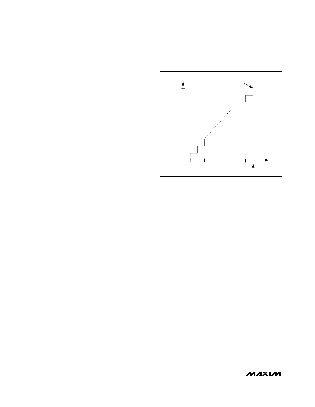
Figure 9 depicts the input/output transfer function.
Code transitions occur at integer LSB values. Output
coding is binary; with a 2.048V reference 1LSB = 8mV
(V
REFIN
/ 256). For single-ended operation connect IN-
to GND. Full-scale is achieved at V
IN+
= V
REFIN
- 1LSB.
For pseudo-differential operation the V
IN-
voltage range
is from GND to VDD, where full-scale is achieved at
V
IN+
= V
REFIN
+ V
IN-
- 1LSB. V
IN+
should not be higher
than VDD+ 50mV. Negative input voltages are invalid
and give a zero output code. Voltages greater than fullscale give an all ones output code.
OUTPUT CODE
FULL-SCALE
TRANSITION
11111111
11111110
11111101
00000011
00000010
00000001
00000000
123
0
FS
FS - 1LSB
FS = V
REFIN
+ V
IN-
1LSB = V
REFIN
256
INPUT VOLTAGE (LSB)
(IN-)
Figure 9. Input/Output Transfer Function

MAX1106/MAX1107
Single-Supply, Low-Power,
Serial 8-Bit ADCs
______________________________________________________________________________________ 15
Layout, Grounding, and Bypassing
For best performance, use printed circuit boards. Wirewrap boards are not recommended. Board layout
should ensure that digital and analog signal lines are
separated from each other. Do not run analog and digital (especially clock) lines parallel to one another or run
digital lines underneath the ADC package.
Figure 10 shows the recommended system-ground
connections. A single-point analog ground (star-ground
point) should be established at the A/D ground.
Connect all analog grounds to the star ground. No digital-system ground should be connected to this point.
The ground return to the power supply for the star
ground should be low impedance and as short as possible for noise-free operation.
High-frequency noise in the VDDpower supply may
affect the comparator in the ADC. Bypass the supply to
the star ground with 0.1µF and 1µF capacitors close to
the VDDpin of the MAX1106/MAX1107. Minimize
capacitor lead lengths for best supply-noise rejection. If
the power supply is very noisy, a 10Ω resistor can be
connected to form a lowpass filter.
GND
+3V/+5V
SYSTEM POWER SUPPLIES
V
DD
DGNDV
DD
IN-
1µF
10Ω
0.1µF
GND
DIGITAL
CIRCUITRY
MAX1106
MAX1107
Figure 10. Power-Supply Connections
Chip Information
TRANSISTOR COUNT: 2373

MAX1106/MAX1107
Single-Supply, Low-Power,
Serial 8-Bit ADCs
Maxim cannot assume responsibility for use of any circuitry other than circuitry entirely embodied in a Maxim product. No circuit patent licenses are
implied. Maxim reserves the right to change the circuitry and specifications without notice at any time.
16
____________________Maxim Integrated Products, 120 San Gabriel Drive, Sunnyvale, CA 94086 408-737-7600
© 1999 Maxim Integrated Products Printed USA is a registered trademark of Maxim Integrated Products.
Package Information
10LUMAX.EPS
 Loading...