

General Description
The MAX11041 wired remote controller converts up to
30 different pushbuttons into an I2C register. Together
with low-cost pushbutton switches and 1% resistors,
the MAX11041 is a total solution over a single-wire
interface. A wired remote controller easily piggybacks
to a standard 3.5mm headphone jack using a fourth
contact or one of the audio signals.
To conserve battery life, the MAX11041 consumes only
5µA (typ) while reading keypresses in real time without
microprocessor (µP) polling. The device sends the
debounced keypress along with key duration to the
application processor over the I2C interface. An 8-word
FIFO buffer records up to four keypress events to allow
plenty of time for the application processor to respond
to the MAX11041.
The MAX11041 includes ±15kV ESD protection devices
on the FORCE and SENSE inputs to ensure IEC 61000-4-2
compliance without any external ESD devices.
The MAX11041 is available in a 12-pin TQFN package.
The device is specified over the extended temperature
range (-40°C to +85°C).
Applications
Features
o Detect Up to 30 Different Keys and Jack
Insertion/Removal
o Works with Either 32Ω or 16Ω Headphones
o Adds Remote-Control Functionality to Devices
Using a Simple Resistor and Switch Array
o Low-Power Operation Consuming a Supply
Current of Only 5µA (typ)
o Works with Standard 2.5mm or 3.5mm 4-Pin
Headphone Jacks
o Supports Hold Function to Lockout Keys
o 100kHz/400kHz I2C Interface
o Single 1.6V to 3.6V Supply Voltage Range
o ±15kV ESD Protection (IEC 61000-4-2)
MAX11041
Wired Remote Controller
________________________________________________________________
Maxim Integrated Products
1
19-3984; Rev 3; 1/10
For pricing delivery, and ordering information please contact Maxim Direct at 1-888-629-4642,
or visit Maxim’s website at www.maxim-ic.com.
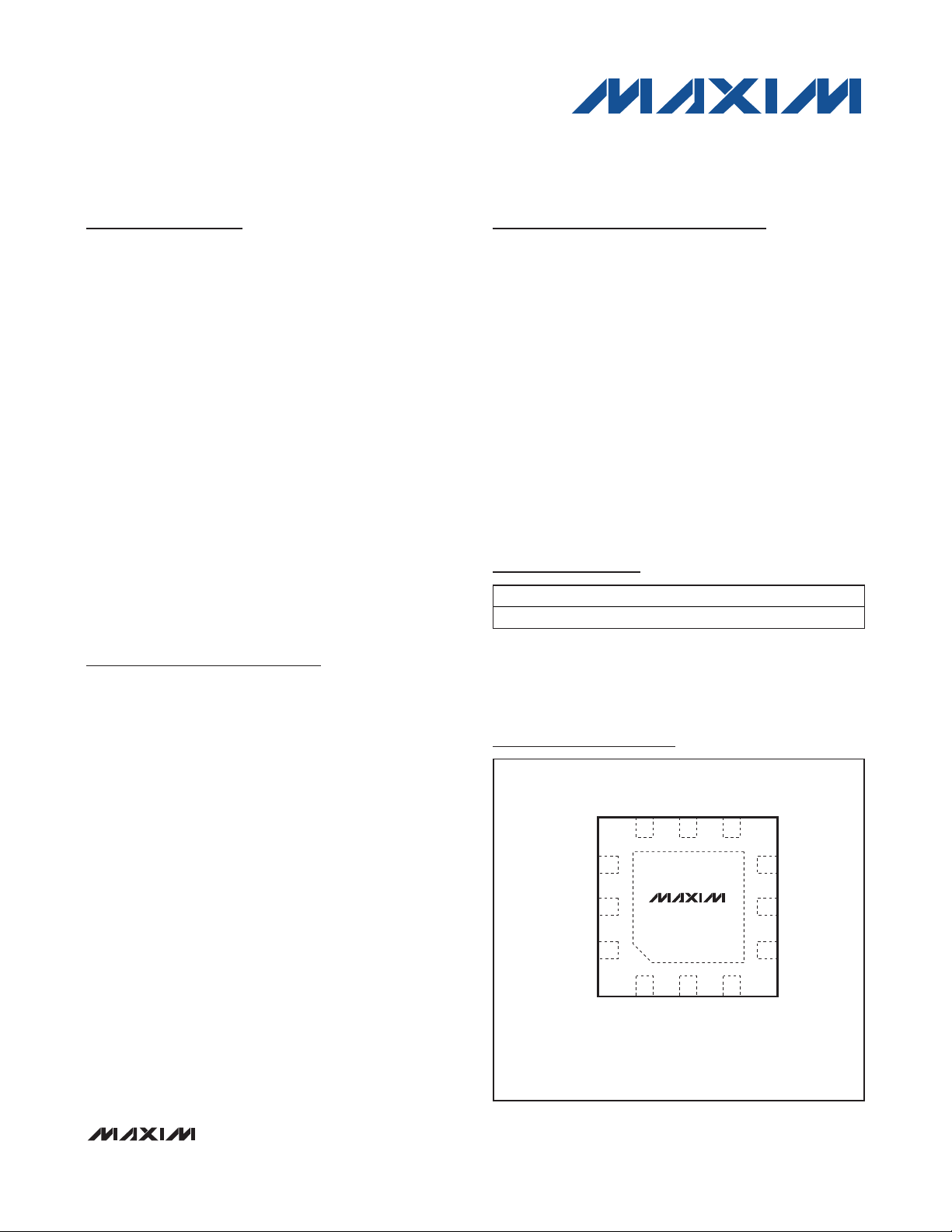
Pin Configuration
Ordering Information
*
EP = Exposed pad.
+
Denotes a lead(Pb)-free/RoHS-compliant package.
Multimedia Controls for
Multimedia-Enabled
Cell Phones
Keyboard Encoder for
Slider, Flip, and other
Cell Phones
Portable Media Players
MP3, CD, DVD Players
PDAs
Digital Still Cameras
PDA Accessory
Keyboards
Multimedia Desktop
Speakers
Portable Game
Consoles
PART TEMP RANGE PIN-PACKAGE
MAX11041ETC+ -40°C to +85°C 12 TQFN-EP*
TOP VIEW
INT
V
FORCE
SDA
987
10
11
DD
12
EXPOSED PAD CONNECTED TO GND.
MAX11041
+
12
GND
THIN QFN
(4mm x 4mm x 0.6mm)
SCL
SENSE
3
SHDN
DD
V
A0
6
5
A1
N.C.
4

MAX11041
ABSOLUTE MAXIMUM RATINGS
Stresses beyond those listed under “Absolute Maximum Ratings” may cause permanent damage to the device. These are stress ratings only, and functional
operation of the device at these or any other conditions beyond those indicated in the operational sections of the specifications is not implied. Exposure to
absolute maximum rating conditions for extended periods may affect device reliability.
VDDto GND...........................................................-0.3V to +4.0V
INT to GND.................................................-0.3V to (V
DD
+ 0.3V)
SCL, SDA, A1, A0, SHDN to GND.........................-0.3V to +4.0V
FORCE, SENSE to GND.........................................................±6V
Current into Any Pin..........................................................±50mA
Maximum ESD per IEC 61000-4-2
Human Body Model, FORCE, SENSE............................±15kV
FORCE, SENSE Short to GND....................................Continuous
Junction Temperature......................................................+150°C
Operating Temperature Range ...........................-40°C to +85°C
Storage Temperature Range .............................-65°C to +150°C
Lead Temperature (soldering, 10s) .................................+300°C
Soldering Temperature (reflow) .......................................+260°C
ELECTRICAL CHARACTERISTICS
(VDD= +1.6V to 3.6V, C
SENSE
= 10nF, R
SENSE
= 10kΩ, TA= T
MIN
to T
MAX
, unless otherwise noted. Typical values are at TA= +25°C.)
Wired Remote Controller
2 _______________________________________________________________________________________
PARAMETER SYMBOL CONDITIONS MIN TYP MAX UNITS
KEY DETECTION CHARACTERISTICS
Detectable Keys
Maximum Switch Resistance (Note 1) 100 Ω
Maximum Switch Bounce Time (Note 1) 13 ms
External Resistor Tolerance (Note 1) ±1 %
SWITCH DEBOUNCE
Debounce Analog Time Constant
Chatter Rejection Pulses shorter than this are ignored 18 ms
Rising Voltage Debounce Time t
CPW
Provided the keys meet the next three
specifications; R
recommended circuit
C
= 10nF, external resistor from
SENSE
FORCE to SENSE is 10kΩ (R
Time required for a new voltage (due to
keypress) to be detected and stored in
FIFO
connected; use
JACK
SENSE
)
30 Keys
0.4 ms
18 ms
Falling Voltage Debounce Time t
Jack Insertion Debounce Time (Note 2) 18 ms
Jack Removal Debounce Time (Note 2) 18 ms
DURATION COUNTER
Duration-Counter Resolution One tick 32 ms
Duration-Counter Range MSB is overflow bit 0 127 Counts
Duration-Counter Accuracy ±20 %
DIGITAL INPUTS (SDA, SCL, SHDN, A0, A1)
Input High Voltage V
Input Low Voltage V
Input Leakage Current IIH, I
Input Hysteresis 9%V
Input Capacitance 10 pF
LPWS
Time required for detection of key release
and final time duration to be stored in FIFO
IH
IL
IL
18 ms
0.7 x
V
DD
0.3 x
V
DD
-10 +10 µA
V
V
DD

MAX11041
Wired Remote Controller
ELECTRICAL CHARACTERISTICS (continued)
(VDD= +1.6V to 3.6V, C
SENSE
= 10nF, R
SENSE
= 10kΩ, TA= T
MIN
to T
MAX
, unless otherwise noted. Typical values are at TA= +25°C.)
____________________________________________________________________________________ 3
PARAMETER SYMBOL CONDITIONS MIN TYP MAX UNITS
DIGITAL OUTPUTS (SDA, INT)
Output High Voltage (INT)VOHI
Output Low Voltage (INT)V
Output High Leakage Current
Output Low Voltage (SDA) V
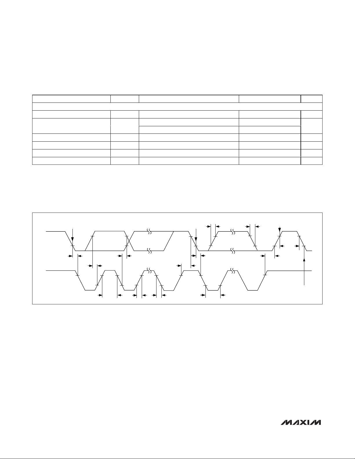
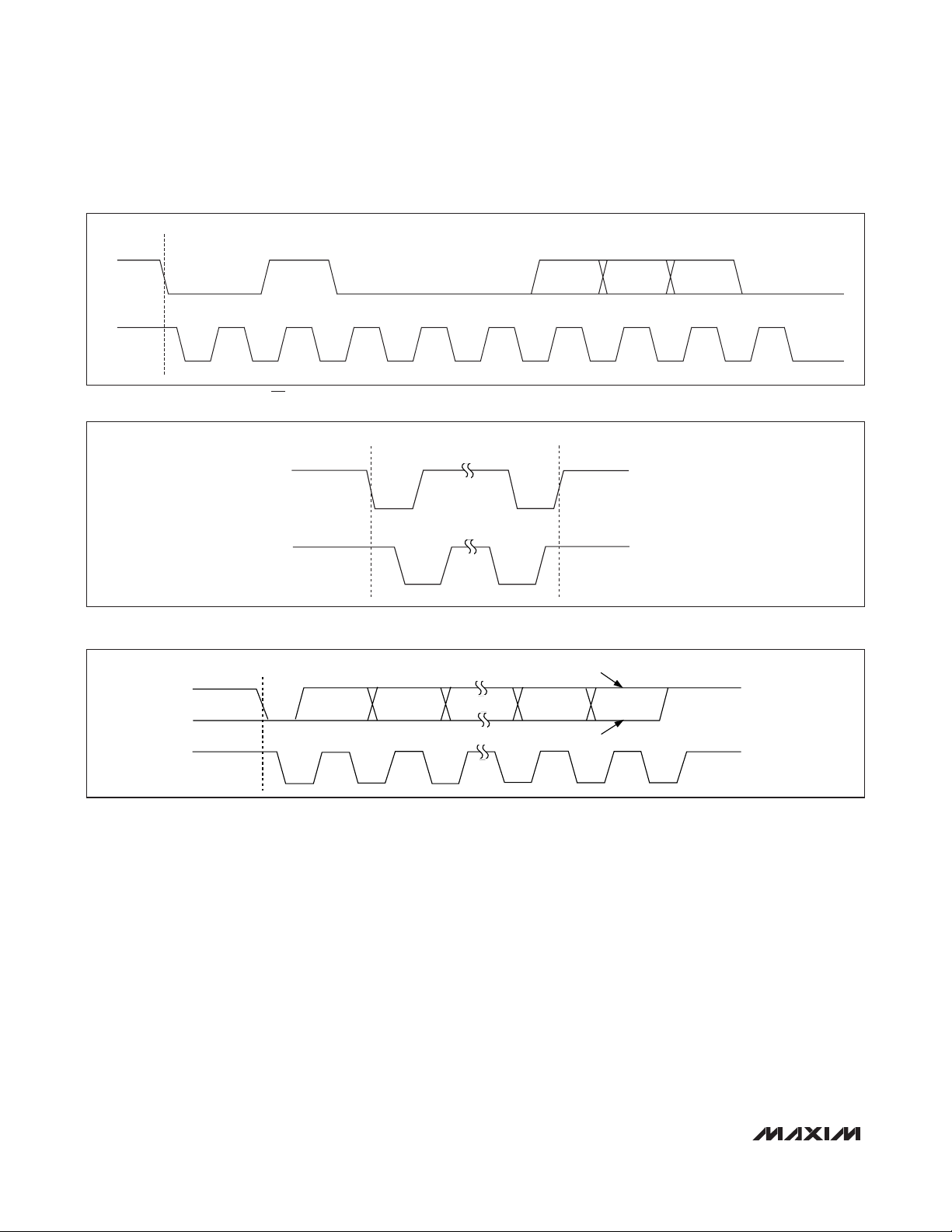
I2C TIMING CHARACTERISTICS (see Figure 1)
Serial Clock Frequency f
Bus Free Time Between STOP
and START Conditions
Hold Time (Repeated) START
Condition
SCL Pulse-Width Low t
SCL Pulse-Width High t
Setup Time for a Repeated
START Condition
Data Hold Time t
Data Setup Time t
SDA and SCL Receiving Rise
Time
SDA and SCL Receiving Fall
Time
SDA Transmitting Rise Time t
SDA Transmitting Fall Time t
Setup Time for STOP Condition t
Bus Capacitance C
Pulse Width of Suppressed Spike t
OLINTISINK
I
OHL
OLSDA
SCL
t
BUF
t
HD,STA
LOW
HIGH
t
SU,STA
HD,DAT
SU,DAT
t
RR
t
FR
RT
FT
SU,STO
b
SP
≤ 2mA
SOURCE
≤ 2mA
V
= V
OUT
DD
IOL = 3mA for VDD > 2V 0.4 V
IOL = 3mA for VDD < 2V
(Note 3)
(Note 3)
VDD = 3.6V (Note 3)
VDD = 2.4V to 3.6V
VDD = 1.6V to 2.4V
0.9 x
V
DD
0.1 x
V
DD
1µA
0.2 x
V
DD
0 400 kHz
1.3 µs
0.6 µs
1.3 µs
0.6 µs
0.6 µs
0 900 ns
100 ns
20 +
C
b
20 +
C
b
20 +
C
b
20 +
C
b
20 +
C
b
/ 10
/ 10
/ 10
/ 20
/ 20
300 ns
300 ns
250 ns
250
375
0.6 µs
400 pF
050ns
V
V
V
ns
MAX11041
Wired Remote Controller
4 _______________________________________________________________________________________
Note 1: Recommended properties of external switch for proper detection of 30 keys or key combinations.
Note 2: See the
Jack Insertion/Removal Detection
section.
Note 3: C
b
is the bus capacitance in pF.
Note 4: Key current depends on external key resistors and is calculated by V
DD
/ (30.1kΩ + RSW).
Figure 1. I2C Serial-Interface Timing
ELECTRICAL CHARACTERISTICS (continued)
(VDD= +1.6V to 3.6V, C
SENSE
= 10nF, R
SENSE
= 10kΩ, TA= T
MIN
to T
MAX
, unless otherwise noted. Typical values are at TA= +25°C.)
PARAMETER SYMBOL CONDITIONS MIN TYP MAX UNITS
POWER SUPPLIES
Power-Supply Voltage V
Average Operational Supply
Current
Shutdown Power-Supply Current I
Jack Current I
Key Current I
SHDN High to Part Active Wake-up time 5 ms
DD
I
DDOP
DDSHDN
DDJACK
DDBUTTON
1.6 3.6 V
Excluding jack/key current 5 20
Jack inserted, R
= 619kΩ 8
JACK
Excluding jack/key current 1 µA
Flowing when jack is inserted 4 µA
Flowing when keys pressed (Note 4) 90 µA
µA
START CONDITION
(S)
SDA
t
HD,STA
t
SU,DAT
SCL
t
HIGH
t
HD,DAT
REPEAT START CONDITION
(Sr)
t
SU,STA
t
RR
t
FR
t
LOW
t
HD,STA
t
RR,tRT
t
SU,STO
STOP CONDITION
t
FR,tFT
(P)
t
BUF
START CONDITION
(S)
MAX11041
Wired Remote Controller
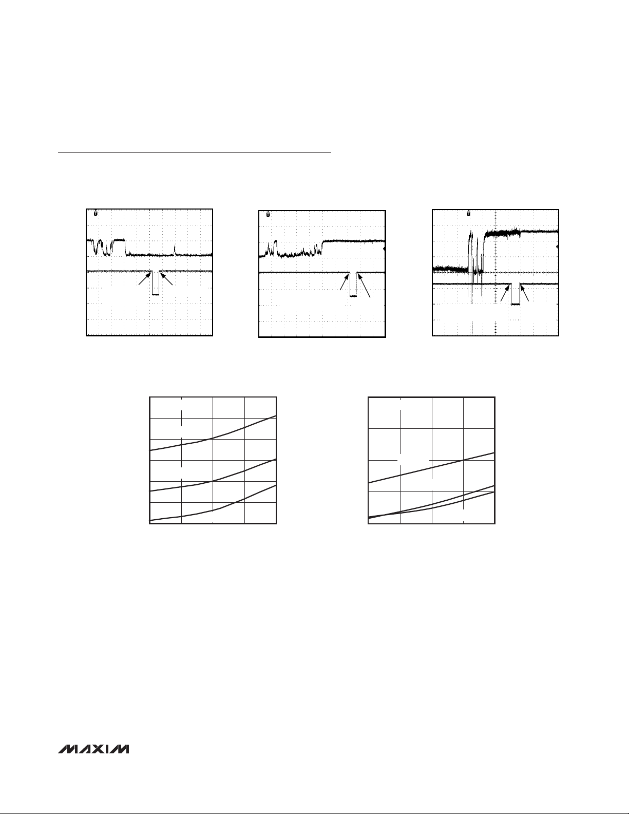
Typical Operating Characteristics
(TA = +25°C, unless otherwise noted.)
____________________________________________________________________________________ 5
*
Oscilloscope shots are taken with simulated bounce and chatter. Real switches will exhibit different bounce and chatter characteristics.
DEBOUNCE SCOPE SHOT (FALLING)
MAX11041 TOC01
V
SENSE
10ms/div
µ
P READS FIFO
INT
DEBOUNCED KEY
ADDED TO FIFO
VDD SUPPLY CURRENT vs. VOLTAGE
7.0
NO JACK INSERTED
6.5
6.0
TA = +85°C
DEBOUNCE SCOPE SHOT (RISING)
V
SENSE
INT
DEBOUNCE KEY ADDED
TO FIFO
MAX11041 TOC04
KEYPRESS RELEASE SCOPE SHOT*
MAX11041 TOC02
V
SENSE
µ
10ms/div
P READS
FIFO
VDD SHUTDOWN SUPPLY CURRENT
1.00
NO JACK INSERTED
0.75
INT
DEBOUNCE KEY ADDED
vs. VOLTAGE
TO FIFO
µ
10ms/div
MAX11041 TOC05
MAX11041 TOC03
P READS
FIFO
(µA)
5.5
DD
I
5.0
4.5
4.0
TA = +25°C
TA = -40°C
1.6 2.62.1 3.1 3.6
VDD (V)
(µA)
0.50
DD
I
0.25
0
1.6 2.62.1 3.1 3.6
TA = +85°C
TA = -40°C
TA = +25°C
VDD (V)

MAX11041
Detailed Description
The MAX11041 wired remote controller recognizes 30 different keypresses consisting of a resistor/switch array
over a single connector. Designed for wired remote controllers on the headphone or headset cord, the
MAX11041 contains debouncing circuitry and jack insertion/removal detection. During a keypress, the MAX11041
stores the key type and key duration in an 8-word FIFO
and INT (interrupt output) goes low. The results stored in
the FIFO are accessed through the I
2
C interface.
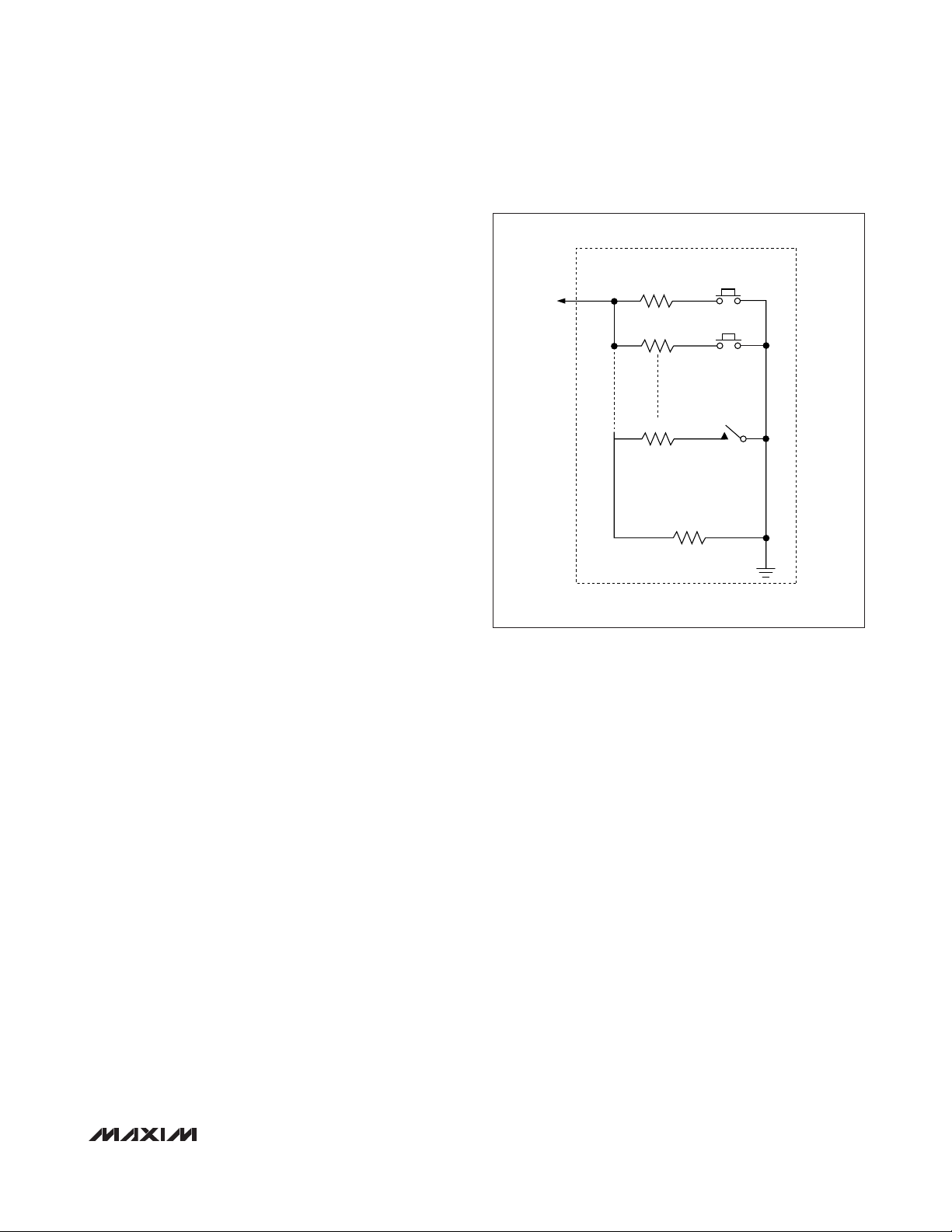
FORCE and SENSE
During a keypress, a unique external resistor (R
SW_
)
located in the remote controller connects SENSE to
ground (Figure 2). This event changes the impedance
seen by the SENSE line. The MAX11041 decodes this
resistor value to an 8-bit result (see the
Required
Resistor Set
section). FORCE and SENSE are ±15kV
ESD (IEC 61000-4-2) protected.
Register Description
The MAX11041 contains one 8-bit control register, an
8-word FIFO (each word consists of an 8-bit key value
and an 8-bit duration value), and an 8-bit chip ID.
Chip ID
The chip ID identifies the features and capabilities of the
wired remote controller to the software. For the
MAX11041, the chip ID is 0x00.
Control Register
The MAX11041 contains one control register (see Table
1). Bits C7, C6, and C5 control software shutdown. Set
FORCE high-impedance and indicate if the FIFO is
empty. Write/read to the control register through the I
2
C-
compatible serial interface (see the
Digital Serial
Interface
section).
FIFO
The MAX11041 contains an 8-word FIFO that can hold
enough information for four keypresses and releases.
Each keypress and release results in two data words
being stored into the FIFO. Each FIFO word consists of 2
bytes. The 1st byte is the decoded keypress or release
(K7–K0) and the 2nd byte is the keypress or release
duration time. Table 2 shows the format of a keypress
entry into the FIFO. Read the FIFO through the I2C-compatible serial interface (see the
Digital Serial Interface
section). At power-up, all the FIFO is reset such that
K7–K0 are set to 0xFF hex and 0x0F, and T6–T0 are set
to 0x00. See the
Applications Information
section for an
example of how data is entered into the FIFO.
Wired Remote Controller
6 _______________________________________________________________________________________
Pin Description
PIN NAME FUNCTION
1 GND Ground
Voltage Sense Input. Connect SENSE to FORCE through an external lowpass filter composed of R
2 SENSE
3, 11 V
4 N.C. No Connection. Leave unconnected or connect to VDD.
5A1I
6A0I
7 SHDN
8 SCL I2C Serial-Interface Clock Input. SCL requires a pullup resistor.
9 SDA I2C Serial-Interface Data Input/Output. SDA requires a pullup resistor.
10 INT Active-Low Interrupt Output. INT goes low when a valid keypress is detected at SENSE.
12 FORCE
EP EP Exposed Pad. Connect EP to GND.
DD
and C
SENSE.
Power-Supply Input. Connect both VDD inputs together and bypass each VDD with a 0.1µF capacitor to
GND.
2
C Address Input 1. Logic state represents bit 1 of the I2C slave address.
2
C Address Input 0. Logic state represents bit 0 of the I2C slave address.
Active-Low Shutdown Input. Bring SHDN low to put the MAX11041 in shutdown mode. FORCE is in a
high-impedance state while SHDN is low.
Force Output. Connect FORCE to the external resistor array. Connect SENSE to FORCE through an
external lowpass filter composed of R
ESD protection on FORCE.
(see the FORCE and SENSE section). There is a ±15kV IEC 61000-4-2 ESD protection on
SENSE
= 10kΩ and C
SENSE
= 10nF. There is a ±15kV IEC 61000-4-2
SENSE
SENSE

MAX11041
Wired Remote Controller
MAX11041
Figure 2. Recommended FORCE and SENSE Configuration
____________________________________________________________________________________ 7
Table 1. Control Register
Table 2. FIFO Data Format
X = Don’t care.
CIRCUIT
FORCE
SENSE
C
AUDIO
R
SENSE
SENSE
10nF
WIRED REMOTE CONTROLLER
TO
R
SW0
10kΩ
JACK/PLUG
CONNECTION
R
SW1
R
SW30
R
JACK
HOLD
SWITCH
BITS READ/WRITE POWER-UP STATE DESCRIPTION
C7 R/W 1
C6 R/W 0
C5 R 1
0 = FORCE is high-impedance
1 = FORCE is not high-impedance (normal operation)
0 = Normal operation
1 = Power-down state, full reset
1 = FIFO is empty
0 = FIFO is not empty
C4–C0 — Not used Reading/writing has no effect
FIFO DATA BIT NAMES
Keypress type (MAX11041) K7 K6 K5 K4 K3 K2 K1 K0
Keypress duration OF T6 T5 T4 T3 T2 T1 T0
MAX11041
Keypress Detection and Debounce
At power-up, the MAX11041 begins to monitor the
SENSE input for keypresses. When the MAX11041
detects a keypress at SENSE, it attempts to debounce
the SENSE input. After successful debouncing of the
input, the corresponding keypress result is inserted into
the FIFO. In addition, INT goes low to signal a keypress
to the µP.
Keypress FIFO and Time Duration
After detecting and debouncing a key, the decoded
key is stored in one byte of the 8-word FIFO. A 7-bit
internal timer starts counting the duration of the keypress (one count = 32ms) and the result is stored after
each increment in another byte of the 8-word FIFO. The
8th bit in the time duration byte is an overflow bit that
is set when the count reaches 128. After the count
reaches 128, the 7-bit timer rolls over to 0 and continues to count while the 8th bit becomes set and stays
set until the associated FIFO entry is cleared. For keypress durations longer than 8.16s, see the
Extended
Keypresses
section.
When the device detects another change in resistance
at SENSE (either by key release or another keypress),
the count resets and the FIFO begin recording the next
keypress/duration. This allows the 8-word FIFO to store
time duration and key-type information for up to four
keypresses and releases. When the FIFO is full and a
key is pressed, the oldest keypress information in the
FIFO is written over. Writing to the power-down bit (bit
6) in the control register or bringing SHDN low clears
the FIFO to its power-on-reset (POR) state.
Wired Remote Controller
8 _______________________________________________________________________________________
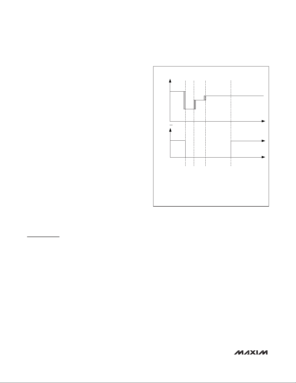
Figure 3. Reading the FIFO While the Key is Still Pressed
Figure 4. Reading the FIFO After the Key is Released
Table 3. Chip ID Data Format
CHIP ID
MAX11041 0 0000000
I7 I6 I5 I4 I3 I2 I1 I0
BIT NAMES
KEY TYPE
V
➀
➁
INT
➂
➃
TIME
KEY TYPE
V
INT
➀
➂➁
TIME
TIME
1. DEBOUNCED KEYPRESS STORED IN FIFO AND INT GOES LOW, DURATION
TIMER STARTS.
2. PROCESSOR READS FIFO AND INT GOES HIGH. KEY TYPE AND CURRENT
KEYPRESS DURATION TIME SENT. FIFO IS NOT CLEARED.
3. KEYPRESS RELEASES AND INT GOES LOW. KEY TYPE AND FINAL KEYPRESS
DURATION TIME STORED IN FIFO.
4. PROCESSOR READS THE FIFO AND INT GOES HIGH. KEYPRESS INFORMATION
STORED IN FIFO FROM STEP 3 IS CLEARED.
1. DEBOUNCED KEYPRESS STORED IN FIFO AND INT GOES LOW.
DURATION TIMER STARTS.
2. KEYPRESS RELEASES. KEY TYPE AND KEYPRESS TIME
DURATION INFORMATION STORED IN FIFO.
3. PROCESSOR READS FIFO COMPLETELY AND INT GOES HIGH.
PREVIOUS KEYPRESS INFORMATION CLEARED.
TIME

Reading the FIFO While the Key is Still Pressed
When a valid keypress occurs, INT goes low, signaling
to the processor that a key has been pressed (see
Figure 3). If the processor reads the FIFO while the key
is still pressed, the key type and current duration of the
keypress is sent. The current keypress information in
the FIFO is not cleared after a read operation if the key
is still pressed. In addition, after a read operation, if the
key is still pressed, INT goes high again until the device
detects another keypress/release, freeing the processor from polling. Conversely, if the processor chooses
to poll the duration of the keypress, INT stays high at
this time no matter how many times the processor
reads the FIFO. When INT goes low again (from another keypress/release), key type and final time duration of
the keypress is available in the FIFO. When the FIFO is
read after the key release, the information from that
keypress is cleared and INT goes high again.
Reading the FIFO After the Key has Released
When a valid keypress occurs, INT goes low, signaling
to the processor that a key has been pressed (see
Figure 4). If the processor reads the FIFO after the key
has already been released (or an additional key was
pressed), the key type and final duration time of that
keypress is sent. In addition, the information from the
keypress is cleared and INT goes high again.
Digital Serial Interface
The MAX11041 contains an I2C-compatible interface for
data communication with a host processor (SCL and
SDA). The interface supports a clock frequency up to
400kHz. SCL and SDA require pullup resistors that are
connected to a positive supply. Figure 5 details the
read and write formats.
Write Format
The only write to the MAX11041 that is possible is to the
control register (C7–C0). Use the following sequence to
write to the control register (see Figure 5):
1) After generating a START condition (S), address the
MAX11041 by sending the appropriate slave
address byte with its corresponding R/W bit set to a
0 (see the
Slave Address and
R/W
Bit
section). The
MAX11041 answers with an ACK bit (see the
Acknowledge Bits
section).
2) Send the appropriate data bytes to program the
control register (C7–C0). The MAX11041 answers
with an ACK bit.
3) Generate a STOP condition (P).
Read Format
To read the control register and key type/duration stored
in FIFO, use the following sequence (see Figure 5):
1) After generating a START condition (S), address the
MAX11041 by sending the appropriate slave
address byte with its corresponding R/W bit set to a
1 (see the
Slave Address and
R/W
Bit
section). The
MAX11041 answers with an ACK bit (see the
Acknowledge Bits
section).
2) The MAX11041 sends the 8-bit chip ID I7–I0.
Afterwards, the master must send an ACK bit.
3) The MAX11041 sends the contents of the control
register (C7–C0) starting with the most significant
bit. Afterwards, the master must send an ACK bit.
MAX11041
Wired Remote Controller
____________________________________________________________________________________ 9
WRITE FORMAT
Figure 5. Read/Write Formats
START
READ FORMAT
START
ADDRESS
BYTE 0
5 BITS 0
S PAAA1 A0
ADDRESS
BYTE 0
5 BITS A1 A0S A A A A A P
R/W
ACK STOP
ACK
R/W
1
CONTROL
REG DATA
BYTE 1
C7–C0
CHIP ID
BYTE 1
I7–I0
ACK
ACK
SLAVE TO MASTER
MASTER TO SLAVE
CONTROL
REG DATA
BYTE 2
C7–C0 K7–K0 OF, T6–T0
ACK
KEY TYPE
BYTE 3
ACK
KEY
DURATION
BYTE 4
ACK
STOP
MAX11041
4) The MAX11041 sends the latest keypress type
(K7–K0) stored in the FIFO starting with the mostsignificant bit. Afterwards the master must send an
ACK bit.
5) The MAX11041 sends the corresponding keypress
time duration (OF, T6–T0) stored in the FIFO starting with the most significant bit (OF). Afterwards the
master must send an ACK bit.
6) The master must generate a STOP condition.
Slave Address and R/WBit
The MAX11041 includes a 7-bit slave address. The first
5 bits (MSBs) of the slave address are factory-programmed and always 01000. The logic state of the
address inputs (A1 and A0) determine the last two
LSBs of the device address (see Figure 6). Connect A1
and A0 to VDD(logic high) or GND (logic low). A maximum of four MAX11041 devices can be connected on
the same bus at one time using these address inputs.
The 8th bit of the address byte is a read/write bit (R/W).
If this bit is set to 0, the device expects to receive data.
If this bit is set to 1, the device expects to send data.
Wired Remote Controller
10 ______________________________________________________________________________________
Figure 6. Slave Address and R/W Bit
Figure 7. START and STOP Conditions
Figure 8. Acknowledge Bits
S
SDA
SCL
0
12
SDA
1
S
0
3
S
SDA
SCL
0
4
0A1
5
NOT ACKNOWLEDGE
6
P
A2
78
R/W
ACK
9
ACKNOWLEDGE
SCL
1
2
8
9

MAX11041
Wired Remote Controller
___________________________________________________________________________________ 11
*
Values outside FIFO resistor code are considered invalid.
Table 4. Required Resistor Set for the MAX11041
KEY
0 0 0 1 Function 0
1 1470 11 13 Function 1
2 2550 19 21 Function 2
3 3740 27 30 Function 3
4 4990 35 38 Function 4
5 6340 42 46 Function 5
6 7680 50 53 Function 6
7 9310 58 62 Function 7
8 11000 66 70 Function 8
9 13000 74 78 Function 9
10 15000 82 86 Function 10
11 17400 90 94 Function 11
12 20000 98 102 Function 12
13 22600 105 110 Function 13
14 26100 114 119 Function 14
15 30100 123 127 Function 15
16 34000 130 135 Function 16
17 38300 137 142 Function 17
18 44200 146 150 Function 18
19 51100 154 159 Function 19
20 59000 162 166 Function 20
21 68100 170 174 Function 21
22 80600 178 182 Function 22
23 95300 186 190 Function 23
24 118000 194 198 Function 24
25 147000 202 206 Function 25
26 191000 211 214 Function 26
27 261000 218 222 Function 27
28 402000 226 229 Function 28
29 825000 235 237 Function 29
Jack inserted 619000 243 245 Jack inserted
Jack removed ∞ 254 255 Jack removed
STANDARD 1%
RESISTOR VALUE (Ω)
FIFO RESISTOR CODE*
LOWEST HIGHEST
FUNCTION
MAX11041
Bit Transfer
One data bit is transferred during each SCL clock cycle.
The data on SDA must remain stable during the high
period of the SCL clock pulse. Changes in SDA while
SCL is high and stable are considered control signals
(see the
START and STOP Conditions
section). Both
SDA and SCL remain high when the bus is not active.
START and STOP Conditions
The master initiates a transmission with a START condition, a high-to-low transition on SDA while SCL is high.
The master terminates a transmission with a STOP condition, a low-to-high transition on SDA while SCL is high
(see Figure 7).
Acknowledge Bits
Data transfers are acknowledged with an acknowledge
bit (ACK) or a not-acknowledge bit (NACK). Both the
master and the MAX11041 generates ACK bits. To generate an ACK, pull SDA low before the rising edge of
the ninth clock pulse and keep it low during the high
period of the ninth clock pulse (see Figure 8). To generate a NACK, leave SDA high before the rising edge of
the ninth clock pulse and keep it high for the duration of
the ninth clock pulse. Monitoring NACK bits allows for
detection of unsuccessful data transfers. The master
can also use NACK bits to interrupt the current data
transfer to start another data transfer. If the master uses
NACK during a read from the FIFO, the FIFO word
pointer is not incremented and the next FIFO read produces the same FIFO word. Thus, the master must provide the ACK bit to advance the FIFO word pointer.
Applications Information
Required Resistor Set
Table 4 shows the required resistor set for 30 key implementations. Resistors must have a 1% tolerance.
Jack Insertion/Removal Detection
During jack insertion there may be several
false key entries written to the FIFO. When a jack insertion/removal is detected, it is necessary to read the
FIFO repeatedly until the final change in jack state is
located (see Figure 9).
Extended Keypresses
In certain applications, a key triggers different events
depending on the duration of the keypress, simultaneous keypresses, or a specific order of keypresses.
Long Keypress Detection
In some applications, the duration of the keypress
determines the event triggered. For example, TALK
dials the entered phone number normally and initiates
voice dialing if it is held down. A second common use
of holding a key down is to generate a continuous
stream of events, such as the volume control or
fast forward.
Wired Remote Controller
12 ______________________________________________________________________________________
Figure 9. Jack Insertion Detection
KEY TYPE
JACK
REMOVED
JACK
DETECTED
FALSE
KEYS
V
INT
1. JACK INSERTION DETECTED AND ENTERED IN FIFO.
2. JACK REMOVAL DETECTED AND ENTERED IN FIFO.
3. JACK INSERTION DETECTED AND ENTERED IN FIFO.
4. FIFO IS READ UNTIL EMPTY (INT GOES HIGH).
THE LAST READ BEFORE THE EMPTY FIFO IS REACHED
IS THE FINAL STATE OF THE JACK DETECTION.
➂➁➀➃
TIME
TIME
Simultaneous Keypress Detection
Certain applications require the detection of
simultaneous keypresses, such as <SHIFT+KEY> and
<FUNCTION+KEY> combinations. This is done in
software. For instance, the µP detects the SHIFT key is
being pressed. When the µP detects an additional keypress instead of a key release, it knows the corresponding code is a result of two resistors
in parallel.
Order of Keypress Detection
Some applications require detection of the specific
sequence of keys in software by looking for unique key
presses within 32 ticks (1s). If the duration between
keypresses exceeds the allowed time, assume the keypress is in error and return to the previous known state.
Power-Up Jack Detect and Keypress
Example
Figure 10 illustrates the FIFO entries during a typical
sequence of events.
Layout, Grounding, and Bypassing
Position R
SENSE
and C
SENSE
as close to the device as
possible. Bypass VDDwith a 0.1µF capacitor to GND as
close to the device as possible. Connect GND to a
quiet analog ground plane. Route digital lines away
from SENSE and FORCE.
MAX11041
Wired Remote Controller
___________________________________________________________________________________ 13
Figure 10. Software Implemented Hold-Switch Configuration
WIRED REMOTE CONTROLLER
R
R
R
SW0
SW1
SW30
R
JACK
HOLD SWITCH
FORCE

MAX11041
Figure 10. Power-Up, Jack Detect, and Keypress Example
Wired Remote Controller
14 ______________________________________________________________________________________
V
1
SHDN TRANSITION FROM
LOW TO HIGH.
READ
POINTER
0xFF
0xFF
0xFF
0xFF
0xFF
0xFF
0xFF
0xFF
SENSE
V
INT
0x00
0x00
0x00
0x00
0x00
0x00
0x00
0x00
1
WRITE
POINTER
23
t
1t2t3
2
OPEN CIRCUIT DETECTED
READ
POINTER
45 6 7
t4 t
READ
POINTER
3
AND ENTERED IN FIFO.
DURATION
TIMER STARTS.
0xFF
TIMER...
0xFF
0x00
0x00
0xFF
0xFF
0x00
0x00
0xFF
0xFF
0x00
0x00
0xFF
0xFF
0x00
WRITE
POINTER
89
5
JACK INSERTION DETECTED AND
ENTERED IN FIFO. FINAL
DURATION TIME FROM 2
IS STORED. NEW DURATION TIME
FOR JACK DETECTION STARTS.
0xFF
/32ms
t
0xFF
0xFF
0xFF
0xFF
0xFF
0xFF
1
TIMER...
0x00
0x00
0x00
0x00
0x00
0x00
JD CODE
WRITE
POINTER
12
11
10
TIME
0xFF
0xFF
0xFF
0xFF
0xFF
0xFF
0xFF
TIME
/32ms
t
1
t2/32ms
TIMER...
0x00
0x00
0x00
0x00
0x00
WRITE
POINTER
t
6
READ
POINTER
4
JACK REMOVAL DETECTED (OPEN
CIRCUIT) AND STORED IN FIFO.
FINAL DURATION TIME FROM 3
IS STORED. NEW DURATION TIME
FOR OPEN CIRCUIT STARTS.
JD CODE
5
JACK INSERTION DETECTED AND
ENTERED IN FIFO. FINAL
DURATION TIME FROM 4
IS STORED. NEW DURATION TIME
FOR JACK DETECTION STARTS.
READ
POINTER
0xFF
JD CODE
0xFF
JD CODE
0xFF
0xFF
0xFF
0xFF
9
KEY RELEASE DETECTED (JD
CODE) AND ENTERED IN FIFO.
FINAL DURATION TIME FROM 8 IS
STORED. NEW DURATION TIME
FOR JD CODE STARTS.
0xFF
0xFF
0xFF
READ
0xFF
POINTER
KEY_ CODE
JD CODE
0xFF
0xFF
t
1
t2/32ms
t
3
TIMER...
0x00
0x00
0x00
0x00
0x00
0x00
0x00
0x00
t
/32ms
5
TIMER...
0x00
0x00
/32ms
/32ms
WRITE
POINTER
WRITE
POINTER
6
µP READS UNTIL FIFO EMPTY
FLAG IS REACHED. FURTHER
READS RESULT IN JD CODE AND
CURRENT TIME DURATION
OF JD CODE BEING SENT.
0xFF
0x00
0xFF
0x00
READ
0xFF
POINTER
JD CODE
0xFF
0xFF
0xFF
0xFF
10 11 12
µP READS UNTIL FIFO EMPTY
FLAG IS REACHED. FURTHER
READS RESULT IN JD CODE AND
CURRENT TIME DURATION
OF JD CODE BEING SENT.
0xFF
0xFF
0xFF
0xFF
READ
0xFF
POINTER
JD CODE
0xFF
0xFF
DATA ENTERED
RESET DATA (POR)
WRITE
0x00
POINTER
TIMER...
0x00
0x00
0x00
0x00
0x00
0x00
0x00
0x00
WRITE
0x00
POINTER
TIMER...
0x00
0x00
*BOTH POINTERS WRAP AROUND TO THE TOP WHEN THEY GET TO THE END OF FIFO.
7
KEY PRESS DETECTED AND
ENTERED IN FIFO. FINAL TIME
DURATION FROM 6 IS STORED.
NEW DURATION TIME FOR
KEYPRESS STARTS.
0xFF
0x00
0xFF
0xFF
0xFF
0xFF
0xFF
0xFF
0xFF
0xFF
0xFF
0xFF
0xFF
0xFF
0x00
0x00
/32ms
t
4
TIMER...
0x00
0x00
0x00
0x00
0x00
0x00
0x00
0x00
t
/32ms
6
TIMER...
0x00
READ
POINTER
JD CODE
KEY_ CODE
JACK REMOVAL DETECTED (OPEN CIRCUIT)
AND STORED IN FIFO. FINAL
DURATION TIME FROM 10
IS STORED. NEW DURATION TIME
FOR OPEN CIRCUIT STARTS.
READ
POINTER
JD CODE
WRITE
POINTER
WRITE
POINTER
8
µP READS UNTIL FIFO EMPTY
FLAG IS REACHED. FURTHER
READS RESULT IN KEY_ CODE
AND CURRENT TIME DURATION OF
KEY_ CODE BEING SENT.
0xFF
0xFF
0xFF
READ
0xFF
POINTER
KEY_ CODE
0xFF
0xFF
0xFF
µP READS UNTIL FIFO EMPTY
FLAG IS REACHED. FURTHER
READS RESULT IN 0xFF AND
CURRENT TIME DURATION
BEING SENT.
0xFF
0xFF
0xFF
0xFF
0xFF
READ
0xFF
POINTER
0xFF
0xFF
0x00
0x00
0x00
0x00
TIMER...
0x00
0x00
0x00
0x00
0x00
0x00
0x00
0x00
0x00
TIMER...
0x00
WRITE
POINTER
*
WRITE
POINTER

MAX11041
Wired Remote Controller
Functional Diagram
___________________________________________________________________________________ 15
A1
A0
SCL
SDA
INT
SHDN
V
DD
I2C
INTERFACE
GND
8-BIT
KEY
8-WORD
FIFO
8-BIT
DURATION
CONTROL
LOGIC
DURATION
TIMER
DEBOUNCE
MAX11041
FORCE
KEY
DETECTOR
±15kV ESD
SENSE

MAX11041
Wired Remote Controller
16 ______________________________________________________________________________________
Typical Operating Circuit
Chip Information
PROCESS: BiCMOS
Package Information
For the latest package outline information and land patterns, go
to www.maxim-ic.com/packages
.
PACKAGE TYPE PACKAGE CODE DOCUMENT NO.
12 TQFN-EP T1244+4
21-0139
R
SW0
R
SW1
R
SW30
2
I
S
V
BUS
µP
SCL
OUTPUT
INTERRUPT
SDA
SHDN
INT
0.01µF
2
C
I
FIFO DEBOUNCE
CONTROL
LOGIC
3.3V
DAC
DAC
3.3V
V
DD
DURATION
TIMER
AO
MAX9850
MAX11041
RESISTOR
DETECTOR
A1
HOLD
R
JACK
SWITCH
VOLUME
FORCE
SENSE
ESD
GND
10kΩ
10nF

MAX11041
Wired Remote Controller
Revision History
Maxim cannot assume responsibility for use of any circuitry other than circuitry entirely embodied in a Maxim product. No circuit patent licenses are
implied. Maxim reserves the right to change the circuitry and specifications without notice at any time.
Maxim Integrated Products, 120 San Gabriel Drive, Sunnyvale, CA 94086 408-737-7600 ____________________
17
© 2010 Maxim Integrated Products Maxim is a registered trademark of Maxim Integrated Products, Inc.
REVISION
NUMBER
1 8/07 Removed leaded package types —
2 11/08 Changed FIFO Data Format table
3 1/10 Removed the MAX11042 from the data sheet
REVISION
DATE
DESCRIPTION
PAGES
CHANGED
7
1–17
 Loading...