

Page 1
General Description
The MAX1082/MAX1083 10-bit analog-to-digital converters (ADCs) combine a 4-channel analog-input multiplexer,
high-bandwidth track/hold (T/H), and serial interface with
high conversion speed and low power consumption. The
MAX1082 operates from a single +4.5V to +5.5V supply;
the MAX1083 operates from a single +2.7V to +3.6V supply. Both devices’ analog inputs are software configurable
for unipolar/bipolar and single-ended/pseudo-differential
operation.
The 4-wire serial interface connects directly to SPI™/QSPI™
and MICROWIRE™ devices without external logic. A serial
strobe output allows direct connection to TMS320-family
digital signal processors. The MAX1082/ MAX1083 use an
external serial-interface clock to perform successiveapproximation analog-to-digital conversions. The devices
feature an internal +2.5V reference and a reference-buffer
amplifier with a ±1.5% voltage-adjustment range. An
external reference with a 1V to VDDrange may also be
used.
The MAX1082/MAX1083 provide a hard-wired SHDN pin
and four software-selectable power modes (normal operation, reduced power (REDP), fast power-down (FASTPD),
and full power-down (FULLPD)). These devices can be
programmed to shut down automatically at the end of a
conversion or to operate with reduced power. When using
the power-down modes, accessing the serial interface
automatically powers up the devices, and the quick turnon time allows them to be shut down between all conversions.
The MAX1082/MAX1083 are available in 16-pin TSSOP
packages.
Applications
Portable Data Logging
Data Acquisition
Medical Instruments
Battery-Powered Instruments
Pen Digitizers
Process Control
Features
♦ 4-Channel Single-Ended or 2-Channel
Pseudo-Differential Inputs
♦ Internal Multiplexer and Track/Hold
♦ Single-Supply Operation
+4.5V to +5.5V (MAX1082)
+2.7V to +3.6V (MAX1083)
♦ Internal +2.5V Reference
♦ 400kHz Sampling Rate (MAX1082)
♦ Low Power: 2.5mA (400ksps)
1.3mA (REDP)
0.9mA (FASTPD)
2µA (FULLPD)
♦ SPI/QSPI/MICROWIRE/TMS320-Compatible 4-Wire
Serial Interface
♦ Software-Configurable Unipolar or Bipolar Inputs
♦ 16-Pin TSSOP Package
MAX1082/MAX1083
300ksps/400ksps, Single-Supply, 4-Channel,
Serial 10-Bit ADCs with Internal Reference
________________________________________________________________ Maxim Integrated Products 1
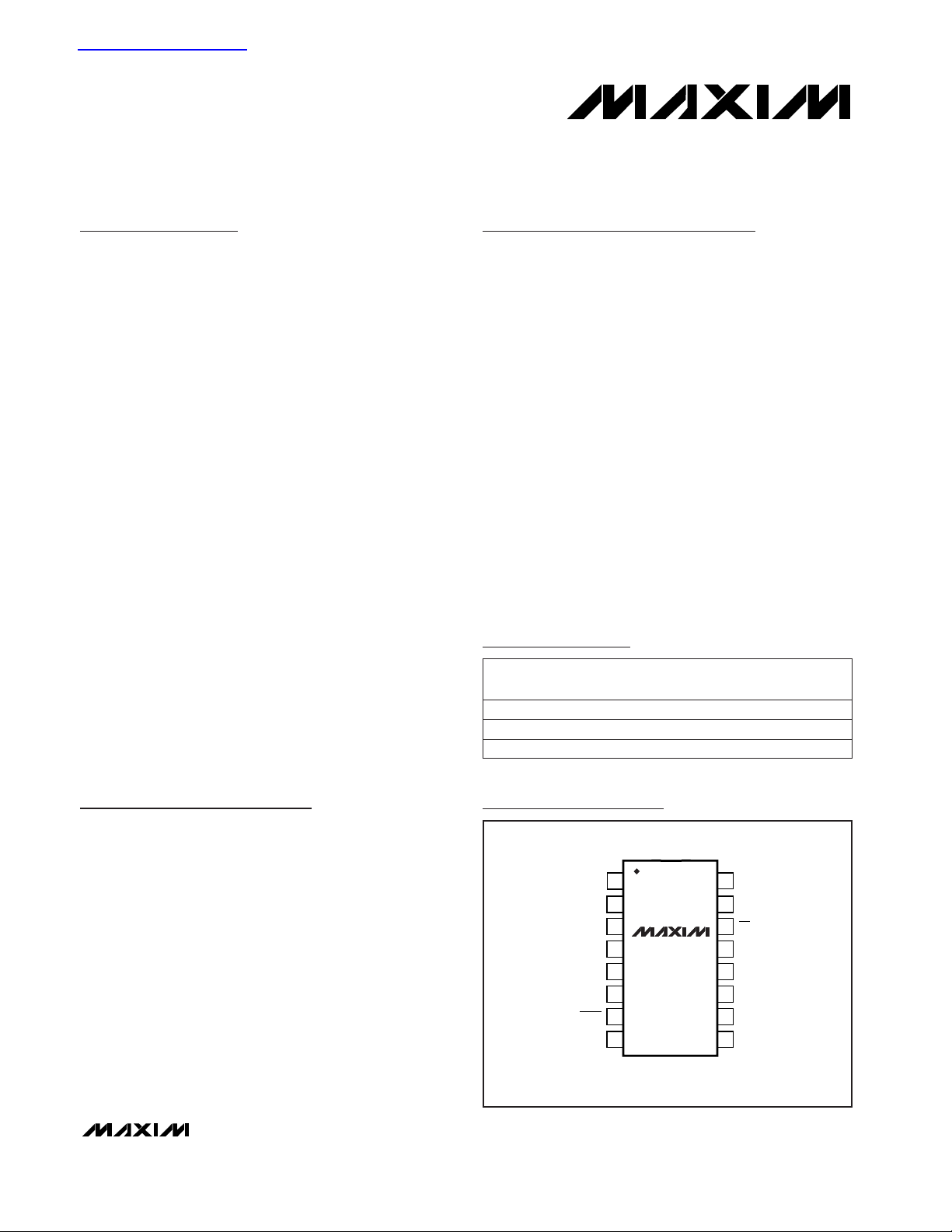
16
15
14
13
12
11
10
9
1
2
3
4
5
6
7
8
V
DD1
V
DD2
SCLK
CS
DIN
SSTRB
DOUT
GND
REFADJ
TOP VIEW
MAX1082
MAX1083
TSSOP
CH0
CH1
COM
CH2
CH3
SHDN
REF
19-1690 Rev 0; 5/00
PART
MAX1082ACUE
MAX1082BCUE
MAX1082AEUE -40°C to +85°C
0°C to +70°C
0°C to +70°C
TEMP.
RANGE
PINPACKAGE
16 TSSOP
16 TSSOP
16 TSSOP
Typical Operating Circuit appears at end of data sheet.
Pin Configuration
INL
(LSB)
±1/2
±1
±1/2
SPI and QSPI are trademarks of Motorola, Inc.
MICROWIRE is a trademark of National Semiconductor Corp.
Ordering Information continued at end of data sheet.
Ordering Information
For free samples and the latest literature, visit www.maxim-ic.com or phone 1-800-998-8800.
For small orders, phone 1-800-835-8769.
查询MAX1077供应商
Page 2
MAX1082/MAX1083
300ksps/400ksps, Single-Supply, 4-Channel,
Serial 10-Bit ADCs with Internal Reference
2 _______________________________________________________________________________________
ABSOLUTE MAXIMUM RATINGS
ELECTRICAL CHARACTERISTICS—MAX1082
(V
DD1
= V
DD2
= +4.5V to +5.5V, COM = GND, f
OSC
= 6.4MHz, 50% duty cycle, 16 clocks/conversion cycle (400ksps), external +2.5V
at REF, REFADJ = V
DD1,
TA= T
MIN
to T
MAX
, unless otherwise noted. Typical values are at TA= +25°C.)
Stresses beyond those listed under “Absolute Maximum Ratings” may cause permanent damage to the device. These are stress ratings only, and functional
operation of the device at these or any other conditions beyond those indicated in the operational sections of the specifications is not implied. Exposure to
absolute maximum rating conditions for extended periods may affect device reliability.
V
DD_
to GND............................................................ -0.3V to +6V
V
DD_
to V
DD2
....................................................... -0.3V to +0.3V
CH0–CH3, COM to GND ............................ -0.3V to (V
DD
- 0.3V)
REF, REFADJ to GND .................................. -0.3V to V
DD
- 0.3V)
Digital Inputs to GND .............................................. -0.3V to +6V
Digital Outputs to GND.............................. -0.3V to (V
DD
+ 0.3V)
Digital Output Sink Current .................................................25mA
Continuous Power Dissipation (T
A
= +70°C)
16-Pin TSSOP (derate 6.7mW/°C above +70°C) ........ 533mW
Operating Temperature Ranges
MAX1082_C_E/MAX1083_CUE ......................... 0°C to +70°C
MAX1082_E_E/MAX1083_EUE....................... -40°C to +85°C
Storage Temperature Range ............................ -60°C to +150°C
Lead Temperature (soldering, 10s) ................................ +300°C
MAX1082A
SINAD > 58dB
-3dB point
200kHz, VIN= 2.5Vp-p
f
IN1
= 99kHz, f
IN2
=102kHz
MAX1083B
No missing codes over temperature
Up to the 5th harmonic
CONDITIONS
MHz
0.5 6.4
f
SCLK
Serial Clock Frequency
ps
<50
Aperture Jitter
ns
10
Aperture Delay
ns
400
t
ACQ
Track/Hold Acquisition Time
µs
2.5
t
CONV
Conversion Time (Note 5)
kHz
350
Full-Linear Bandwidth
MHz
6
Full-Power Bandwidth
dB
-78
Channel-to-Channel Crosstalk
(Note 4)
dB
76
IMDIntermodulation Distortion
dB
70
SFDRSpurious-Free Dynamic Range
dB
-70
THDTotal Harmonic Distortion
LSB
±0.5
INLRelative Accuracy (Note 2)
bits
10
Resolution
dB
60
SINAD
Signal-to-Noise plus Distortion
Ratio
LSB
±0.2
Channel-to-Channel Offset-Error
Matching
ppm/°C
±1.6
Gain-Error Temperature
Coefficient
±1.0
LSB
±1.0
DNLDifferential Nonlinearity
LSB
±3.0
Offset Error
LSB
±3.0
Gain Error (Note 3)
UNITSMIN TYP MAXSYMBOLPARAMETER
%
40 60
Duty Cycle
DYNAMIC SPECIFICATIONS (100kHz sine-wave input, 2.5Vp-p, 400ksps, 6.4MHz clock, bipolar input mode)
DC ACCURACY (Note 1)
CONVERSION RATE
Page 3
mA
MAX1082/MAX1083
300ksps/400ksps, Single-Supply, 4-Channel,
Serial 10-Bit ADCs with Internal Reference
_______________________________________________________________________________________ 3
ELECTRICAL CHARACTERISTICS—MAX1082 (continued)
(V
DD1
= V
DD2
= +4.5V to +5.5V, COM = GND, f
OSC
= 6.4MHz, 50% duty cycle, 16 clocks/conversion cycle (400ksps), external +2.5V
at REF, REFADJ = V
DD1
, TA= T
MIN
to T
MAX
, unless otherwise noted. Typical values are at TA= +25°C.)
CONDITIONS UNITSMIN TYP MAXSYMBOLPARAMETER
To power down the internal reference
For small adjustments, from 1.22V
0 to 1mA output load
On/off leakage current, V
COM VCH_
= 0 or V
DD1
TA= +25°C
Bipolar, V
COM
or V
CH_
= V
REF
/2, referenced
to COM or CH_
Unipolar, V
COM
= 0
V/V
+2.05
Buffer Voltage Gain
V
1.4 V
DD1
- 1.0
REFADJ Buffer Disable
Threshold
mV
±100
REFADJ Input Range
V
1.22
REFADJ Output Voltage
µF
0.01 10
Capacitive Bypass at REFADJ
µF
4.7 10
Capacitive Bypass at REF
mV/mA
0.05 2.0
Load Regulation (Note 7)
ppm/°C
±15
TC V
REF
REF Output Temperature
Coefficient
mA
15
REF Short-Circuit Current
V
2.480 2.500 2.520
V
REF
REF Output Voltage
pF18Input Capacitance
µA
±0.001 ±1
Multiplexer Leakage Current
±V
REF
/2
V
V
REF
V
CH_
Input Voltage Range, Single
Ended and Differential (Note 6)
VIN= 0 or V
DD2
In full power-down mode, f
SCLK
= 0
V
REF
= 2.500V, f
SCLK
= 0
V
REF
= 2.500V, f
SCLK
= f
MAX
(Note 8)
pFC
IN
Input Capacitance
µA±1I
IN
Input Leakage
V0.2V
HYST
Input Hysteresis
V0.8V
INL
Input Low Voltage
V3.0V
INH
Input High Voltage
5
320
µA
200 350
REF Input Current
V
1.0 V
DD1
+
50mV
REF Input Voltage Range
I
SINK
= 5mA V0.4V
OL
Output Voltage Low
15
I
SOURCE
= 1mA V4V
OH
Output Voltage High
CS = V
DD2
µA±10I
L
Three-State Leakage Current
CS = V
DD2
pF15C
OUT
Three-State Output Capacitance
ANALOG INPUTS (CH3–CH0, COM)
EXTERNAL REFERENCE (reference buffer disabled, reference applied to REF)
INTERNAL REFERENCE
DIGITAL INPUTS (DIN, SCLK, CS, SHDN)
DIGITAL OUTPUTS (DOUT, SSTRB)
Page 4
MAX1082/MAX1083
300ksps/400ksps, Single-Supply, 4-Channel,
Serial 10-Bit ADCs with Internal Reference
4 _______________________________________________________________________________________
V
DD1
=
V
DD2
=
5.5V
V
DD1
= V
DD2
= 5V ±10%, midscale input
CONDITIONS
mA
2.5 4.0
IV
DD1
+ IV
DD2
Supply Current
V4.5 5.5
V
DD1,
V
DD2
Positive Supply Voltage
(Note 9)
1.3 2.0
0.9 1.5
µA
2.0 10
mV±0.5 ±2.0PSRPower-Supply Rejection
UNITSMIN TYP MAXSYMBOLPARAMETER
Normal operating mode (Note 10)
Reduced-power mode (Note 11)
Fast power-down mode (Note 11)
Full power-down mode (Note 11)
ELECTRICAL CHARACTERISTICS—MAX1082 (continued)
(V
DD1
= V
DD2
= +4.5V to +5.5V, COM = GND, f
OSC
= 6.4MHz, 50% duty cycle, 16 clocks/conversion cycle (400ksps), external +2.5V
at REF, REFADJ = V
DD1
, TA= T
MIN
to T
MAX
, unless otherwise noted. Typical values are at TA= +25°C.)
ELECTRICAL CHARACTERISTICS—MAX1083
(V
DD1
= V
DD2
= +2.7V to +3.6V, COM = GND, f
OSC
= 4.8MHz, 50% duty cycle, 16 clocks/conversion cycle (300ksps), external
+2.5V at REF, REFADJ = V
DD1
, TA= T
MIN
to T
MAX
, unless otherwise noted. Typical values are at TA= +25°C.)
MAX1083A
SINAD > 58dB
-3dB point
f = 150kHz, VIN= 2.5Vp-p
f
IN1
= 73kHz, f
IN2
=77kHz
MAX1083B
No missing codes over temperature
Up to the 5th harmonic
CONDITIONS
kHz
250
Full-Linear Bandwidth
MHz
3
Full-Power Bandwidth
dB
-78
Channel-to-Channel Crosstalk
(Note 4)
dB
76
IMDIntermodulation Distortion
dB
70
SFDRSpurious-Free Dynamic Range
dB
-70
THDTotal Harmonic Distortion
LSB
±0.5
INLRelative Accuracy (Note 2)
bits
10
Resolution
dB
60
SINAD
Signal-to-Noise plus Distortion
Ratio
LSB
±0.2
Channel-to-Channel Offset-Error
Matching
ppm/°C
±1.6
Gain-Error Temperature
Coefficient
±1.0
LSB
±1.0
DNLDifferential Nonlinearity
LSB
±3.0
Offset Error
LSB
±3.0
Gain Error (Note 3)
UNITSMIN TYP MAXSYMBOLPARAMETER
POWER SUPPLY
DC ACCURACY (Note 1)
DYNAMIC SPECIFICATIONS (75kHz sine wave input, 2.5Vp-p, 300 ksps, 4.8 MHz clock, bipolar input mode)
Page 5
MAX1082/MAX1083
300ksps/400ksps, Single-Supply, 4-Channel,
Serial 10-Bit ADCs with Internal Reference
_______________________________________________________________________________________ 5
ELECTRICAL CHARACTERISTICS—MAX1083 (continued)
(V
DD1
= V
DD2
= +2.7V to +3.6V, COM = GND, f
OSC
= 4.8MHz, 50% duty cycle, 16 clocks/conversion cycle (300ksps), external
+2.5V at REF, REFADJ = V
DD1
, TA= T
MIN
to T
MAX
, unless otherwise noted. Typical values are at TA= +25°C.)
Normal operating mode
Normal operating mode
Normal operating mode
CONDITIONS
MHz
0.5 4.8
f
SCLK
Serial Clock Frequency
ps
<50
Aperture Jitter
ns
10
Aperture Delay
ns
625
t
ACQ
Track/Hold Acquisition Time
µs
3.3
t
CONV
Conversion Time (Note 5)
UNITSMIN TYP MAXSYMBOLPARAMETER
To power down the internal reference
For small adjustments, from 1.22V
0 to 0.75mA output load
On/off leakage current, V
CH_
= 0 or V
DD1
TA= +25°C
Bipolar, V
COM
or V
CH_
= V
REF
/2,
referenced to COM or CH_
Unipolar, V
COM
= 0
V/V
2.05
Buffer Voltage Gain
V
1.4 V
DD1
- 1
REFADJ Buffer Disable
Threshold
mV
±100
REFADJ Input Range
V
1.22
REFADJ Output Voltage
µF
0.01 10
Capacitive Bypass at REFADJ
µF
4.7 10
Capacitive Bypass at REF
mV/mA
0.1 2.0
Load Regulation (Note 7)
ppm/°C
±15
TC V
REF
REF Output Temperature
Coefficient
mA
15
REF Short-Circuit Current
V
2.480 2.500 2.520
V
REF
REF Output Voltage
pF18Input Capacitance
µA
±0.001 ±1
Multiplexer Leakage Current
±V
REF
/2
%
40 60
Duty Cycle
V
V
REF
V
CH_
Input Voltage Range, Single
Ended and Differential (Note 6)
VIN= 0 or V
DD2
In full power-down mode, f
SCLK
= 0
V
REF
= 2.500V, f
SCLK
= 0
V
REF
= 2.500V, f
SCLK
= f
MAX
(Note 8)
pF
15
C
IN
Input Capacitance
µA
±1
I
IN
Input Leakage
V
0.2
V
HYST
Input Hysteresis
V
0.8
V
INL
Input Low Voltage
V
2.0
V
INH
Input High Voltage
5
REF Input Current
320
µA
200 350
V
1.0 V
DD1
+
50mV
REF Input Voltage Range
V/V
+2.05
Buffer Voltage Gain
CONVERSION RATE
ANALOG INPUTS (CH3–CH0, COM)
INTERNAL REFERENCE
EXTERNAL REFERENCE (reference buffer disabled, reference applied to REF)
DIGITAL INPUTS (DIN, SCLK, CS, SHDN)
Page 6
MAX1082/MAX1083
300ksps/400ksps, Single-Supply, 4-Channel,
Serial 10-Bit ADCs with Internal Reference
6 _______________________________________________________________________________________
V
DD1
=
V
DD2
=
3.6V
I
SOURCE
= 0.5mA
V
DD1
= V
DD2
= 2.7V to 3.6V, midscale input
CONDITIONS
mA
2.5 3.5
IV
DD1
+ IV
DD2
Supply Current
V2.7 3.6
V
DD1,
V
DD2
VV
DD2
- 0.5VV
OH
Output Voltage High
Positive Supply Voltage
(Note 9)
1.3 2.0
Normal operating mode (Note 10)
Reduced-power mode (Note 11)
0.9 1.5
Fast power-down mode (Note 11)
Full power-down mode (Note 11) µA
2.0 1.0
mV±0.5 ±2.0PSRPower-Supply Rejection
UNITSMIN TYP MAXSYMBOLPARAMETER
I
SINK
= 5mA V0.4V
OL
Output Voltage Low
CS = V
DD2
µA±10I
L
Three-State Leakage Current
CS = V
DD2
pF15C
OUT
Three-State Output Capacitance
ELECTRICAL CHARACTERISTICS—MAX1083 (continued)
(V
DD1
= V
DD2
= +2.7V to +3.6V, COM = GND, f
OSC
= 4.8MHz, 50% duty cycle, 16 clocks/conversion cycle (300ksps), external
+2.5V at REF, REFADJ = V
DD1
, TA= T
MIN
to T
MAX
, unless otherwise noted. Typical values are at TA= +25°C.)
TIMING CHARACTERISTICS—MAX1082
(Figures 1, 2, 5, 6; V
DD1
= V
DD2
= +4.5V to +5.5V; TA= T
MIN
to T
MAX
; unless otherwise noted.)
C
LOAD
= 20pF
C
LOAD
= 20pF
C
LOAD
= 20pF
C
LOAD
= 20pF
C
LOAD
= 20pF
C
LOAD
= 20pF
C
LOAD
= 20pF
C
LOAD
= 20pF
CONDITIONS
ns
100
t
CSW
CS Pulse Width High
ns
65
t
STE
CS Fall to SSTRB Enable
ns
65
t
DOE
CS Fall to DOUT Enable
ns
10 65
t
STD
CS Rise to SSTRB Disable
ns
10 65
t
DOD
CS Rise to DOUT Disable
ns
80
t
STV
SCLK Rise to SSTRB Valid
ns
80
t
DOV
SCLK Rise to DOUT Valid
ns
62
t
CL
SCLK Pulse Width Low
ns
62
t
CH
ns
156
t
CP
SCLK Period
SCLK Pulse Width High
ns
10 20
t
STH
SCLK Rise to SSTRB Hold
ns
10 20
t
DOH
SCLK Rise to DOUT Hold
ns
35
t
CS1
CS Rise to SCLK Rise Ignore
ns
35
t
CSO
SCLK Rise to CS Fall Ignore
ns
35
t
DS
DIN to SCLK Setup
ns
0
t
DH
DIN to SCLK Hold
ns
35
t
CSS
CS Fall to SCLK Rise Setup
ns
0
t
CSH
SCLK Rise to CS Rise Hold
UNITSMIN TYP MAXSYMBOLPARAMETER
DIGITAL OUTPUTS (DOUT, SSTRB)
POWER SUPPLY
Page 7
MAX1082/MAX1083
300ksps/400ksps, Single-Supply, 4-Channel,
Serial 10-Bit ADCs with Internal Reference
_______________________________________________________________________________________ 7
TIMING CHARACTERISTICS—MAX1083
(Figures 1, 2, 5, 6; V
DD1
= V
DD2
= +2.7V to +3.6V; TA= T
MIN
to T
MAX
; unless otherwise noted.)
C
LOAD
= 20pF
C
LOAD
= 20pF
C
LOAD
= 20pF
C
LOAD
= 20pF
C
LOAD
= 20pF
C
LOAD
= 20pF
C
LOAD
= 20pF
C
LOAD
= 20pF
CONDITIONS
ns
100
t
CSW
CS Pulse Width High
ns
85
t
STE
CS Fall to SSTRB Enable
ns
85
t
DOE
CS Fall to DOUT Enable
ns
13 85
t
STD
CS Rise to SSTRB Disable
ns
13 85
t
DOD
CS Rise to DOUT Disable
ns
100
t
STV
SCLK Rise to SSTRB Valid
ns
100
t
DOV
SCLK Rise to DOUT Valid
ns
83
t
CL
SCLK Pulse Width Low
ns
83
t
CH
ns
208
t
CP
SCLK Period
SCLK Pulse Width High
ns
13 20
t
STH
SCLK Rise to SSTRB Hold
ns
13 20
t
DOH
SCLK Rise to DOUT Hold
ns
45
t
CS1
CS Rise to SCLK Rise Ignore
ns
45
t
CSO
SCLK Rise to CS Fall ignore
ns
45
t
DS
DIN to SCLK Setup
ns
0
t
DH
DIN to SCLK Hold
ns
45
t
CSS
CS Fall to SCLK Rise Setup
ns
0
t
CSH
SCLK Rise to CS Rise Hold
UNITSMIN TYP MAXSYMBOLPARAMETER
Note 1: Tested at V
DD1
= V
DD2
= V
DD(MIN)
; COM = GND, unipolar single-ended input mode.
Note 2: Relative accuracy is the deviation of the analog value at any code from its theoretical value after the full-scale range has
been calibrated.
Note 3: Offset nulled.
Note 4: Ground the “on” channel; sine wave is applied to all “off” channels.
Note 5: Conversion time is defined as the number of clock cycles multiplied by the clock period; clock has 50% duty cycle.
Note 6: The common-mode range for the analog inputs (CH3–CH0 and COM) is from GND to V
DD1
.
Note 7: External load should not change during conversion for specified accuracy.
Note 8: ADC performance is limited by the converter’s noise floor, typically 300µVp-p. An external reference below 2.5V
compromises the performance of the ADC.
Note 9: Electrical characteristics are guaranteed from V
DD1(MIN)
= V
DD2(MIN)
to V
DD1(MAX)
= V
DD2(MAX)
. For operations beyond
this range, see Typical Operating Characteristics. For guaranteed specifications beyond the limits, contact the factory.
Note 10: AIN = midscale.Unipolar Mode. MAX1082 tested with 20pF on DOUT, 20pF on SSTRB, and f
SCLK
= 6.4MHz, 0 to 5V.
MAX1083 tested with same loads, f
SCLK
= 4.8MHz, 0 to 3V.
Note 11: SCLK = DIN = GND. CS = V
DD1.
Page 8
MAX1082/MAX1083
300ksps/400ksps, Single-Supply, 4-Channel,
Serial 10-Bit ADCs with Internal Reference
8 _______________________________________________________________________________________
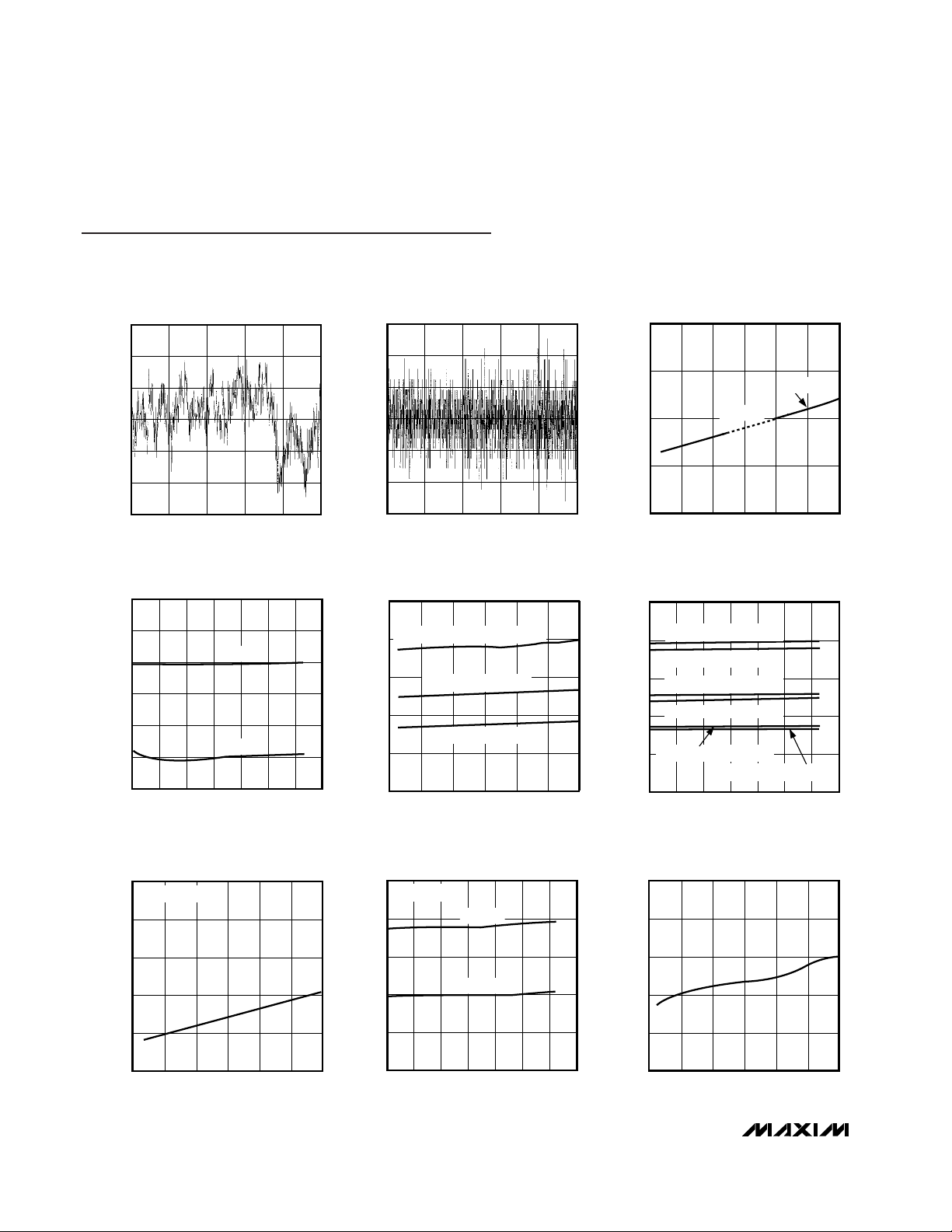
Typical Operating Characteristics
(MAX1082: V
DD1
= V
DD2
= 5.0V, f
SCLK
= 6.4MHz; MAX1083: V
DD1
= V
DD2
= 3.0V, f
SCLK
= 4.8MHz; C
LOAD
= 20pF, 4.7µF capacitor
at REF, 0.01µF capacitor at REFADJ, TA= +25°C, unless otherwise noted.)
-0.10
0
-0.05
0.10
0.05
0.15
0.20
0 400200 600 800 1000
INTEGRAL NONLINEARITY
vs. DIGITAL OUTPUT CODE
MAX1080/1-01
DIGITAL OUTPUT CODE
DNL (LSB)
-0.15
-0.05
-0.10
0.05
0
0.10
0.15
0 400200 600 800 1000
DIFFERENTIAL NONLINEARITY
vs. DIGITAL OUTPUT CODE
MAX1080/1-02
DIGITAL OUTPUT CODE
DNL (LSB)
3.5
3.0
2.5
2.0
1.5
2.5 4.03.0 3.5 4.5 5.0 5.5
SUPPLY CURRENT vs. SUPPLY
VOLTAGE (CONVERTING)
MAX1080/1-03
SUPPLY VOLTAGE (V)
SUPPLY CURRENT (mA)
MAX1083
MAX1082
2.0
2.4
2.2
2.8
2.6
3.0
3.2
-40 20 40-20 0 60 80 100
SUPPLY CURRENT vs. TEMPERATURE
MAX1080/1-04
TEMPERATURE (°C)
SUPPLY CURRENT (mA)
MAX1083
MAX1082
NORMAL OPERATION (PD1 = PD0 = 1)
REDP (PD1 = 1, PD0 = 0)
FASTPD (PD1 = 0, PD0 = 1)
0
0.5
1.5
1.0
2.0
2.5
2.5 3.53.0 4.0 4.5 5.0 5.5
SUPPLY CURRENT vs. SUPPLY
VOLTAGE (STATIC)
MAX1080/1-05
SUPPLY VOLTAGE (V)
SUPPLY CURRENT (mA)
0
0.5
1.5
1.0
2.0
2.5
-40 0-20 20 40 60 80 100
SUPPLY CURRENT vs. TEMPERATURE
(STATIC)
MAX1080/1-06
TEMPERATURE (°C)
SUPPLY CURRENT (mA)
MAX1082 (PD1 = 1, PD0 = 1)
MAX1082 (PD1 = 1, PD0 = 0)
MAX1082 (PD1 = 0, PD0 = 1)
MAX1083 (PD1 = 1, PD0 = 1)
MAX1083 (PD1 = 1, PD0 = 0)
MAX1083 (PD1 = 0, PD0 = 1)
0
1
3
2
4
5
2.5 3.53.0 4.0 4.5 5.0 5.5
SHUTDOWN SUPPLY CURRENT
vs. SUPPLY VOLTAGE
MAX1080/1-07
SUPPLY VOLTAGE (V)
SUPPLY CURRENT (µA)
(PD1 = PD0 = 0)
0
0.5
1.5
1.0
2.0
2.5
-40 0-20 20 40 60 80 100
SHUTDOWN SUPPLY CURRENT
vs. TEMPERATURE
MAX1080/1-08
TEMPERATURE (°C)
SUPPLY CURRENT (µA)
MAX1083
MAX1082
(PD1 = PD0 = 0)
2.4995
2.4997
2.5001
2.4999
2.5003
2.5005
2.5 3.53.0 4.0 4.5 5.0 5.5
REFERENCE VOLTAGE
vs. SUPPLY VOLTAGE
MAX1080/1-09
SUPPLY VOLTAGE (V)
REFERENCE VOLTAGE (V)
Page 9
MAX1082/MAX1083
300ksps/400ksps, Single-Supply, 4-Channel,
Serial 10-Bit ADCs with Internal Reference
_______________________________________________________________________________________ 9
2.4988
2.4992
2.4990
2.4996
2.4994
2.5000
2.4998
2.5002
-40 0 20-20 40 60 80 100
REFERENCE VOLTAGE
vs. TEMPERATURE
MAX1080/1-10
TEMPERATURE (°C)
REFERENCE VOLTAGE (V)
MAX1083
MAX1082
-0.50
-0.25
0
0.25
0.50
2.5 3.53.0 4.0 4.5 5.0 5.5
OFFSET ERROR vs. SUPPLY VOLTAGE
MAX1082/3-11
SUPPLY VOLTAGE (V)
OFFSET ERROR (LSB)
-0.50
-0.25
0
-40 10-15 35 60 85
OFFSET ERROR vs. TEMPERATURE
MAX1080/1-12
TEMPERATURE (°C)
OFFSET ERROR (LSB)
-0.25
-0.10
-0.15
-0.20
-0.05
0
0.05
0.10
0.15
0.20
0.25
2.5 3.53.0 4.0 4.5 5.0 5.5
GAIN ERROR vs. SUPPLY VOLTAGE
MAX1082/3-13
SUPPLY VOLTAGE (V)
GAIN ERROR (LSB)
-.50
-.25
0
GAIN ERROR vs. TEMPERATURE
MAX1080/1-14
TEMPERATURE (°C)
GAIN ERROR (LSB)
-40 10-15 35 60 85
Typical Operating Characteristics (continued)
(MAX1082: V
DD1
= V
DD2
= 5.0V, f
SCLK
= 6.4MHz; MAX1083: V
DD1
= V
DD2
= 3.0V, f
SCLK
= 4.8MHz; C
LOAD
= 20pF, 4.7µF capacitor
at REF, 0.01µF capacitor at REFADJ, TA= +25°C, unless otherwise noted.)
Page 10

MAX1082/MAX1083
300ksps/400ksps, Single-Supply, 4-Channel,
Serial 10-Bit ADCs with Internal Reference
10 ______________________________________________________________________________________
Pin Description
Positive Supply VoltageV
DD2
16
Input to the Reference-Buffer Amplifier. To disable the reference-buffer amplifier, connect REFADJ to V
DD1
.REFADJ9
Serial Strobe Output. SSTRB pulses high for one clock period before the MSB decision. High impedance when CS is high.
SSTRB12
Serial-Data Input. Data is clocked in at SCLK’s rising edge.DIN13
Active-Low Chip Select. Data will not be clocked into DIN unless CS is low. When CS is high, DOUT
and SSTRB are high impedance.
CS
14
Serial-Clock Input. Clocks data in and out of serial interface and sets the conversion speed. (Duty
cycle must be 40% to 60%.)
SCLK15
Reference-Buffer Output/ADC Reference Input. Reference voltage for analog-to-digital conversion.
In internal reference mode, the reference buffer provides a 2.500V nominal output, externally
adjustable at REFADJ. In external reference mode, disable the internal buffer by pulling REFADJ to
V
DD1
.
REF8
GroundGND10
Serial-Data Output. Data is clocked out at SCLK’s rising edge. High impedance when CS is high.
DOUT11
Active-Low Shutdown Input. Pulling SHDN low shuts down the device, reducing supply current to 2µA
(typ).
SHDN
7
Ground Reference for Analog Inputs. COM sets zero-code voltage in single-ended mode. Must be
stable to ±0.5LSB.
COM6
PIN
Positive Supply VoltageV
DD1
1
FUNCTIONNAME
Figure 1. Load Circuits for Enable Time
Figure 2. Load Circuits for Disable Time
Sampling Analog InputsCH0–CH32–5
GND
and VOL to V
V
DD2
DOUT
C
LOAD
20pF
OH
b) High-Z to VOL and VOH to V
3k
C
20pF
GND
LOAD
OL
DOUT
C
3k
GND
a) V
to High-Z b) VOL to High-Z
OH
LOAD
20pF
DOUT
3k
a) High-Z to V
OH
DOUT
V
DD2
3k
C
LOAD
20pF
GND
Page 11

Detailed Description
The MAX1082/MAX1083 ADCs use a successiveapproximation conversion technique and input T/H circuitry to convert an analog signal to a 10-bit digital output. A flexible serial interface provides easy interface to
microprocessors (µPs). Figure 3 shows a functional diagram of the MAX1082/MAX1083.
Pseudo-Differential Input
The equivalent circuit of Figure 4 shows the MAX1082/
MAX1083’s input architecture, which is composed of a
T/H, input multiplexer, input comparator, switchedcapacitor DAC, and reference.
In single-ended mode, the positive input (IN+) is connected to the selected input channel and the negative
input (IN-) is set to COM. In differential mode, IN+ and
IN- are selected from the following pairs: CH0/CH1 and
CH2/CH3. Configure the channels according to Tables
1 and 2.
The MAX1082/MAX1083 input configuration is pseudodifferential because only the signal at IN+ is sampled.
The return side (IN-) is connected to the sampling
capacitor while converting and must remain stable
within ±0.5LSB (±0.1LSB for best results) with respect
to GND during a conversion.
If a varying signal is applied to the selected IN-, its
amplitude and frequency must be limited to maintain
accuracy. The following equations express the relationship between the maximum signal amplitude and its
frequency to maintain ±0.5LSB accuracy. Assuming a
sinusoidal signal at IN-, the input voltage is determined
by:
The maximum voltage variation is determined by:
A 2.6Vp-p, 60Hz signal at IN- will generate a ±0.5LSB
error when using a +2.5V reference voltage and a
2.5µs conversion time (15 / f
SCLK
). When a DC reference voltage is used at IN-, connect a 0.1µF capacitor
to GND to minimize noise at the input.
During the acquisition interval, the channel selected as
the positive input (IN+) charges capacitor C
HOLD
. The
acquisition interval spans three SCLK cycles and ends
on the falling SCLK edge after the input control word’s
last bit has been entered. At the end of the acquisition
interval, the T/H switch opens, retaining charge on
C
HOLD
as a sample of the signal at IN+. The conversion interval begins with the input multiplexer switching
C
HOLD
from IN+ to IN-. This unbalances node ZERO at
the comparator’s input. The capacitive DAC adjusts
during the remainder of the conversion cycle to restore
node ZERO to V
DD1
/2 within the limits of 10-bit resolution. This action is equivalent to transferring a
12pF x (VIN+ - VIN-) charge from C
HOLD
to the binaryweighted capacitive DAC, which in turn forms a digital
representation of the analog input signal.
max
()
d
dt
Vf
LSB
t
V
t
V
IN
CONV
REF
CONV
IN
−
=−≤ =2
1
2
10
π
VV ft
IN IN
−= −( )sin( )2π
MAX1082/MAX1083
300ksps/400ksps, Single-Supply, 4-Channel,
Serial 10-Bit ADCs with Internal Reference
______________________________________________________________________________________ 11
INPUT
SHIFT
REGISTER
CONTROL
LOGIC
INT
CLOCK
OUTPUT
SHIFT
REGISTER
+1.22V
REFERENCE
T/H
ANALOG
INPUT
MUX
10 + 2-BIT
SAR ADC
IN
DOUT
SSTRB
V
DD1
V
DD2
GND
SCLK
DIN
COM
REFADJ
REF
OUT
REF
CLOCK
+2.500V
17k
7
8
9
6
11
12
13
14
15
CH1
3
CH2
4
CH3
5
CH0
2
MAX1282
MAX1283
CS
SHDN
1
16
10
2.05
A
≈
Figure 3. Functional Diagram
C
HOLD
12pF
R
IN
800Ω
HOLD
INPUT
MUX
C
SWITCH
*
*INCLUDES ALL INPUT PARASITICS
SINGLE-ENDED MODE: IN+ = CH0–CH3, IN- = COM.
PSEUDO-DIFFERENTIAL MODE: IN+ AND IN- SELECTED FROM
PAIRS OF CH0/CH1 AND CH2/CH3.
AT THE SAMPLING INSTANT,
THE MUX INPUT SWITCHES FROM
THE SELECTED IN+ CHANNEL TO
THE SELECTED IN- CHANNEL.
CH0
REF
GND
CH1
CH2
CH3
COM
ZERO
V
DD1
/2
COMPARATOR
CAPACITIVE
DAC
6pF
TRACK
Figure 4. Equivalent Input Circuit
Page 12

MAX1082/MAX1083
300ksps/400ksps, Single-Supply, 4-Channel,
Serial 10-Bit ADCs with Internal Reference
12 ______________________________________________________________________________________
Track/Hold
The T/H enters its tracking mode on the falling clock
edge after the fifth bit of the 8-bit control word has been
shifted in. It enters its hold mode on the falling clock
edge after the eighth bit of the control word has been
shifted in. If the converter is set up for single-ended
inputs, IN- is connected to COM and the converter
samples the “+” input. If the converter is set up for differential inputs, the difference of [(IN+) - (IN-)]is converted. At the end of the conversion, the positive input
connects back to IN+ and C
HOLD
charges to the input
signal.
The time required for the T/H to acquire an input signal
is a function of how quickly its input capacitance is
charged. If the input signal’s source impedance is high,
the acquisition time lengthens, and more time must be
allowed between conversions. The acquisition time,
t
ACQ
, is the maximum time the device takes to acquire
the signal and the minimum time needed for the signal
to be acquired. It is calculated by the following equation:
t
ACQ
= 7 x (RS+ RIN) x 18pF
where RIN= 800Ω, RS= the source impedance of the
input signal, and t
ACQ
is never less than 400ns
(MAX1082) or 625ns (MAX1083). Note that source
impedances below 4kΩ do not significantly affect the
ADC’s AC performance.
Input Bandwidth
The ADC’s input tracking circuitry has a 6MHz
(MAX1082) or 3MHz (MAX1083) small-signal bandwidth, so it is possible to digitize high-speed transient
events and measure periodic signals with bandwidths
exceeding the ADC’s sampling rate by using undersampling techniques. To avoid high-frequency signals
being aliased into the frequency band of interest, antialias filtering is recommended.
Analog Input Protection
Internal protection diodes, which clamp the analog input
to V
DD1
and GND, allow the channel input pins to swing
from GND - 0.3V to V
DD1
+ 0.3V without damage.
However, for accurate conversions near full scale, the
inputs must not exceed V
DD1
by more than 50mV or be
lower than GND by 50mV.
If the analog input exceeds 50mV beyond the supplies, do not allow the input current to exceed 2mA.
How to Start a Conversion
Start a conversion by clocking a control byte into DIN.
With CS low, each rising edge on SCLK clocks a bit from
DIN into the MAX1082/MAX1083’s internal shift register.
After CS falls, the first arriving logic “1” bit defines the
control byte’s MSB. Until this first “start” bit arrives, any
number of logic “0” bits can be clocked into DIN with no
effect. Table 3 shows the control-byte format.
The MAX1082/MAX1083 are compatible with SPI/
QSPI and MICROWIRE devices. For SPI, select the correct clock polarity and sampling edge in the SPI control
registers: set CPOL = 0 and CPHA = 0. MICROWIRE,
SPI, and QSPI all transmit a byte and receive a byte at
the same time. Using the Typical Operating Circuit, the
simplest software interface requires only three 8-bit
transfers to perform a conversion (one 8-bit transfer to
configure the ADC, and two more 8-bit transfers to clock
out the conversion result). See Figure 16 for MAX1082/
MAX1083 QSPI connections.
Simple Software Interface
Make sure the CPU’s serial interface runs in master
mode so the CPU generates the serial clock. Choose a
clock frequency from 500kHz to 6.4MHz (MAX1082) or
4.8MHz (MAX1083).
1) Set up the control byte and call it TB1. TB1 should
be of the format: 1XXXXXXX binary, where the Xs
denote the particular channel, selected conversion
mode, and power mode.
2) Use a general-purpose I/O line on the CPU to pull
CS low.
3) Transmit TB1 and, simultaneously, receive a byte
and call it RB1. Ignore RB1.
4) Transmit a byte of all zeros ($00 hex) and, simultaneously, receive byte RB2.
5) Transmit a byte of all zeros ($00 hex) and, simultaneously, receive byte RB3.
6) Pull CS high.
Figure 5 shows the timing for this sequence. Bytes RB2
and RB3 contain the result of the conversion, padded
with three leading zeros, two sub-LSB bits, and one
trailing zero. The total conversion time is a function of
the serial-clock frequency and the amount of idle time
between 8-bit transfers. To avoid excessive T/H droop,
make sure the total conversion time does not exceed
120µs.
Digital Output
In unipolar input mode, the output is straight binary
(Figure 13). For bipolar input mode, the output is two’s
complement (Figure 14). Data is clocked out on the rising edge of SCLK in MSB-first format.
Page 13
Serial Clock
The external clock not only shifts data in and out, but it
also drives the analog-to-digital conversion steps.
SSTRB pulses high for one clock period after the last bit
of the control byte. Successive-approximation bit decisions are made and appear at DOUT on each of the
next 12 SCLK falling edges, MSB first (Figure 5). SSTRB
and DOUT go into a high-impedance state when CS
goes high; after the next CS falling edge, SSTRB outputs a logic low. Figure 6 shows the detailed serial-interface timings.
The conversion must complete in 120µs or less, or
droop on the sample-and-hold capacitors may degrade
conversion results.
Data Framing
The falling edge of CS does not start a conversion.
The first logic high clocked into DIN is interpreted as a
start bit and defines the first bit of the control byte. A
conversion starts on SCLK’s falling edge, after the eighth
bit of the control byte (the PD0 bit) is clocked into DIN.
The start bit is defined as follows:
The first high bit clocked into DIN with CS low any
time the converter is idle; e.g., after V
DD1
and V
DD2
are applied.
OR
The first high bit clocked into DIN after bit B4 of a
conversion in progress is clocked onto the DOUT pin
(Figure 7).
Once a start bit has been recognized, the current conversion may only be terminated by pulling SHDN low.
The fastest the MAX1082/MAX1083 can run with CS held
low between conversions is 16 clocks per conversion.
Figure 7 shows the serial-interface timing necessary to
perform a conversion every 16 SCLK cycles. If CS is tied
low and SCLK is continuous, guarantee a start bit by first
clocking in 16 zeros.
__________ Applications Information
Power-On Reset
When power is first applied, and if SHDN is not pulled
low, internal power-on reset circuitry activates the
MAX1082/MAX1083 in normal operating mode, ready to
convert with SSTRB = low. After the power supplies stabilize, the internal reset time is 10µs, and no conversions should be performed during this phase. If CS is
low, the first logic 1 on DIN is interpreted as a start bit.
Until a conversion takes place, DOUT shifts out zeros.
Additionally, wait for the reference to stabilize when
using the internal reference.
Power Modes
Save power by placing the converter in one of two lowcurrent operating modes or in full power-down between
conversions. Select the power mode through bit 1 and
bit 0 of the DIN control byte (Tables 3 and 4), or force
the converter into hardware shutdown by driving SHDN
to GND.
The software power-down modes take effect after the
conversion is completed; SHDN overrides any software
power mode and immediately stops any conversion in
progress. In software power-down mode, the serial
interface remains active while waiting for a new control
byte to start conversion and switch to full-power mode.
MAX1082/MAX1083
______________________________________________________________________________________ 13
SEL2 SEL1 SEL0 CH0 CH1 CH2 CH3 COM
00 1+ –
10 1 + –
01 0 + –
11 0 + –
Table 1. Channel Selection in Single-Ended Mode (SGL / DIF = 1)
SEL2 SEL1 SEL0 CH0 CH1 CH2 CH3
00 1+–
01 0 +–
10 1–+
11 0 –+
Table 2. Channel Selection in Pseudo-Differential Mode (SGL / DIF = 0)
Page 14

MAX1082/MAX1083
300ksps/400ksps, Single-Supply, 4-Channel,
Serial 10-Bit ADCs with Internal Reference
14 ______________________________________________________________________________________
BIT NAME DESCRIPTION
7(MSB) START The first logic “1” bit after CS goes low defines the beginning of the control byte.
6 SEL2 These 3 bits select which of the eight channels are used for the conversion (Tables 1 and 2).
5 SEL1
4 SEL0
3 UNI/BIP 1 = unipolar, 0 = bipolar. Selects unipolar or bipolar conversion mode. In unipolar mode, an
analog input signal from 0 to V
REF
can be converted; in bipolar mode, the differential signal can
range from -V
REF
/2 to +V
REF
/2.
2 SGL/DIF 1 = single ended, 0 = pseudo-differential. Selects single-ended or pseudo-differential conver-
sions. In single-ended mode, input signal voltages are referred to COM. In pseudo-differential
mode, the voltage difference between two channels is measured (Tables 1 and 2).
1 PD1 Select operating mode.
0(LSB) PD0 PD1 PD0 Mode
0 0 Full power-down
0 1 Fast power-down
1 0 Reduced power
1 1 Normal operation
Table 3. Control-Byte Format
BIT 7 BIT 6 BIT 5 BIT 4 BIT 3 BIT 2 BIT 1 BIT 0
(MSB) (LSB)
START SEL2 SEL1 SEL0 UNI/BIP
SGL/DIF PD1 PD0
Once conversion is completed, the device goes into
the programmed power mode until a new control byte
is written.
The power-up delay is dependent on the power-down
state. Software low-power modes will be able to start
conversion immediately when running at decreased
clock rates (see Power-Down Sequencing). Upon
power-on reset, when exiting software full power-down
mode, or when exiting hardware shutdown, the device
goes immediately into full-power mode and is ready to
convert after 2µs when using an external reference.
When using the internal reference, wait for the typical
power-up delay from a full power-down (software or
hardware) as shown in Figure 8.
PD1/PD0 MODE
TOTAL SUPPLY CURRENT CIRCUIT SECTIONS*
CONVERTING
(mA)
AFTER
CONVERSION
INPUT COMPARATOR REFERENCE
00
Full Power-Down
(FULLPD)
2.5 2µA Off Off
01
Fast Power-Down
(FASTPD)
2.5 0.9mA Reduced Power On
10
Reduced Power
Mode (REDP)
2.5 1.3mA Reduced Power On
11 Normal Operating 2.5 2.0 mA Full Power On
Table 4. Software-Controlled Power Modes
* Circuit operation between conversions; during conversion all circuits are fully powered up.
Page 15

MAX1082/MAX1083
300ksps/400ksps, Single-Supply, 4-Channel,
Serial 10-Bit ADCs with Internal Reference
______________________________________________________________________________________ 15
Software Power-Down
Software power-down is activated using bits PD1 and
PD0 of the control byte. When software power-down is
asserted, the ADC completes the conversion in
progress and powers down into the specified low-quiescent-current state (2µA, 0.9mA, or 1.3mA).
The first logic 1 on DIN is interpreted as a start bit and
puts the MAX1082/MAX1083 into its full-power mode.
Following the start bit, the data input word or control
byte also determines the next power-down state. For
example, if the DIN word contains PD1 = 0 and PD0 = 1, a
0.9mA power-down resumes after one conversion.
Table 4 details the four power modes with the corresponding supply current and operating sections.
Hardware Power-Down
Pulling SHDN low places the converter in hardware
power-down. Unlike software power-down mode, the
conversion is not completed; it stops coincidentally with
SHDN being brought low. When returning to normal
operation—from SHDN, with an external reference—the
MAX1082/MAX1083 can be considered fully powered
up within 2µs of actively pulling SHDN high. When
using the internal reference, the conversion should be
initiated only when the reference has settled; its recovery time is dependent on the external bypass capacitors and the time between conversions.
Power-Down Sequencing
The MAX1082/MAX1083 auto power-down modes can
save considerable power when operating at less than
maximum sample rates. Figures 9 and 10 show the
average supply current as a function of the sampling
rate. The following sections discuss the various powerdown sequences. Other combinations of clock rates
and power-down modes may attain the lowest power
consumption in other applications.
Using Full Power-Down Mode
Full power-down mode (FULLPD) achieves the lowest
power consumption, up to 1000 conversions per channel per second. Figure 9a shows the MAX1083’s power
consumption for one- or four-channel conversions utilizing full power-down mode (PD1 = PD0 = 0), with the
internal reference and conversion controlled at the
maximum clock speed. A 0.01µF bypass capacitor at
REFADJ forms an RC filter with the internal 17kΩ refer-
ence resistor, with a 170µs time constant. To achieve
full 10-bit accuracy, seven time constants or 1.2ms are
required after power-up if the bypass capacitor is fully
discharged between conversions. Waiting this 1.2ms
duration in fast power-down (FASTPD) or reducedpower (REDP) mode instead of in full power-up can further reduce power consumption. This is achieved by
using the sequence shown in Figure 11a.
Figure 9b shows the MAX1083’s power consumption for
one- or four-channel conversions utilizing FULLPD
400ns
(CLK = 6.4MHz)
IDLE
CS
SCLK
DIN
SSTRB
DOUT
A/D STATE
t
ACQ
IDLECONVERSION
RB3RB2
RB1
SEL
2
1
START
4 891216 2024
SEL1SEL0UNI/
BIP
SGL/
DIF
PD2 PD2
B9 B8 B7 B6 B5
B4
B3 B2 B1 B0 S1 S0
Figure 5. Single-Conversion Timing
Page 16

MAX1082/MAX1083
mode (PD1 = PD0 = 0), with an external reference and
conversion controlled at the maximum clock speed.
One dummy conversion to power up the device is
needed, but no waiting time is necessary to start the
second conversion, thereby achieving lower power
consumption at up to half the full sampling rate.
Using Fast Power-Down and Reduced
Power Modes
FASTPD and REDP modes achieve the lowest power
consumption at speeds close to the maximum sampling rate. Figure 10 shows the MAX1083’s power consumption in FASTPD mode (PD1 = 0, PD0 = 1), REDP
mode (PD1 = 1, PD0 = 0), and, for comparison, normal
operating mode (PD1 = 1, PD0 = 1). The figure shows
power consumption using the specified power-down
mode, with the internal reference and conversion controlled at the maximum clock speed. The clock speed
in FASTPD or REDP should be limited to 4.8MHz for the
MAX1082/MAX1083. FULLPD mode may provide
increased power savings in applications where the
MAX1082/MAX1083 are inactive for long periods of
time, but intermittent bursts of high-speed conversions
are required.
Internal and External References
The MAX1082/MAX1083 can be used with an internal
or external reference voltage. An external reference
can be connected directly at REF or at the REFADJ pin.
An internal buffer is designed to provide 2.5V at
REF for the MAX1082/MAX1083. The internally trimmed
1.22V reference is buffered with a 2.05 gain.
Internal Reference
The MAX1082/MAX1083’s full-scale range with the
internal reference is 2.5V with unipolar inputs and
±1.25V with bipolar inputs. The internal reference voltage is adjustable by ±100mV with the circuit in Figure
12.
External Reference
The MAX1082/MAX1083’s external reference can be
placed at the input (REFADJ) or the output (REF) of the
internal reference-buffer amplifier. The REFADJ input
impedance is typically 17kΩ. At REF, the DC input
resistance is a minimum of 18kΩ. During conversion, an
external reference at REF must deliver up to 350µA DC
load current and have 10Ω or less output impedance. If
the reference has a higher output impedance or is
noisy, bypass it close to the REF pin with a 4.7µF
capacitor.
To use the direct REF input, disable the internal buffer
by connecting REFADJ to V
DD1
. Using the REFADJ
input makes buffering the external reference unnecessary.
Transfer Function
Table 5 shows the full-scale voltage ranges for unipolar
and bipolar modes.
Figure 13 depicts the nominal, unipolar input/output
(I/O) transfer function, and Figure 14 shows the bipolar
I/O transfer function. Code transitions occur halfway
between successive-integer LSB values. Output coding
is binary, with 1LSB = 2.44mV (2.500V/2/1024) for
300ksps/400ksps, Single-Supply, 4-Channel,
Serial 10-Bit ADCs with Internal Reference
16 ______________________________________________________________________________________
t
CSW
tCP t
CSH
t
CS1
t
STD
t
DOD
t
DOV
t
DOH
t
STV
t
STH
#10
SCLK
DIN
DOUT
SSTRB
t
CSS
t
CH
t
CSO
tCL
t
DH
t
DOE
t
DS
t
STE
CS
Figure 6. Detailed Serial-Interface Timing
Page 17

MAX1082/MAX1083
300ksps/400ksps, Single-Supply, 4-Channel,
Serial 10-Bit ADCs with Internal Reference
______________________________________________________________________________________ 17
SCLK
11 15885812 12 1216 16 1 516
B4B9S0B4B9S0
DIN
SSTRB
DOUT
CS
CONTROL BYTE 0SSSCONTROL BYTE 1
CONVERSION RESULT 1CONVERSION RESULT 0
CONTROL BYTE 2 S ETC
B4B9
Figure 7. Continuous 16-Clock/Conversion Timing
0
0.50
0.25
1.00
0.75
1.25
1.50
0.0001 0.010.001 0.1 1 10
TIME IN SHUTDOWN (s)
REFERENCE POWER-UP DELAY (ms)
Figure 8. Reference Power-Up Delay vs. Time in Shutdown
Figure 9a. Average Supply Current vs. Conversion Rate with
Internal Reference in FULLPD
Figure 9b. Average Supply Current vs. Conversion Rate with
External Reference in FULLPD
2.5
2.0
1.0
1.5
0.5
0
150
250
100
50
200
300 350
SAMPLING RATE (sps)
SUPPLY CURRENT (mA)
MAX1083, V
DD1 = VDD2 =
3.0V
C
LOAD
= 20pF
CODE = 1010100000
REDP
FASTPD
NORMAL OPERATION
Figure 10. Average Supply Current vs. Sampling Rate (in
FASTPD, REDP, and Normal Operation)
10,000
1000
MAX1083, V
C
CODE = 1010100000
LOAD
= 20pF
DD1 = VDD 2=
3.0V
1000
MAX1083, V
DD1 = VDD2 =
= 20pF
C
LOAD
CODE = 1010100000
100
4 CHANNELS
10
SUPPLY CURRENT (µA)
1
0.1 101 100 1k 10k
SAMPLING RATE (sps)
3.0V
1 CHANNEL
100
SUPPLY CURRENT (µA)
10
1
1 10010 1k 10k 100k
4 CHANNELS
1 CHANNEL
SAMPLING RATE (sps)
Page 18

MAX1082/MAX1083
300ksps/400ksps, Single-Supply, 4-Channel,
Serial 10-Bit ADCs with Internal Reference
18 ______________________________________________________________________________________
Figure 11a. Full Power-Down Timing
REFADJ
1.22V
1.22V
0V
2.5mA
2.5mA
1.3mA OR 0.9mA
DIN
IV
DD1
+ IV
DD2
REF
FULLPD
REDP
WAIT 1.2ms (7 x RC)
FULLPD
1
0
0
11
γ = RC = 17kΩ x 0.01µF
DUMMY CONVERSION
1
1
0
0
0
2.5V
2.5mA
0mA
0mA
2.5V
0V
Figure 11b. FASTPD and REDP Timing
2.5V (ALWAYS ON)
2.5mA
2.5mA
DIN
IV
DD1
+ IV
DD2
REF
REDP
REDP FASTPD
1
1
0
11
1
0
0
1
2.5mA
0.9mA
0.9mA
1.3mA
unipolar operation, and 1LSB = 2.44mV [(2.500V / 2) /
1024] for bipolar operation.
Layout, Grounding, and Bypassing
For best performance, use printed circuit (PC) boards;
wire-wrap boards are not recommended. Board layout
should ensure that digital and analog signal lines are
separated from each other. Do not run analog and digital (especially clock) lines parallel to one another, or
digital lines underneath the ADC package.
Figure 15 shows the recommended system ground
connections. Establish a single-point analog ground
(star ground point) at GND. Connect all other analog
grounds to the star ground. Connect the digital system
ground to this ground only at this point. For lowestnoise operation, the ground return to the star ground’s
power supply should be low impedance and as short
as possible.
High-frequency noise in the V
DD1
power supply may
affect the high-speed comparator in the ADC. Bypass
the supply to the star ground with 0.1µF and 10µF
capacitors close to V
DD1
of the MAX1082/MAX1083.
Minimize capacitor lead lengths for best supply-noise
rejection. If the power supply is very noisy, a 10Ω resis-
tor can be connected as a lowpass filter (Figure 15).
High-Speed Digital Interfacing with QSPI
The MAX1082/MAX1083 can interface with QSPI using
the circuit in Figure 16 (CPOL = 0, CPHA = 0). This QSPI
circuit can be programmed to do a conversion on each of
the four channels. The result is stored in memory without
taxing the CPU, since QSPI incorporates its own microsequencer.
TMS320LC3x Interface
Figure 17 shows an application circuit to interface the
MAX1082/MAX1083 to the TMS320 in external clock
mode. The timing diagram for this interface circuit is
shown in Figure 18.
Use the following steps to initiate a conversion in the
MAX1082/MAX1083 and to read the results:
1) The TMS320 should be configured with CLKX
(transmit clock) as an active-high output clock and
Page 19

MAX1082/MAX1083
300ksps/400ksps, Single-Supply, 4-Channel,
Serial 10-Bit ADCs with Internal Reference
______________________________________________________________________________________ 19
CLKR (TMS320 receive clock) as an active-high
input clock. CLKX and CLKR on the TMS320 are
connected to the MAX1082/MAX1083’s SCLK input.
2) The MAX1082/MAX1083’s CS pin is driven low by
the TMS320’s XF_ I/O port to enable data to be
clocked into the MAX1082/MAX1083’s DIN pin.
3) An 8-bit word (1XXXXX11) should be written to the
MAX1082/MAX1083 to initiate a conversion and
place the device into normal operating mode. See
Table 3 to select the proper XXXXX bit values for your
specific application.
4) The MAX1082/MAX1083’s SSTRB output is monitored through the TMS320’s FSR input. A falling
edge on the SSTRB output indicates that the conversion is in progress and data is ready to be
received from the device.
5) The TMS320 reads in 1 data bit on each of the next
16 rising edges of SCLK. These data bits represent
the 10 + 2-bit conversion result followed by 4 trailing
bits, which should be ignored.
6) Pull CS high to disable the MAX1082/MAX1083 until
the next conversion is initiated.
Definitions
Integral Nonlinearity
Integral nonlinearity (INL) is the deviation of the values
from a straight line on an actual transfer function. This
straight line can be a best-straight-line fit or a line
drawn between the endpoints of the transfer function,
once offset and gain errors have been nullified. The
static linearity parameters for the MAX1082/MAX1083
are measured using the best straight-line fit method.
Differential Nonlinearity
Differential nonlinearity (DNL) is the difference between
an actual step width and the ideal value of 1LSB. A
DNL error specification of less than 1LSB guarantees
no missing codes and a monotonic transfer function.
Aperture Width
Aperture width (tAW) is the time the T/H circuit requires
to disconnect the hold capacitor from the input circuit
(for instance, to turn off the sampling bridge, and put
the T/H unit in hold mode).
+3.3V
510k
24k
100k
0.047µF
12
REFADJ
MAX1082
MAX1083
Figure 12. MAX1082/MAX1083 Reference-Adjust Circuit
OUTPUT CODE
FULL-SCALE
TRANSITION
11 . . . 111
11 . . . 110
11 . . . 101
00 . . . 011
00 . . . 010
00 . . . 001
00 . . . 000
123
0
(COM)
FS
FS - 3/2LSB
FS = V
REF
+ V
COM
ZS = V
COM
INPUT VOLTAGE (LSB)
1LSB =
V
REF
1024
Figure 13. Unipolar Transfer Function, Full Scale (FS) = V
REF
+ V
COM
, Zero Scale (ZS) = V
COM
011 . . . 111
011 . . . 110
000 . . . 010
000 . . . 001
000 . . . 000
111 . . . 111
111 . . . 110
111 . . . 101
100 . . . 001
100 . . . 000
- FS
COM*
INPUT VOLTAGE (LSB)
OUTPUT CODE
ZS = V
COM
+FS - 1LSB
*V
COM
V
REF
/ 2
+ V
COM
FS
=
V
REF
2
-FS = + V
COM
-V
REF
2
1LSB =
V
REF
1024
≤
Figure 14. Bipolar Transfer Function, Full Scale (FS) =
V
REF
/ 2 + V
COM
, Zero Scale (ZS) = V
COM
Page 20

MAX1082/MAX1083
300ksps/400ksps, Single-Supply, 4-Channel,
Serial 10-Bit ADCs with Internal Reference
20 ______________________________________________________________________________________
UNIPOLAR MODE BIPOLAR MODE
Full Scale Zero Scale
Positive Zero Negative
Full Scale Scale Full Scale
V
REF
+ V
COM
V
COM
V
REF
/ 2
V
COM
-V
REF
/ 2
+ V
COM
+ V
COM
Table 5. Full Scale and Zero Scale
Aperture Jitter
Aperture jitter (tAJ) is the sample-to-sample variation in
the time between the samples.
Aperture Delay
Aperture delay (tAD) is the time defined between the
rising edge of the sampling clock and the instant when
an actual sample is taken.
Signal-to-Noise Ratio (SNR)
For a waveform perfectly reconstructed from digital
samples, the SNR is the ratio of the full-scale analog
input (RMS value) to the RMS quantization error (residual error). The ideal, theoretical minimum analog-to-digital noise is caused only by quantization error and
results directly from the ADC’s resolution (N bits):
SNR = (6.02 x N + 1.76)dB
In reality, there are other noise sources besides quantization noise, including thermal noise, reference noise,
clock jitter, etc. Therefore, SNR is calculated by taking
the ratio of the RMS signal to the RMS noise, which
includes all spectral components minus the fundamental, the first five harmonics, and the DC offset.
Signal-to-Noise Plus Distortion (SINAD)
SINAD is the ratio of the fundamental input frequency’s
RMS amplitude to RMS equivalent of all other ADC output signals:
SINAD (dB) = 20 x log (Signal
RMS
/ Noise
RMS
)
Effective Number of Bits (ENOB)
ENOB indicates the global accuracy of an ADC at a
specific input frequency and sampling rate. An ideal
ADC’s error consists only of quantization noise. With an
input range equal to the ADC’s full-scale range, calculate ENOB as follows:
ENOB = (SINAD - 1.76) / 6.02
Total Harmonic Distortion (THD)
THD is the ratio of the RMS sum of the input signal’s
first five harmonics to the fundamental itself. This is
expressed as:
where V1is the fundamental amplitude, and V2through
V5 are the amplitudes of the 2nd- through 5th-order
harmonics.
Spurious-Free Dynamic Range (SFDR)
SFDR is the ratio of the RMS amplitude of the fundamental (maximum signal component) to the RMS value
of the next-largest distortion component.
THD 20 log
VVVVV
V
223242425
2
1
=×
++++
+3V
+3V
SUPPLIES
DGND+3VV
DD2
COM
GNDV
DD
DIGITAL
CIRCUITRY
MAX1082
MAX1083
*R = 10Ω
*OPTIONAL
GND
Figure 15. Power-Supply Grounding Connection
Page 21

MAX1082/MAX1083
300ksps/400ksps, Single-Supply, 4-Channel,
Serial 10-Bit ADCs with Internal Reference
______________________________________________________________________________________ 21
MC683XX
(POWER SUPPLIES)
SCK
PCS0
MOSI
MISO
0.1µF
10µF
(GND)
0.01µF
4.7µF
ANALOG
INPUTS
+5V
OR
+3V
+5V
OR
+3V
16
15
14
13
12
11
10
9
1
2
3
4
5
6
7
8
MAX1082
MAX1083
V
DD2
SCLK
CSB
DIN
SSTRB
DOUT
GND
REFADJ
V
DD1
CH0
CH1
COM
CH2
CH3
SHDN
REF
10µF
0.1µF
V
DD1
Figure 16. QSPI Connections, External Reference
XF
CLKX
CLKR
DX
DR
FSR
CS
SCLK
DIN
DOUT
SSTRB
TMS320LC3x
MAX1082
MAX1083
Figure 17. MAX1082/MAX1083-to-TMS320 Serial Interface
Page 22

MAX1082/MAX1083
300ksps/400ksps, Single-Supply, 4-Channel,
Serial 10-Bit ADCs with Internal Reference
22 ______________________________________________________________________________________
SCLK
DIN
DOUT
SSTRB
SEL2START SEL1 SEL0 PD1 PD0
CS
UNI/BIP SGI/DIF
B8 S1
MSB
S0
HIGH IMPEDANCE
HIGH IMPEDANCE
Figure 18. MAX1082/MAX1083-to-TMS320 Serial Interface
PART
TEMP.
RANGE
PINPACKAGE
MAX1082BEUE
MAX1083AEUE
MAX1083BEUE -40°C to +85°C
-40°C to +85°C
-40°C to +85°C 16 TSSOP
16 TSSOP
16 TSSOP
±1
±1/2
INL
(LSB)
±1
MAX1083ACUE
MAX1083BCUE 0°C to +70°C
0°C to +70°C 16 TSSOP
16 TSSOP
±1/2
±1
Ordering Information (continued)
Typical Operating
V
DD
I/O
SCK (SK)
MOSI (SO)
MISO (SI)
V
SS
SHDN
SSTRB
DOUT
DIN
SCLK
CS
COM
GND
V
DD1
V
DD2
CH3
4.7µF
0.1µF
CH0
0 TO
+2.5V
ANALOG
INPUTS
MAX1082
MAX1083
CPU
+5V OR
+3V
REF
0.01µF
REFADJ
Chip Information
TRANSISTOR COUNT: 4286
PROCESS: BiCMOS
Page 23

MAX1082/MAX1083
300ksps/400ksps, Single-Supply, 4-Channel,
Serial 10-Bit ADCs with Internal Reference
______________________________________________________________________________________ 23
________________________________________________________Package Information
TSSOP.EPS
Note: MAX1082/MAX1083 do not have an exposed die pad.
Page 24

MAX1082/MAX1083
300ksps/400ksps, Single-Supply, 4-Channel,
Serial 10-Bit ADCs with Internal Reference
Maxim cannot assume responsibility for use of any circuitry other than circuitry entirely embodied in a Maxim product. No circuit patent licenses are
implied. Maxim reserves the right to change the circuitry and specifications without notice at any time.
24 ____________________Maxim Integrated Products, 120 San Gabriel Drive, Sunnyvale, CA 94086 408-737-7600
© 2000 Maxim Integrated Products Printed USA is a registered trademark of Maxim Integrated Products.
NOTES
 Loading...