

General Description
The MAX1072/MAX1075 low-power, high-speed, serialoutput, 10-bit, analog-to-digital converters (ADCs) operate at up to 1.8Msps. These devices feature true-differential inputs, offering better noise immunity, distortion
improvements, and a wider dynamic range over singleended inputs. A standard SPI™/QSPI™/MICROWIRE™
interface provides the clock necessary for conversion.
These devices easily interface with standard digital signal
processor (DSP) synchronous serial interfaces.
The MAX1072/MAX1075 operate from a single +4.75V to
+5.25V supply voltage and require an external reference.
The MAX1072 has a unipolar analog input, while the
MAX1075 has a bipolar analog input. These devices feature a partial power-down mode and a full power-down
mode for use between conversions, which lower the supply current to 1mA (typ) and 1µA (max), respectively. Also
featured is a separate power-supply input (VL), which
allows direct interfacing to +1.8V to VDDdigital logic. The
fast conversion speed, low-power dissipation, excellent
AC performance, and DC accuracy (±0.5 LSB INL) make
the MAX1072/MAX1075 ideal for industrial process control, motor control, and base-station applications.
The MAX1072/MAX1075 come in a 12-pin TQFN package, and are available in the commercial (0°C to +70°C)
and extended (-40°C to +85°C) temperature ranges.
Applications
Data Acquisition
Bill Validation
Motor Control
Communications
Portable Instruments
Features
♦ 1.8Msps Sampling Rate
♦ Only 45mW (typ) Power Dissipation
♦ Only 1µA (max) Shutdown Current
♦ High-Speed, SPI-Compatible, 3-Wire Serial Interface
♦ 61dB S/(N + D) at 525kHz Input Frequency
♦ Internal True-Differential Track/Hold (T/H)
♦ External Reference
♦ No Pipeline Delays
♦ Small 12-Pin TQFN Package
MAX1072/MAX1075
1.8Msps, Single-Supply, Low-Power,
True-Differential, 10-Bit ADCs
________________________________________________________________ Maxim Integrated Products 1
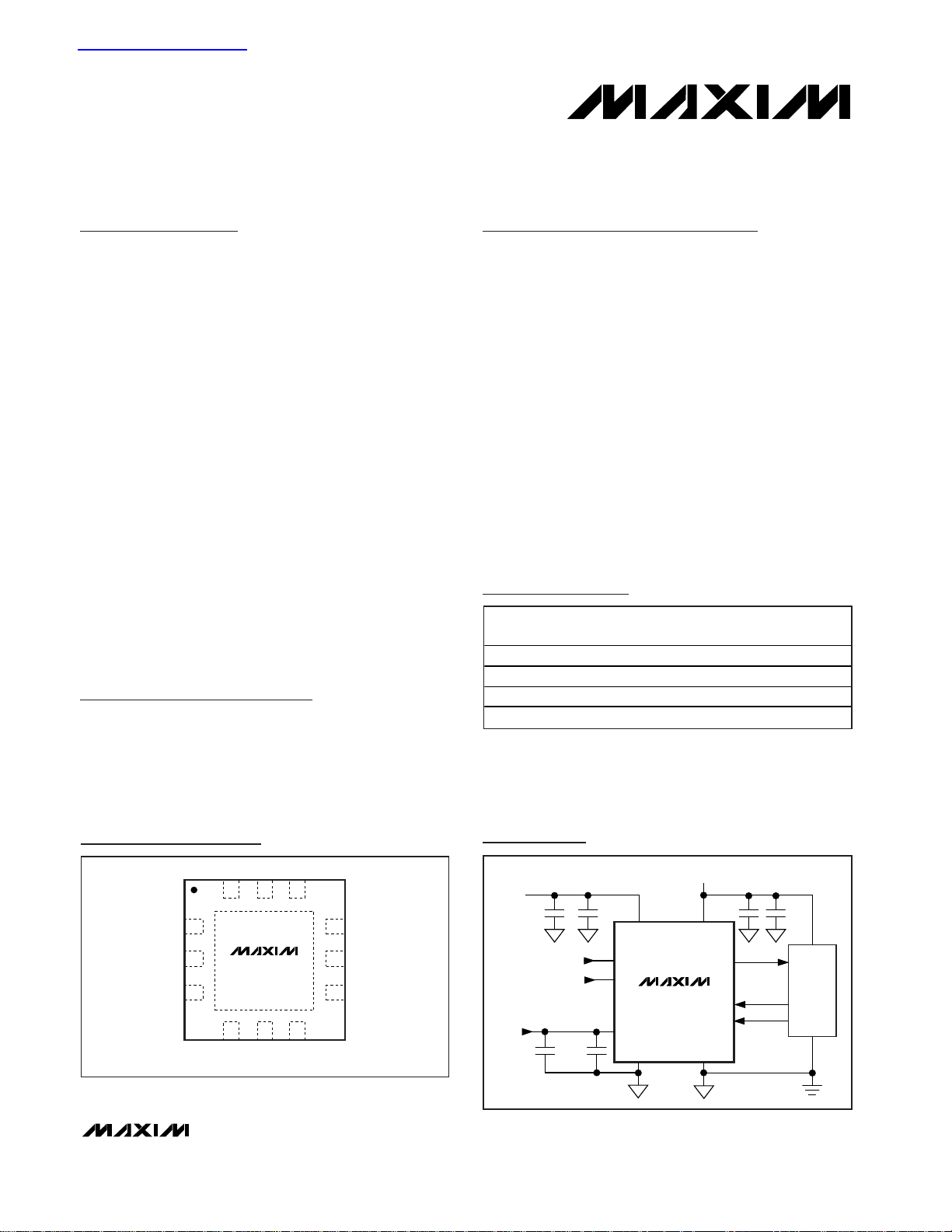
12
AIN+11N.C.10SCLK
45
N.C.6GND
1
2REF
3
9
8
7RGND
CNVST
DOUT
V
L
MAX1072
MAX1075
AIN-
V
DD
TQFN
TOP VIEW
Pin Configuration
Ordering Information
MAX1072
MAX1075
DOUT
AIN+
REF
4.7µF
10µF10µF
+4.75V TO +5.25V
0.01µF
0.01µF
0.01µF
+1.8V TO V
DD
AIN-
REF
V
DD
DIFFERENTIAL
INPUT
VOLTAGE
RGND
V
L
GND
CNVST
SCLK
µC/DSP
+
-
Typical Operating Circuit
19-3153; Rev 0; 1/04
For pricing, delivery, and ordering information, please contact Maxim/Dallas Direct! at
1-888-629-4642, or visit Maxim’s website at www.maxim-ic.com.
SPI/QSPI are trademarks of Motorola, Inc.
MICROWIRE is a trademark of National Semiconductor Corp.
查询MAX1072供应商
PART TEMP RANGE
MAX1072CTC-T 0°C to +70°C 12 TQFN-12 Unipolar
MAX1072ETC-T -40°C to +85°C 12 TQFN-12 Unipolar
MAX1075CTC-T 0°C to +70°C 12 TQFN-12 Bipolar
MAX1075ETC-T -40°C to +85°C 12 TQFN-12 Bipolar
PINPACKAGE
INPUT
MAX1072/MAX1075
1.8Msps, Single-Supply, Low-Power,
True-Differential, 10-Bit ADCs
2 _______________________________________________________________________________________
ABSOLUTE MAXIMUM RATINGS
ELECTRICAL CHARACTERISTICS
(VDD= +5V ±5%, VL= VDD, V
REF
= 4.096V, f
SCLK
= 28.8MHz, 50% duty cycle, TA= T
MIN
to T
MAX
, unless otherwise noted. Typical
values are at T
A
= +25°C.)
Stresses beyond those listed under “Absolute Maximum Ratings” may cause permanent damage to the device. These are stress ratings only, and functional
operation of the device at these or any other conditions beyond those indicated in the operational sections of the specifications is not implied. Exposure to
absolute maximum rating conditions for extended periods may affect device reliability.
VDDto GND..............................................................-0.3V to +6V
V
L
to GND ...................-0.3V to the lower of (VDD+ 0.3V) or +6V
Digital Inputs
to GND ....................-0.3V to the lower of (V
DD
+ 0.3V) or +6V
Digital Output
to GND.......................-0.3V to the lower of (V
L
+ 0.3V) or +6V
Analog Inputs and
REF to GND.............-0.3V to the lower of (V
DD
+ 0.3V) or +6V
RGND to GND .......................................................-0.3V to +0.3V
Maximum Current into Any Pin............................................50mA
Continuous Power Dissipation (T
A
= +70°C)
12-Pin TQFN (derate 16.9mW/°C above +70°C) ......1349mW
Operating Temperature Ranges
MAX107_ CTC ...................................................0°C to +70°C
MAX107_ ETC.................................................-40°C to +85°C
Junction Temperature......................................................+150°C
Storage Temperature Range .............................-60°C to +150°C
Lead Temperature (soldering, 10s) .................................+300°C
PARAMETER
CONDITIONS
UNITS
DC ACCURACY
Resolution 10 Bits
Relative Accuracy INL (Note 1)
LSB
Differential Nonlinearity DNL (Note 2)
LSB
Offset Error ±2 LSB
Offset-Error Temperature
Coefficient
±1
ppm/°C
Gain Error Offset nulled ±2 LSB
Gain Temperature Coefficient ±2
ppm/°C
DYNAMIC SPECIFICATIONS (f
IN
= 525kHz
sine wave
, VIN = V
REF
, unless otherwise noted.)
Signal-to-Noise Plus Distortion
SINAD 60 61 dB
Total Harmonic Distortion
THD -80 -74 dB
Spurious-Free Dynamic Range SFDR -80 -74 dB
Intermodulation Distortion IMD f
IN1
= 250kHz, f
IN2
= 300kHz -78 dB
Full-Power Bandwidth -3dB point, small-signal method 20
MHz
Full-Linear Bandwidth S/(N + D) Σ 56dB, single ended 2
MHz
CONVERSION RATE
Minimum Conversion Time t
CONV
(Note 3)
µs
Maximum Throughput Rate 1.8
Msps
M i ni m um Thr oug hp ut Rate ( N ote 4) 10
ksps
Track-and-Hold Acquisition Time
t
ACQ
(Note 5) 104 ns
Aperture Delay 5ns
Aperture Jitter (Note 6) 30 ps
External Clock Frequency f
SCLK
MHz
SYMBOL
MIN TYP MAX
±0.5
±0.5
0.556
28.8
MAX1072/MAX1075
1.8Msps, Single-Supply, Low-Power,
True-Differential, 10-Bit ADCs
_______________________________________________________________________________________ 3
ELECTRICAL CHARACTERISTICS (continued)
(VDD= +5V ±5%, VL= VDD, V
REF
= 4.096V, f
SCLK
= 28.8MHz, 50% duty cycle, TA= T
MIN
to T
MAX
, unless otherwise noted. Typical
values are at T
A
= +25°C.)
PARAMETER
SYMBOL
CONDITIONS
MIN
TYP
MAX
UNITS
ANALOG INPUTS (AIN+, AIN-)
AIN+ - AIN-, MAX1072 0
Differential Input Voltage Range
V
IN
AIN+ - AIN-, MAX1075
V
Absolute Input Voltage Range 0
V
DC Leakage Current ±1 µA
Input Capacitance Per input pin 20 pF
Input Current (Average)
75 µA
REFERENCE INPUT (REF)
REF Input Voltage Range V
REF
1.0
V
DD
+
V
Input Capacitance 20 pF
DC Leakage Current ±1 µA
Input Current (Average)
400 µA
DIGITAL INPUTS (SCLK, CNVST)
Input Voltage Low VIL
V
Input Voltage High VIH 0.7 x V
L
V
Input Leakage Current I
IL
µA
DIGITAL OUTPUT (DOUT)
Output Load Capacitance C
OUT
For stated timing performance 30 pF
Output Voltage Low V
OL
I
SINK
= 5mA, VL ≥ 1.8V 0.4 V
Output Voltage High V
OH
I
SOURCE
= 1mA, VL ≥ 1.8V
V
Output Leakage Current I
OL
Output high impedance
µA
POWER REQUIREMENTS
Analog Supply Voltage V
DD
V
Digital Supply Voltage V
L
1.8
V
Static, f
SCLK
= 28.8MHz
79
Static, no SCLK 4 5
Analog Supply Current,
Normal Mode
I
DD
Operational, 1.8Msps 9 11
mA
f
SCLK
= 28.8MHz 1
Analog Supply Current,
Partial Power-Down Mode
I
DD
No SCLK 1
mA
f
SCLK
= 28.8MHz 1
Analog Supply Current,
Full Power-Down Mode
I
DD
No SCLK 1
µA
Operational, full-scale input at 1.8Msps
1 2.5
Static, f
SCLK
= 28.8MHz
Partial/full power-down mode,
f
SCLK
= 28.8MHz
0.2 0.5
mA
Digital Supply Current (Note 7)
Static, no SCLK (all modes)
1
Positive-Supply Rejection PSR VDD = 5V ±5%, full-scale input
mV
Time averaged at maximum throughput rate
-V
/ 2 +V
REF
Time averaged at maximum throughput rate
V L - 0.5V
0.05 ±10
±0.2 ±10
4.75 5.25
0.4 1
0.1
±0.2 ±3.0
V
REF
REF
V
50mV
0.3 x V
V
/ 2
DD
L
DD
µA
MAX1072/MAX1075
1.8Msps, Single-Supply, Low-Power,
True-Differential, 10-Bit ADCs
4 _______________________________________________________________________________________
Note 1: Relative accuracy is the deviation of the analog value at any code from its theoretical value after the gain error and the offset
error have been nulled.
Note 2: No missing codes over temperature.
Note 3: Conversion time is defined as the number of clock cycles (16) multiplied by the clock period.
Note 4: At sample rates below 10ksps, the input full-linear bandwidth is reduced to 5kHz.
Note 5: The listed value of three SCLK cycles is given for full-speed continuous conversions. Acquisition time begins on the 14th ris-
ing edge of SCLK and terminates on the next falling edge of CNST. The IC idles in acquisition mode between conversions.
Note 6: Undersampling at the maximum signal bandwidth requires the minimum jitter spec for SINAD performance.
Note 7: Digital supply current is measured with the V
IH
level equal to VL, and the VILlevel equal to GND.
TIMING CHARACTERISTICS
(VDD= +5V ±5%, VL= VDD, V
REF
= 4.096V, f
SCLK
= 28.8MHz, 50% duty cycle, TA= T
MIN
to T
MAX
, unless otherwise noted. Typical
values are at T
A
= +25°C.)
PARAMETER
CONDITIONS
UNITS
SCLK Pulse-Width High t
CH
VL = 1.8V to V
DD
ns
SCLK Pulse-Width Low t
CL
VL = 1.8V to V
DD
ns
CL = 30pF, VL = 4.75V to V
DD
14
CL = 30pF, VL = 2.7V to V
DD
17
SCLK Rise to DOUT Transition t
DOUT
CL = 30pF, VL = 1.8V to V
DD
24
ns
DOUT Remains Valid After SCLK
VL = 1.8V to V
DD
4ns
CNVST Fall to SCLK Fall t
SETUPVL
= 1.8V to V
DD
10 ns
CNVST Pulse Width t
CSW
VL = 1.8V to V
DD
20 ns
Power-Up Time; Full Power-Down
2ms
Restart Time; Partial Power-Down
t
RCV
16
Cycles
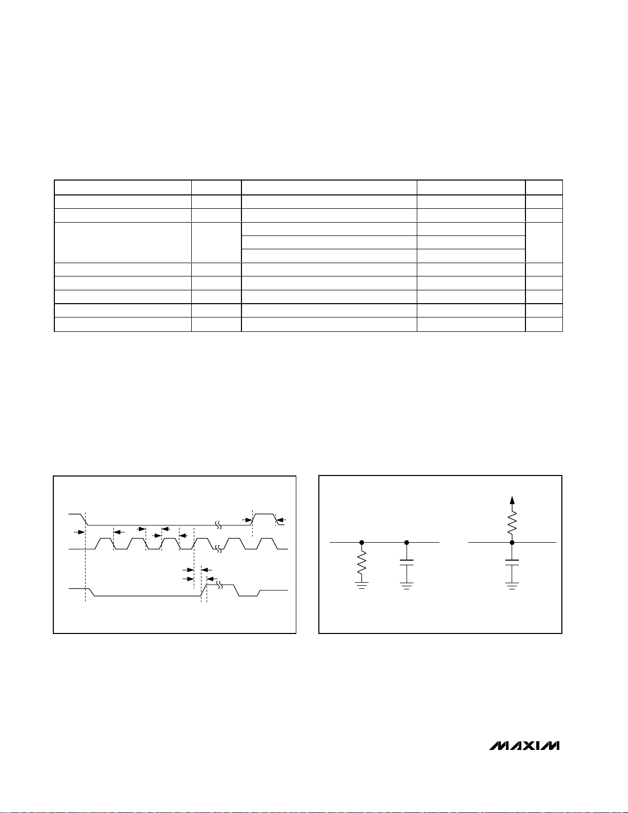
Figure 1. Detailed Serial-Interface Timing
GND
6kΩ
C
L
DOUT
DOUT
C
L
GND
V
L
a) HIGH-Z TO VOH, V
OL
TO VOH,
AND V
OH
TO HIGH-Z
b) HIGH-Z TO V
OL
, V
OH
TO VOL,
AND V
OL
TO HIGH-Z
6kΩ
Figure 2. Load Circuits for Enable/Disable Times
SYMBOL
t
DHOLD
T
PWR-UP
MIN TYP MAX
15.6
15.6
CNVST
t
SETUP
SCLK
DOUT
t
CL
t
CH
t
DHOLD
t
DOUT
t
CSW
MAX1072/MAX1075
1.8Msps, Single-Supply, Low-Power,
True-Differential, 10-Bit ADCs
_______________________________________________________________________________________ 5
Typical Operating Characteristics
(VDD= +5V, VL= VDD, V
REF
= 4.096V, f
SCLK
= 28.8MHz, TA= T
MIN
to T
MAX
, unless otherwise noted. Typical values are at TA= +25°C.)
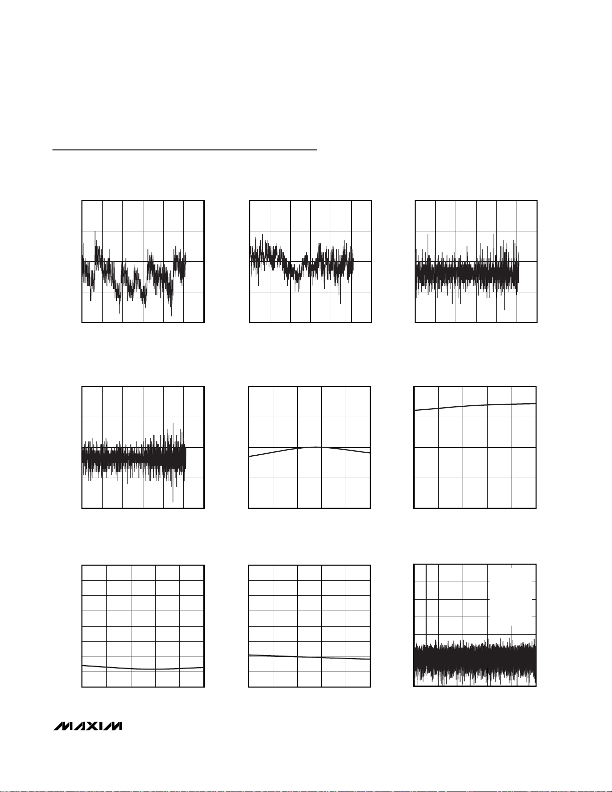
INTEGRAL NONLINEARITY
vs. DIGITAL OUTPUT CODE (MAX1072)
MAX1072/75 toc01
DIGITAL OUTPUT CODE
INL (LSB)
1000800600400200
-0.1
0
0.1
0.2
-0.2
0 1200
INTEGRAL NONLINEARITY
vs. DIGITAL OUTPUT CODE (MAX1075)
MAX1072/75 toc02
DIGITAL OUTPUT CODE
INL (LSB)
1000800600400200
-0.1
0
0.1
0.2
-0.2
0 1200
DIFFERENTIAL NONLINEARITY
vs. DIGITAL OUTPUT CODE (MAX1072)
MAX1072/75 toc03
DIGITAL OUTPUT CODE
DNL (LSB)
1000800600400200
-0.1
0
0.1
0.2
-0.2
0 1200
DIFFERENTIAL NONLINEARITY
vs. DIGITAL OUTPUT CODE (MAX1075)
MAX1072/75 toc04
DIGITAL OUTPUT CODE
DNL (LSB)
1000800600400200
-0.1
0
0.1
0.2
-0.2
0 1200
OFFSET ERROR
vs. TEMPERATURE (MAX1072)
MAX1072/75 toc05
TEMPERATURE (°C)
OFFSET ERROR (LSB)
603510-15
-0.25
0
0.25
0.50
-0.50
-40 85
OFFSET ERROR
vs. TEMPERATURE (MAX1075)
MAX1072/75 toc06
TEMPERATURE (°C)
OFFSET ERROR (LSB)
603510-15
-0.25
0
0.25
0.50
-0.50
-40 85
GAIN ERROR
vs. TEMPERATURE (MAX1072)
MAX1072/75 toc07
TEMPERATURE (°C)
GAIN ERROR (LSB)
6035-15 10
-0.75
-0.50
-0.25
0
0.25
0.50
0.75
1.00
-1.00
-40 85
GAIN ERROR
vs. TEMPERATURE (MAX1075)
MAX1072/75 toc08
TEMPERATURE (°C)
GAIN ERROR (LSB)
6035-15 10
-0.75
-0.50
-0.25
0
0.25
0.50
0.75
1.00
-1.00
-40 85
FFT PLOT (MAX1072)
MAX1072/75 toc09
ANALOG INPUT FREQUENCY (kHz)
AMPLITUDE (dB)
800600400200
-120
-100
-80
-60
-40
-20
0
-140
0 1000
f
SAMPLE
= 2Msps
f
SCLK
= 32MHz
f
IN
= 100kHz
SINAD = 61.4dB
SNR = 61.4dB
THD = -94.42dB
SFDR = 84.54dB
Typical Operating Characteristics (continued)
(VDD= +5V, VL= VDD, V
REF
= 4.096V, f
SCLK
= 28.8MHz, TA= T
MIN
to T
MAX
, unless otherwise noted. Typical values are at TA= +25°C.)
MAX1072/MAX1075
1.8Msps, Single-Supply, Low-Power,
True-Differential, 10-Bit ADCs
6 _______________________________________________________________________________________
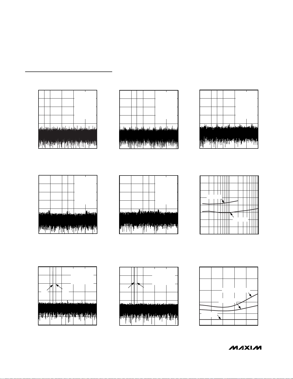
FFT PLOT (MAX1075)
MAX1072/75 toc10
ANALOG INPUT FREQUENCY (kHz)
AMPLITUDE (dB)
800600400200
-120
-100
-80
-60
-40
-20
0
-140
0 1000
f
SAMPLE
= 2Msps
f
SCLK
= 32MHz
f
IN
= 100kHz
SINAD = 61.37dB
SNR = 61.37dB
THD = -90.79dB
SFDR = 85.45dB
FFT PLOT (MAX1072)
MAX1072/75 toc11
ANALOG INPUT FREQUENCY (kHz)
AMPLITUDE (dB)
800600400200
-120
-100
-80
-60
-40
-20
0
-140
0 1000
f
SAMPLE
= 2Msps
f
SCLK
= 32MHz
f
IN
= 300kHz
SINAD = 61.43dB
SNR = 61.43dB
THD = -84.38dB
SFDR = 85.43dB
FFT PLOT (MAX1075)
MAX1072/75 toc12
ANALOG INPUT FREQUENCY (kHz)
AMPLITUDE (dB)
800600400200
-120
-100
-80
-60
-40
-20
0
-140
0 1000
f
SAMPLE
= 2Msps
f
SCLK
= 32MHz
f
IN
= 300kHz
SINAD = 61.36dB
SNR = 61.38dB
THD = -84.27dB
SFDR = 84.82dB
FFT PLOT (MAX1072)
MAX1072/75 toc13
ANALOG INPUT FREQUENCY (kHz)
AMPLITUDE (dB)
800600400200
-120
-100
-80
-60
-40
-20
0
-140
0 1000
f
SAMPLE
= 2Msps
f
SCLK
= 32MHz
f
IN
= 500kHz
SINAD = 61.27dB
SNR = 61.28dB
THD = -86.84dB
SFDR = 84.77dB
FFT PLOT (MAX1075)
MAX1072/75 toc14
ANALOG INPUT FREQUENCY (kHz)
AMPLITUDE (dB)
800600400200
-120
-100
-80
-60
-40
-20
0
-140
0 1000
f
SAMPLE
= 2Msps
f
SCLK
= 32MHz
f
IN
= 500kHz
SINAD = 61.34dB
SNR = 61.35dB
THD = -95.5dB
SFDR = 84.35dB
TOTAL HARMONIC DISTORTION
vs. SOURCE IMPEDANCE
MAX1072/75 toc15
SOURCE IMPEDANCE (Ω)
THD (dB)
100
-95
-90
-85
-80
-75
-70
-65
-60
-100
10 1000
fIN = 100kHz
fIN = 500kHz
TWO-TONE IMD PLOT (MAX1072)
MAX1072/75 toc16
ANALOG INPUT FREQUENCY (kHz)
AMPLITUDE (dB)
800600400200
-120
-100
-80
-60
-40
-20
0
-140
0 1000
f
SCLK
= 32MHz
f
IN1
= 250.039kHz
f
IN2
= 300.059kHz
IMD = -81.9dB
f
IN1
f
IN2
TWO-TONE IMD PLOT (MAX1075)
MAX1072/75 toc17
ANALOG INPUT FREQUENCY (kHz)
AMPLITUDE (dB)
800600400200
-120
-100
-80
-60
-40
-20
0
-140
0 1000
f
SCLK
= 32MHz
f
IN1
= 250.039kHz
f
IN2
= 300.059kHz
IMD = -82.1dB
f
IN1
f
IN2
VDD/VL FULL POWER-DOWN
SUPPLY CURRENT vs. TEMPERATURE
MAX1072/75 toc18
TEMPERATURE (°C)
V
DD
/V
L
SUPPLY CURRENT (µA)
603510-15
0.2
0.4
0.6
0.8
1.0
0
-40 85
VDD, f
SCLK
= 28.8MHz
VDD, f
SCLK
= 0
VL, f
SCLK
= 0

MAX1072/MAX1075
1.8Msps, Single-Supply, Low-Power,
True-Differential, 10-Bit ADCs
_______________________________________________________________________________________ 7
Typical Operating Characteristics (continued)
(VDD= +5V, VL= VDD, V
REF
= 4.096V, f
SCLK
= 28.8MHz, TA= T
MIN
to T
MAX
, unless otherwise noted. Typical values are at TA= +25°C.)
VL PARTIAL/FULL POWER-DOWN
SUPPLY CURRENT vs. TEMPERATURE
MAX1072/75 toc19
TEMPERATURE (°C)
V
L
SUPPLY CURRENT (µA)
603510-15
50
100
150
200
0
-40 85
VL = 3V
f
SCLK
= 28.8MHz
VL = 5V
f
SCLK
= 28.8MHz
VDD SUPPLY CURRENT
vs. TEMPERATURE
MAX1072/75 toc20
TEMPERATURE (°C)
V
DD
SUPPLY CURRENT (mA)
603510-15
3
6
9
12
0
-40 85
CONVERTING
f
SCLK
= 28.8MHz
PARTIAL POWER-DOWN
f
SCLK
= 28.8MHz
VDD SUPPLY CURRENT
vs. CONVERSION RATE
MAX072/75 toc21
f
SAMPLE
(kHz)
V
DD
SUPPLY CURRENT (mA)
15001000500
3
6
9
12
0
0 2000
VL SUPPLY CURRENT
vs. TEMPERATURE
MAX1072/75 toc22
TEMPERATURE (°C)
V
L
SUPPLY CURRENT (mA)
603510-15
0.2
0.4
0.6
0.8
1.0
0
-40 85
CONVERTING
f
SCLK
= 28.8MHz
FULL/PARTIAL
POWER-DOWN
f
SCLK
= 28.8MHz
VL SUPPLY CURRENT
vs. CONVERSION RATE
MAX1072/75 toc23
f
SAMPLE
(kHz)
V
L
SUPPLY CURRENT (mA)
15001000500
0.3
0.5
0.8
1.0
0
0 2000
VL = 5V
VL = 3V
VL = 1.8V

MAX1072/MAX1075
1.8Msps, Single-Supply, Low-Power,
True-Differential, 10-Bit ADCs
8 _______________________________________________________________________________________
Pin Description
PIN NAME FUNCTION
1 AIN- Negative Analog Input
2 REF
External Reference Voltage Input. V
REF
sets the analog input range. Bypass REF with a 0.01µF
capacitor and a 4.7µF capacitor to RGND.
3 RGND Reference Ground. Connect RGND to GND.
4V
DD
Positive Analog Supply Voltage (+4.75V to +5.25V). Bypass VDD with a 0.01µF capacitor and a 10µF
capacitor to GND.
5, 11 N.C. No Connection
6 GND Ground. GND is internally connected to EP.
7V
L
Positive Logic Supply Voltage (1.8V to VDD). Bypass VL with a 0.01µF capacitor and a 10µF capacitor
to GND.
8 DOUT Serial Data Output. Data is clocked out on the rising edge of SCLK.
9 CNVST
Convert Start. Forcing CNVST high prepares the part for a conversion. Conversion begins on the
falling edge of CNVST. The sampling instant is defined by the falling edge of CNVST.
10 SCLK Serial Clock Input. Clocks data out of the serial interface. SCLK also sets the conversion speed.
12 AIN+ Positive Analog Input
— EP Exposed Paddle. EP is internally connected to GND.
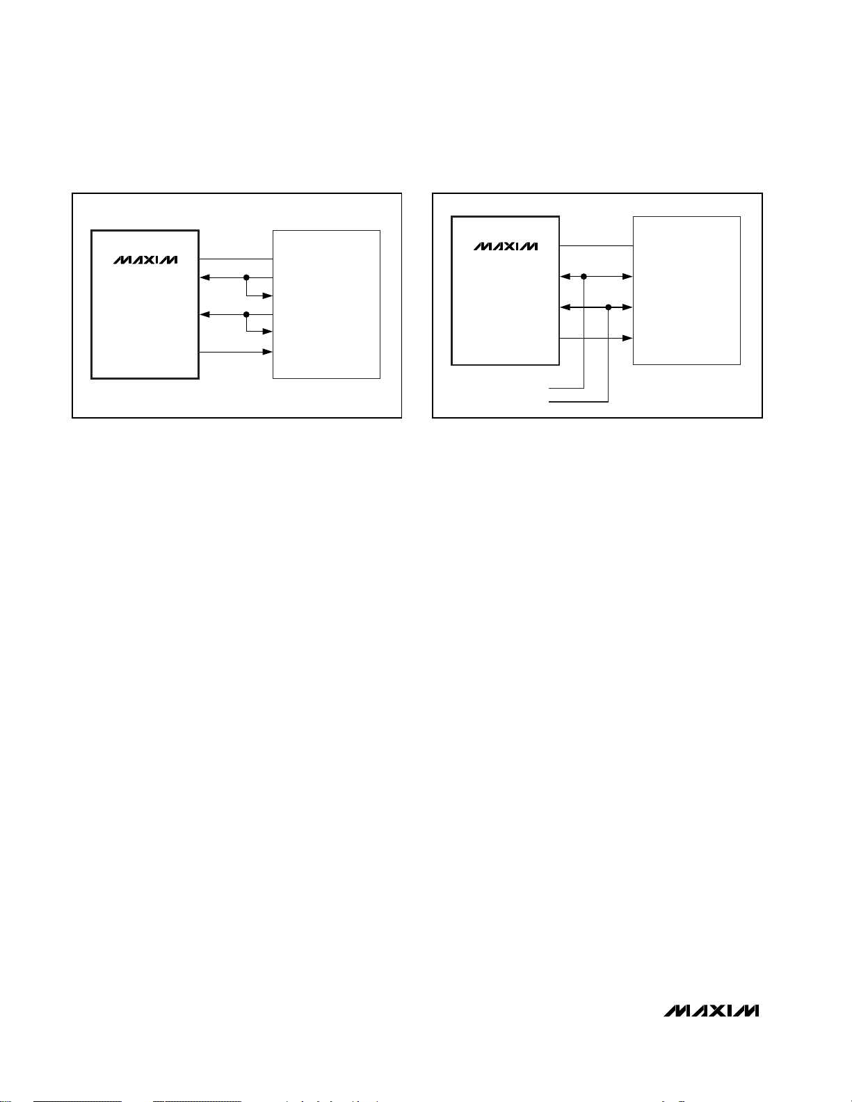
Detailed Description
The MAX1072/MAX1075 use an input T/H and successive-approximation register (SAR) circuitry to convert
an analog input signal to a digital 10-bit output. The
serial interface requires only three digital lines (SCLK,
CNVST, and DOUT) and provides easy interfacing to
microprocessors (µPs) and DSPs. Figure 3 shows the
simplified internal structure for the MAX1072/MAX1075.
True-Differential Analog Input T/H
The equivalent circuit of Figure 4 shows the input architecture of the MAX1072/MAX1075, which is composed of
a T/H, a comparator, and a switched-capacitor digital-toanalog converter (DAC). The T/H enters its tracking mode
on the 14th SCLK rising edge of the previous conversion.
Upon power-up, the T/H enters its tracking mode immediately. The positive input capacitor is connected to AIN+.
The negative input capacitor is connected to AIN-. The
T/H enters its hold mode on the falling edge of CNVST
and the difference between the sampled positive and
negative input voltages is converted. The time required
for the T/H to acquire an input signal is determined by
how quickly its input capacitance is charged. If the input
signal’s source impedance is high, the acquisition time
lengthens. The acquisition time, t
ACQ
, is the minimum
time needed for the signal to be acquired. It is calculated
by the following equation:
t
ACQ
≥ 8 × (RS + RIN) × 16pF
where RIN= 200Ω, and RS is the source impedance of
the input signal.
Note: t
ACQ
is never less than 104ns and any source
impedance below 12Ω does not significantly affect the
ADC’s AC performance.
Input Bandwidth
The ADC’s input-tracking circuitry has a 20MHz smallsignal bandwidth, making it is possible to digitize highspeed transient events and measure periodic signals
with bandwidths exceeding the ADC’s sampling rate by
using undersampling techniques. To avoid high-frequency signals being aliased into the frequency band
of interest, anti-alias filtering is recommended.
Analog Input Protection
Internal protection diodes that clamp the analog input
to VDDand GND allow the analog input pins to swing
from GND - 0.3V to VDD+ 0.3V without damage. Both
inputs must not exceed VDDor be lower than GND for
accurate conversions.

MAX1072/MAX1075
1.8Msps, Single-Supply, Low-Power,
True-Differential, 10-Bit ADCs
_______________________________________________________________________________________ 9
Serial Interface
Initialization After Power-Up
and Starting a Conversion
Upon initial power-up, the MAX1072/MAX1075 require a
complete conversion cycle to initialize the internal calibration. Following this initial conversion, the part is ready
for normal operation. This initialization is only required
after a hardware power-up sequence and is not required
after exiting partial or full power-down mode.
To start a conversion, pull CNVST low. At CNVST’s
falling edge, the T/H enters its hold mode and a conversion is initiated. SCLK runs the conversion and the
data can then be shifted out serially on DOUT.
Timing and Control
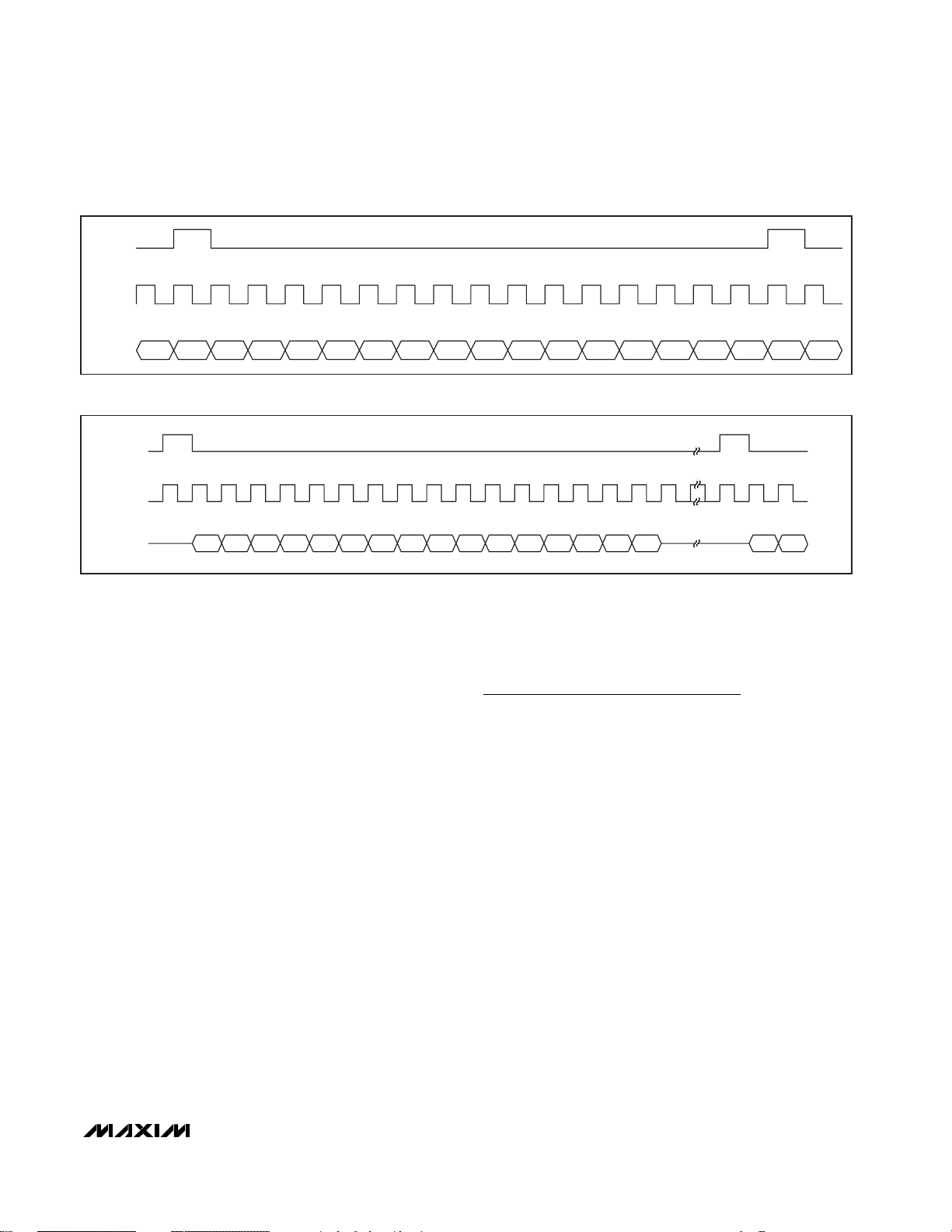
Conversion-start and data-read operations are controlled by the CNVST and SCLK digital inputs. Figures
1 and 5 show timing diagrams, which outline the serialinterface operation.
A CNVST falling edge initiates a conversion sequence;
the T/H stage holds the input voltage, the ADC begins
to convert, and DOUT changes from high impedance
to logic low. SCLK is used to drive the conversion
process, and it shifts data out as each bit of the conversion is determined.
SCLK begins shifting out the data after the 4th rising
edge of SCLK. DOUT transitions t
DOUT
after each
SCLK’s rising edge and remains valid 4ns (t
DHOLD
)
after the next rising edge. The 4th rising clock edge
produces the MSB of the conversion at DOUT, and the
MSB remains valid 4ns after the 5th rising edge. Since
there are 10 data bits, 2 sub-bits (S1 and S0), and 3
leading zeros, at least 16 rising clock edges are needed to shift out these bits. For continuous operation, pull
CNVST high between the 14th and the 16th SCLK rising edges. If CNVST stays low after the falling edge of
the 16th SCLK cycle, the DOUT line goes to a highimpedance state on either CNVST’s rising edge or the
next SCLK’s rising edge.
Partial Power-Down and
Full Power-Down Modes
Power consumption can be reduced significantly by
placing the MAX1072/MAX1075 in either partial powerdown mode or full power-down mode. Partial powerdown mode is ideal for infrequent data sampling and
fast wake-up time applications. Pull CNVST high after
the 3rd SCLK rising edge and before the 14th SCLK
rising edge to enter and stay in partial power-down
mode (see Figure 6). This reduces the supply current
to 1mA. Drive CNVST low and allow at least 14 SCLK
cycles to elapse before driving CNVST high to exit partial power-down mode.
Full power-down mode is ideal for infrequent data sampling and very low supply current applications. The
MAX1072/MAX1075 have to be in partial power-down
mode in order to enter full power-down mode. Perform the
SCLK/CNVST sequence described above to enter partial
RGND
AIN +
GND
DOUT
SCLK
CNVST
CONTROL
LOGIC AND
TIMING
AIN -
V
L
V
DD
REF
10-BIT
SAR
ADC
MAX1072
MAX1075
T/H
OUTPUT
BUFFER
Figure 3. Functional Diagram
C
IN+
R
IN+
R
IN-
C
IN-
V
AZ
AIN+
AIN-
CONTROL
LOGIC
CAPACITIVE
DAC
COMP
C
IN+
R
IN+
R
IN-
C
IN-
V
AZ
AIN+
AIN-
CONTROL
LOGIC
CAPACITIVE
DAC
COMP
ACQUISITION MODE
HOLD/CONVERSION MODE
Figure 4. Equivalent Input Circuit

MAX1072/MAX1075
power-down mode. Then repeat the same sequence to
enter full power-down mode (see Figure 7). Drive CNVST
low, and allow at least 14 SCLK cycles to elapse before
driving CNVST high to exit full power-down mode. In partial/full power-down mode, maintain a logic low or a logic
high on SCLK to minimize power consumption.
Transfer Function
Figure 8 shows the unipolar transfer function for the
MAX1072. Figure 9 shows the bipolar transfer function for
the MAX1075. The MAX1072 output is straight binary,
while the MAX1075 output is two’s complement.
1.8Msps, Single-Supply, Low-Power,
True-Differential, 10-Bit ADCs
10 ______________________________________________________________________________________
DOUT
MODE
SCLK
CNVST
DOUT GOES HIGH IMPEDANCE ONCE CNVST GOES HIGH
CNVST MUST GO HIGH AFTER THE 3RD BUT BEFORE THE 14TH SCLK RISING EDGE
ONE 8-BIT TRANSFER
1ST SCLK RISING EDGE
PPD
0 0 0 D9D8D7D6D5
NORMAL
Figure 6. SPI Interface—Partial Power-Down Mode
Figure 5. Interface-Timing Sequence
Figure 7. SPI Interface—Full Power-Down Mode
t
ACQUIRE
CONTINUOUS-CONVERSION
SELECTION WINDOW
CNVST
t
SETUP
DOUT
SCLK
41412 83 16
HIGH IMPEDANCE
S1D2D4 D3D7 D6 D5D9 D8
POWER-MODE SELECTION WINDOW
S0D0D1
CNVST
SCLK
DOUT
(MODE)
FIRST 8-BIT TRANSFER
1ST SCLK RISING EDGE 1ST SCLK RISING EDGE
0 0 0 D9D8 D7D6D5
EXECUTE PARTIAL POWER-DOWN TWICE
SECOND 8-BIT TRANSFER
DOUT ENTERS TRI-STATE ONCE CNVST GOES HIGH
000000
0
0
FPDRECOVERYPPDNORMAL

Applications Information
External Reference
An external reference is required for the MAX1072/
MAX1075. Use a 4.7µF and 0.01µF bypass capacitor on
the REF pin for best performance. The reference input
structure allows a voltage range of +1V to VDD.
How to Start a Conversion
An analog-to-digital conversion is initiated by CNVST,
clocked by SCLK, and the resulting data is clocked out
on DOUT by SCLK. With SCLK idling high or low, a
falling edge on CNVST begins a conversion. This causes
the analog input stage to transition from track to hold
mode, and DOUT to transition from high impedance to
being actively driven low. A total of 16 SCLK cycles are
required to complete a normal conversion. If CNVST is
low during the 16th falling SCLK edge, DOUT returns to
high impedance on the next rising edge of CNVST or
SCLK, enabling the serial interface to be shared by multiple devices. If CNVST returns high after the 14th, but
before the 16th SCLK rising edge, DOUT remains active
so continuous conversions can be sustained. The highest throughput is achieved when performing continuous
conversions. Figure 10 illustrates a conversion using a
typical serial interface.
Connection to
Standard Interfaces
The MAX1072/MAX1075 serial interface is fully compatible with SPI/QSPI and MICROWIRE (see Figure 11). If a
serial interface is available, set the CPU’s serial interface
in master mode so the CPU generates the serial clock.
Choose a clock frequency up to 28.8MHz.
SPI and MICROWIRE
When using SPI or MICROWIRE, the MAX1072/MAX1075
are compatible with all four modes programmed with the
CPHA and CPOL bits in the SPI or MICROWIRE control
register. Conversion begins with a CNVST falling edge.
DOUT goes low, indicating a conversion is in progress.
Two consecutive 1-byte reads are required to get the full
10 bits from the ADC. DOUT transitions on SCLK rising
edges. DOUT is guaranteed to be valid t
DOUT
later and
remains valid until t
DHOLD
after the following SCLK rising
edge. When using CPOL = 0 and CPHA = 0 or CPOL = 1
and CPHA = 1, the data is clocked into the µP on the
following rising edge. When using CPOL = 0 and CPHA
= 1 or CPOL = 1 and CPHA = 0, the data is clocked
into the µP on the next falling edge. See Figure 11 for
connections and Figures 12 and 13 for timing. See the
Timing Characteristics section to determine the best
mode to use.
MAX1072/MAX1075
1.8Msps, Single-Supply, Low-Power,
True-Differential, 10-Bit ADCs
______________________________________________________________________________________ 11
OUTPUT CODE
FULL-SCALE
TRANSITION
111...111
12 3
0
FS
FS - 3/2 LSB
FS = V
REF
DIFFERENTIAL INPUT
VOLTAGE (LSB)
1 LSB =
V
REF
1024
111...110
111...101
000...011
000...010
000...001
000...000
ZS = 0
Figure 8. Unipolar Transfer Function (MAX1072 Only)
OUTPUT CODE
FULL-SCALE
TRANSITION
FS0FS
FS - 3/2 LSB
DIFFERENTIAL INPUT
VOLTAGE (LSB)
011...111
011...110
000...010
000...001
000...000
111...111
111...110
111...101
100...001
100...000
1 LSB =
V
REF
1024
FS =
V
REF
2
- FS =
-V
REF
2
ZS = 0
Figure 9. Bipolar Transfer Function (MAX1075 Only)

MAX1072/MAX1075
1.8Msps, Single-Supply, Low-Power,
True-Differential, 10-Bit ADCs
12 ______________________________________________________________________________________
0 0 0 D9D8D7D6D5D4D3D2D1D0S1S0 0
DOUT
SCLK
CNVST
0
1
1
1614
Figure 10. Continuous Conversion with Burst/Continuous Clock
Figure 11. Common Serial-Interface Connections to the MAX1072/MAX1075
MAX1072
MAX1075
+3V TO +5V
CNVST
SCLK
DOUT
I/O
SCK
MISO
SS
A) SPI
MAX1072
MAX1075
+3V TO +5V
CNVST
SCLK
DOUT
CS
SCK
MISO
SS
B) QSPI
MAX1072
MAX1075
CNVST
SCLK
DOUT
I/O
SK
SI
C) MICROWIRE

MAX1072/MAX1075
1.8Msps, Single-Supply, Low-Power,
True-Differential, 10-Bit ADCs
______________________________________________________________________________________ 13
QSPI
Unlike SPI, which requires two 1-byte reads to acquire
the 10 bits of data from the ADC, QSPI allows the minimum number of clock cycles necessary to clock in the
data. The MAX1072/MAX1075 require 16 clock cycles
from the µP to clock out the 10 bits of data. Figure 14
shows a transfer using CPOL = 1 and CPHA = 1. The
conversion result contains three zeros, followed by the
10 data bits, 2 sub-bits, and a trailing zero with the data
in MSB-first format.
DSP Interface to the TMS320C54_
The MAX1072/MAX1075 can be directly connected
to the TMS320C54_ family of DSPs from Texas
Instruments, Inc. Set the DSP to generate its own
clocks or use external clock signals. Use either the
standard or buffered serial port. Figure 15 shows the
simplest interface between the MAX1072/MAX1075 and
the TMS320C54_, where the transmit serial clock
(CLKX) drives the receive serial clock (CLKR) and
SCLK, and the transmit frame sync (FSX) drives the
receive frame sync (FSR) and CNVST.
SCLK
DOUT
916
8
1
D0
D9
D8
D6
D5
D4
D3
D2
D1
D7
HIGH-Z
HIGH-Z
CNVST
S1
S0
Figure 13. SPI/MICROWIRE Serial-Interface Timing—Continuous Conversion (CPOL = CPHA = 0), (CPOL = CPHA = 1)
0 0 0 D9D8D7D6D5D4D3D2D1D0S1S0 0
DOUT
SCLK
CNVST
0
1
1
14
16
Figure 12. SPI/MICROWIRE Serial-Interface Timing—Single Conversion (CPOL = CPHA = 0), (CPOL = CPHA = 1)
Figure 14. QSPI Serial-Interface Timing—Single Conversion (CPOL = 1, CPHA = 1)
SCLK
DOUT
CNVST
16
S0
S1
D9
D8
D4D5D6 D3 D2 D1 D0
HIGH-Z
D7
HIGH-Z
2
For continuous conversion, set the serial port to transmit a clock, and pulse the frame sync signal for a clock
period before data transmission. The serial-port configuration (SPC) register should be set up with internal
frame sync (TXM = 1), CLKX driven by an on-chip clock
source (MCM = 1), burst mode (FSM = 1), and 16-bit
word length (FO = 0).
This setup allows continuous conversions provided that
the data transmit register (DXR) and the data-receive
register (DRR) are serviced before the next conversion.
Alternatively, autobuffering can be enabled when using
the buffered serial port to execute conversions and
read the data without CPU intervention. Connect the V
L
pin to the TMS320C54_ supply voltage when the
MAX1072/MAX1075 are operating with an analog supply voltage higher than the DSP supply voltage. The
word length can be set to 8 bits with FO = 1 to implement the power-down modes. The CNVST pin must idle
high to remain in either power-down state.
Another method of connecting the MAX1072/MAX1075
to the TMS320C54_ is to generate the clock signals
external to either device. This connection is shown in
Figure 16 where serial clock (CLOCK) drives the CLKR
and SCLK and the convert signal (CONVERT) drives
the FSR and CNVST.
The serial port must be set up to accept an external
receive-clock and external receive-frame sync.
The SPC register should be written as follows:
TXM = 0, external frame sync
MCM = 0, CLKX is taken from the CLKX pin
FSM = 1, burst mode
FO = 0, data transmitted/received as 16-bit words
This setup allows continuous conversion, provided that
the DRR is serviced before the next conversion.
Alternatively, autobuffering can be enabled when using
the buffered serial port to read the data without CPU
intervention. Connect the VL pin to the TMS320C54_
supply voltage when the MAX1072/MAX1075 are operating with an analog supply voltage higher than the
DSP supply voltage.
The MAX1072/MAX1075 can also be connected to the
TMS320C54_ by using the data transmit (DX) pin to
drive CNVST and the CLKX generated internally to
drive SCLK. A pullup resistor is required on the CNVST
signal to keep it high when DX goes high impedance
and 0001hex should be written to the DXR continuously
for continuous conversions. The power-down modes
may be entered by writing 00FFhex to the DXR (see
Figures 17 and 18).
DSP Interface to the ADSP21_ _ _
The MAX1072/MAX1075 can be directly connected to
the ADSP21_ _ _ family of DSPs from Analog Devices,
Inc. Figure 19 shows the direct connection of the
MAX1072/MAX1075 to the ADSP21_ _ _. There are two
modes of operation that can be programmed to interface
with the MAX1072/MAX1075. For continuous conversions, idle CNVST low and pulse it high for one clock
cycle during the LSB of the previous transmitted word.
The ADSP21_ _ _ STCTL and SRCTL registers should be
configured for early framing (LAFR = 0) and for an
active-high frame (LTFS = 0, LRFS = 0) signal. In this
mode, the data-independent frame-sync bit (DITFS = 1)
can be selected to eliminate the need for writing to the
transmit-data register more than once. For single conversions, idle CNVST high and pulse it low for the entire
conversion. The ADSP21_ _ _ STCTL and SRCTL regis-
MAX1072/MAX1075
1.8Msps, Single-Supply, Low-Power,
True-Differential, 10-Bit ADCs
14 ______________________________________________________________________________________
Figure 15. Interfacing to the TMS320C54_ Internal Clocks
Figure 16. Interfacing to the TMS320C54_ External Clocks
MAX1072
MAX1075
TMS320C54_
V
L
SCLK
CNVST
DOUT
DV
DD
CLKR
FSR
CLKX
FSX
DR
V
L DV
MAX1072
MAX1075
SCLK
DD
TMS320C54_
CLKR
CNVST
DOUT DR
CLOCK
CONVERT
FSR
MAX1072/MAX1075
1.8Msps, Single-Supply, Low-Power,
True-Differential, 10-Bit ADCs
______________________________________________________________________________________ 15
ters should be configured for late framing (LAFR = 1)
and for an active-low frame (LTFS = 1, LRFS = 1) signal.
This is also the best way to enter the power-down modes
by setting the word length to 8 bits (SLEN = 1001).
Connect the VL pin to the ADSP21_ _ _ supply voltage
when the MAX1072/MAX1075 are operating with a supply voltage higher than the DSP supply voltage (see
Figures 17 and 18).
Layout, Grounding, and Bypassing
For best performance, use PC boards. Wire-wrap
boards are not recommended. Board layout should
ensure that digital and analog signal lines are separated from each other. Do not run analog and digital
(especially clock) lines parallel to one another, or digital
lines underneath the ADC package.
Figure 20 shows the recommended system ground
connections. Establish a single-point analog ground
(star ground point) at GND, separate from the logic
ground. Connect all other analog grounds and DGND
to this star ground point for further noise reduction. The
ground return to the power supply for this ground
should be low impedance and as short as possible for
noise-free operation.
High-frequency noise in the V
DD
power supply can
affect the ADC’s high-speed comparator. Bypass this
supply to the single-point analog ground with 0.01µF
and 10µF bypass capacitors. Minimize capacitor lead
lengths for best supply-noise rejection.
Definitions
Integral Nonlinearity
Integral nonlinearity (INL) is the deviation of the values on
an actual transfer function from a straight line. This
straight line can be either a best-straight-line fit or a line
drawn between the end points of the transfer function,
once offset and gain errors have been nullified. The static
linearity parameters for the MAX1072/MAX1075 are measured using the end-points method.
Differential Nonlinearity
Differential nonlinearity (DNL) is the difference between
an actual step width and the ideal value of 1 LSB. A DNL
error specification of 1 LSB or less guarantees no missing
codes and a monotonic transfer function.
Aperture Jitter
Aperture jitter (tAJ) is the sample-to-sample variation in
the time between the samples.
Aperture Delay
Aperture delay (tAD) is the time defined between the
falling edge of CNVST and the instant when an actual
sample is taken.
0 0 0 D9D8D7D6D5D4D3D2D1D0S1S0 0
DOUT
SCLK
CNVST
00S0
1 1
Figure 17. DSP Interface—Continuous Conversion
000D9D8D7D6D5D4D3D2D1D0S1S00
DOUT
SCLK
CNVST
0 0
1
1
Figure 18. DSP Interface—Single-Conversion, Continuous/Burst Clock

MAX1072/MAX1075
Signal-to-Noise Ratio
For a waveform perfectly reconstructed from digital samples, signal-to-noise ratio (SNR) is the ratio of full-scale
analog input (RMS value) to the RMS quantization error
(residual error). The theoretical minimum analog-to-digital
noise is caused by quantization error, and results directly
from the ADC’s resolution (N bits):
SNR = (6.02 x N + 1.76)dB
In reality, there are other noise sources besides quantization noise, including thermal noise, reference noise, clock
jitter, etc. Therefore, SNR is computed by taking the ratio
of the RMS signal to the RMS noise, which includes all
spectral components minus the fundamental, the first five
harmonics, and the DC offset.
Signal-to-Noise Plus Distortion
Signal-to-noise plus distortion (SINAD) is the ratio of the
fundamental input frequency’s RMS amplitude to the
RMS equivalent of all other ADC output signals:
SINAD(dB) = 20 x log (Signal
RMS
/ Noise
RMS
)
Effective Number of Bits
Effective number of bits (ENOB) indicates the global
accuracy of an ADC at a specific input frequency and
sampling rate. An ideal ADC’s error consists of quantization noise only. With an input range equal to the full-scale
range of the ADC, calculate the ENOB as follows:
Total Harmonic Distortion
Total harmonic distortion (THD) is the ratio of the RMS
sum of the first five harmonics of the input signal to the
fundamental itself. This is expressed as:
where V
1
is the fundamental amplitude, and V2through
V5are the amplitudes of the 2nd- through 5th-order
harmonics.
Spurious-Free Dynamic Range
Spurious-free dynamic range (SFDR) is the ratio of the
RMS amplitude of the fundamental (maximum signal
component) to the RMS value of the next largest distortion component.
Full-Power Bandwidth
Full-power bandwidth is the frequency at which the input
signal amplitude attenuates by 3dB for a full-scale input.
THD x
VVVV
V
log=
+++
20
2232425
2
1
ENOB
SINAD
( .)
.
=
− 176
602
1.8Msps, Single-Supply, Low-Power,
True-Differential, 10-Bit ADCs
16 ______________________________________________________________________________________
MAX1072
MAX1075
ADSP21_ _ _
V
L
SCLK
CNVST
DOUT
VDDINT
RCLK
RFS
TCLK
TFS
DR
Figure 19. Interfacing to the ADSP21_ _ _
10µF
0.1µF
10µF
0.1µF
V
DD
GND V
L
SUPPLIES
DGND V
L
DIGITAL
CIRCUITRY
V
DD
GND RGND
V
L
MAX1072
MAX1075
Figure 20. Power-Supply Grounding Condition

Full-Linear Bandwidth
Full-linear bandwidth is the frequency at which the signal to noise plus distortion (SINAD) is equal to 56dB.
Intermodulation Distortion
Any device with nonlinearities creates distortion products when two sine waves at two different frequencies
(f1 and f2) are input into the device. Intermodulation
distortion (IMD) is the total power of the IM2 to IM5
intermodulation products to the Nyquist frequency relative to the total input power of the two input tones, f1
and f2. The individual input tone levels are at -7dBFS.
The intermodulation products are as follows:
• 2nd-order intermodulation products (IM2): f1+ f2,
f2- f
1
• 3rd-order intermodulation products (IM3): 2f1- f2,
2f2- f1, 2f1+ f2, 2f2+ f
1
• 4th-order intermodulation products (IM4): 3f1- f2,
3f2- f1, 3f1+ f2, 3f2+ f
1
• 5th-order intermodulation products (IM5): 3f1- 2f2,
3f2- 2f1, 3f1+ 2f2, 3f2+ 2f
1
MAX1072/MAX1075
1.8Msps, Single-Supply, Low-Power,
True-Differential, 10-Bit ADCs
______________________________________________________________________________________ 17
Chip Information
TRANSISTOR COUNT: 13,016
PROCESS: BiCMOS

MAX1072/MAX1075
1.8Msps, Single-Supply, Low-Power,
True-Differential, 10-Bit ADCs
Maxim cannot assume responsibility for use of any circuitry other than circuitry entirely embodied in a Maxim product. No circuit patent licenses are
implied. Maxim reserves the right to change the circuitry and specifications without notice at any time.
18 ____________________Maxim Integrated Products, 120 San Gabriel Drive, Sunnyvale, CA 94086 408-737-7600
© 2004 Maxim Integrated Products Printed USA is a registered trademark of Maxim Integrated Products.
Package Information
(The package drawing(s) in this data sheet may not reflect the most current specifications. For the latest package outline information
go to www.maxim-ic.com/packages
.)
24L QFN THIN.EPS
PACKAGE OUTLINE
12,16,20,24L QFN THIN, 4x4x0.8 mm
21-0139
PACKAGE OUTLINE
12,16,20,24L QFN THIN, 4x4x0.8 mm
21-0139
1
B
2
2
B
2
 Loading...