

Page 1
MAX1069
58.6ksps, 14-Bit, 2-Wire Serial ADC
in a 14-Pin TSSOP
________________________________________________________________ Maxim Integrated Products 1
19-2652; Rev 0; 10/02
For pricing, delivery, and ordering information, please contact Maxim/Dallas Direct! at
1-888-629-4642, or visit Maxim’s website at www.maxim-ic.com.
General Description
The MAX1069 is a low-power, 14-bit successiveapproximation analog-to-digital converter (ADC). The
device features automatic power-down, an on-chip
4MHz clock, a +4.096V internal reference, and an
I2C™-compatible 2-wire serial interface capable of both
fast and high-speed modes.
The MAX1069 operates from a single supply and consumes 5mW at the maximum conversion rate of
58.6ksps. AutoShutdown™ powers down the device
between conversions, reducing supply current to less
than 50µA at a 1ksps throughput rate. The option of a
separate digital supply voltage allows direct interfacing
with +2.7V to +5.5V digital logic.
The MAX1069 performs a unipolar conversion on its
single analog input using its internal 4MHz clock. The
full-scale analog input range is determined by the internal reference or by an externally applied reference voltage ranging from 1V to AV
DD
.
The four address select inputs (ADD0–ADD3) allow up
to sixteen MAX1069 devices on the same bus.
The MAX1069 is packaged in a 14-pin TSSOP and
offers both commercial and extended temperature
ranges. Refer to the MAX1169 for a 16-bit device in a
pin-compatible package.
Applications
Hand-Held Portable Applications
Medical Instruments
Battery-Powered Test Equipment
Solar-Powered Remote Systems
Receive Signal Strength Indicators
System Supervision
Features
♦ High-Speed I2C-Compatible Serial Interface
400kHz Fast Mode
1.7MHz High-Speed Mode
♦ +4.75V to +5.25V Single Supply
♦ +2.7V to +5.5V Adjustable Logic Level
♦ Internal +4.096V Reference
♦ External Reference: 1V to AV
DD
♦ Internal 4MHz Conversion Clock
♦ 58.6ksps Sampling Rate
♦ AutoShutdown Between Conversions
♦ Low Power
5.0mW at 58.6ksps
4.2mW at 50ksps
2.0mW at 10ksps
0.23mW at 1ksps
3µW in Shutdown
♦ Small 14-Pin TSSOP Package
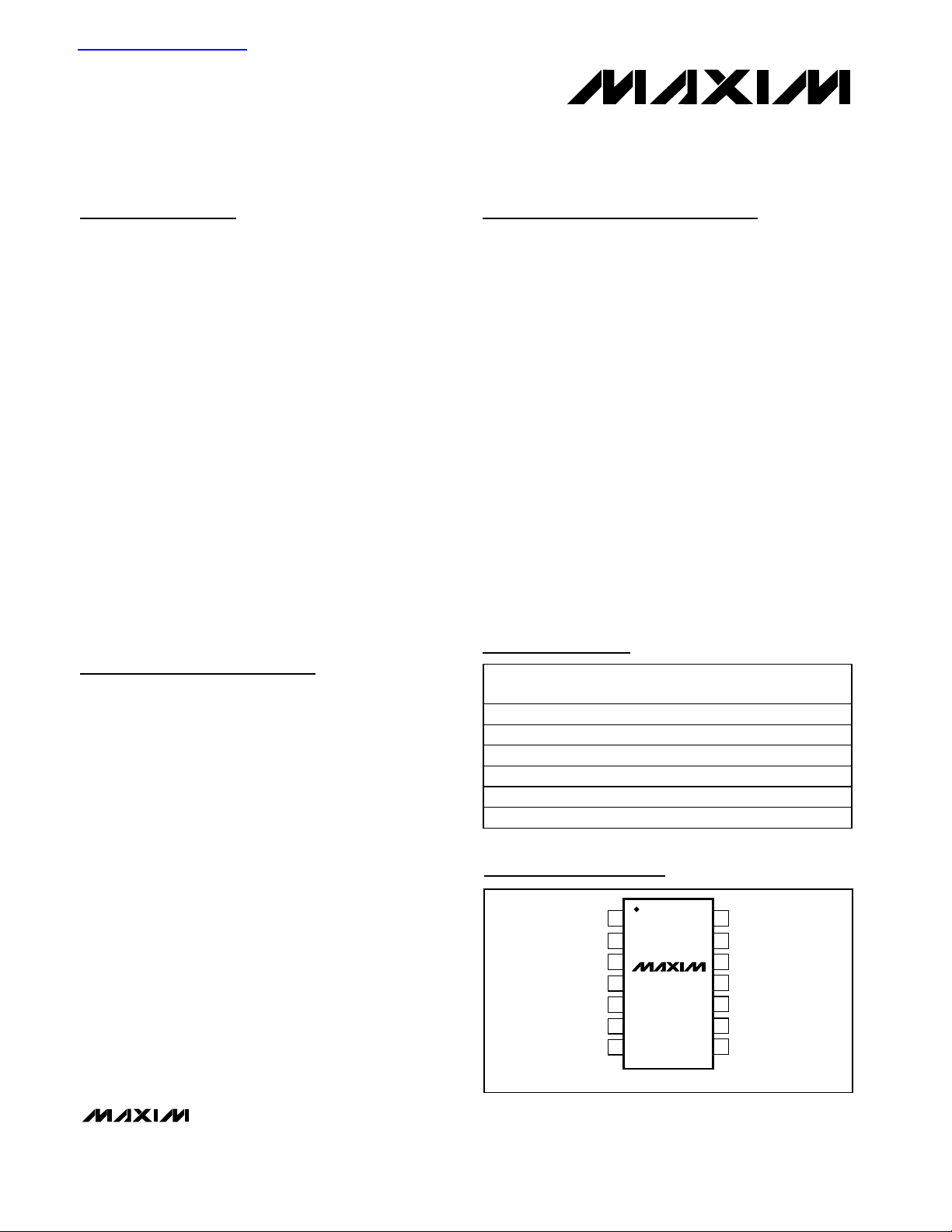
Ordering Information
(
)
Pin Configuration
I2C is a trademark of Philips Corp.
AutoShutdown is a trademark of Maxim Integrated Products, Inc.
*Future product—contact factory for availability.
查询MAX1069供应商
PART TEMP RANGE
MAX1069ACUD 0°C to +70°C 14 TSSOP ±1
MAX1069BCUD 0°C to +70°C 14 TSSOP ±2
MAX1069CCUD 0°C to +70°C 14 TSSOP ±3
MAX1069AEUD* -40°C to +85°C 14 TSSOP ±1
MAX1069BEUD* -40°C to +85°C 14 TSSOP ±2
MAX1069CEUD* -40°C to +85°C 14 TSSOP ±3
PINPACKAGE
INL
LSB
TOP VIEW
DGND
SCL
SDA
ADD1
ADD0
DV
1
2
3
4
5
6
7
DD
ADD3
14
REF
13
REFADJ
12
AGNDSADD2
MAX1069
TSSOP
11
10
AIN
9
AGND
8
AV
DD
Page 2
MAX1069
58.6ksps, 14-Bit, 2-Wire Serial ADC
in a 14-Pin TSSOP
2 _______________________________________________________________________________________
ABSOLUTE MAXIMUM RATINGS
Stresses beyond those listed under “Absolute Maximum Ratings” may cause permanent damage to the device. These are stress ratings only, and functional
operation of the device at these or any other conditions beyond those indicated in the operational sections of the specifications is not implied. Exposure to
absolute maximum rating conditions for extended periods may affect device reliability.
AV
DD
to AGND .........................................................-0.3V to +6V
DV
DD
to DGND.........................................................-0.3V to +6V
AGND to DGND.....................................................-0.3V to +0.3V
AGNDS to AGND...................................................-0.3V to +0.3V
AIN, REF, REFADJ to AGND....................-0.3V to (AV
DD
+ 0.3V)
SCL, SDA, ADD_ to DGND.......................................-0.3V to +6V
Maximum Current into Any Pin............................................50mA
Continuous Power Dissipation (T
A
= +70°C)
14-Pin TSSOP (derate 9.1mW/°C above +70°C) .........727mW
Operating Temperature Ranges:
MAX1069_CUD ..................................................0°C to +70°C
MAX1069_EUD ................................................-40°C to +85°C
Storage Temperature Range .............................-65°C to +150°C
Junction Temperature......................................................+150°C
Lead Temperature (soldering, 10s) .................................+300°C
ELECTRICAL CHARACTERISTICS
(AVDD= +4.75V to +5.25V, DVDD= +2.7V to +5.5V, f
SCL
= 1.7MHz (33% duty cycle), f
SAMPLE
= 58.6ksps, V
REF
= +4.096V, external ref-
erence applied to REF, REFADJ = AV
DD
, C
REF
= 10µF, TA= T
MIN
to T
MAX
, unless otherwise noted. Typical values are at TA= +25°C.)
DC ACCURACY (Note 1)
Resolution 14 Bits
Relative Accuracy
(Note 2)
Offset Error 25mV
Offset-Error Temperature
Coefficient
Gain Error (Note 3) ±0.25 ±0.5 %FSR
Gain Temperature Coefficient 0.1 ppm/°C
DYNAMIC PERFORMANCE (f
Signal-to-Noise Plus Distortion SINAD 81 84 dB
Total Harmonic Distortion THD Up to the 5th harmonic -99 -86 dB
Spurious-Free Dynamic Range SFDR 87 102 dB
Signal-to-Noise Ratio SNR 82 84 dB
Full-Power Bandwidth FPBW -3dB point 4 MHz
Full-Linear Bandwidth SINAD > 81dB 20 kHz
CONVERSION RATE (Figure 11)
Conversion Time
(SCL Stretched Low)
Throughput Rate (Note 4) f
Internal Clock Frequency f
Track/Hold Acquisition Time t
PARAMETER SYMBOL CONDITIONS MIN TYP MAX UNITS
INL
IN(sine wave)
t
CONV
SAMPLE
CLK
ACQ
= 1kHz, VIN = V
MAX1069A ±1
MAX1069B ±2
MAX1069C ±3
MAX1069A, no missing codes ±1
MAX1069B, no missing codes ±1Differential Nonlinearity DNL
MAX1069C, no missing codes ±1
Fast mode 7.1 7.5
High-speed mode 5.8 6
Fast mode 19
High-speed mode 58.6
(Note 5) 1100 ns
REF(P-P)
, f
SAMPLE
= 58.6ksps)
1.0 ppm/°C
4 MHz
LSB
LSB
µs
ksps
Page 3
MAX1069
58.6ksps, 14-Bit, 2-Wire Serial ADC
in a 14-Pin TSSOP
_______________________________________________________________________________________ 3
ELECTRICAL CHARACTERISTICS (continued)
(AVDD= +4.75V to +5.25V, DVDD= +2.7V to +5.5V, f
SCL
= 1.7MHz (33% duty cycle), f
SAMPLE
= 58.6ksps, V
REF
= +4.096V, external ref-
erence applied to REF, REFADJ = AV
DD
, C
REF
= 10µF, TA= T
MIN
to T
MAX
, unless otherwise noted. Typical values are at TA= +25°C.)
Aperture Delay
(Figure 11c) (Note 6)
Aperture Jitter
(Figure 11c)
PARAMETER SYMBOL CONDITIONS MIN TYP MAX UNITS
t
AD
t
AJ
ANALOG INPUT (AIN)
Input Voltage Range V
AIN
Input Leakage Current
Input Capacitance C
IN
INTERNAL REFERENCE (Bypass REFADJ with 0.1µF to AGND and REF with 10µF to AGND)
REF Output Voltage V
Reference Temperature
Coefficient
Reference Short-Circuit Current I
REF
TC
REF
REFSC
REFADJ Output Voltage 4.056 4.096 4.000 V
REFADJ Input Range For small adjustments, from 4.096V ±60 mV
EXTERNAL REFERENCE (REFADJ = AVDD)
REFADJ Buffer Disable Voltage
REFADJ Buffer Enable Voltage AV
Reference Input Voltage Range
REF Input Current I
REF
DIGITAL INPUTS/OUTPUTS (SCL, SDA)
Input High Voltage V
Input Low Voltage V
Input Hysteresis V
Input Current I
Input Capacitance C
Output Low Voltage V
IH
IL
HYST
IN
IN
OL
ADDRESS SELECT INPUTS (ADD3, ADD2, ADD1, ADD0)
Input High Voltage 0.7 × DV
Input Low Voltage 0.3 × DV
Input Hysteresis 0.1 × DV
Input Current ±10 µA
Input Capacitance 15 pF
Fast mode 50
High-speed mode 30
Fast mode 100
High-speed mode 100
0V
On/off-leakage current, V
no clock, f
SCL
= 0
= 0V or AVDD,
AIN
±0.01 ±10 µA
35 pF
4.056 4.096 4.136 V
TA = 0°C to +70°C ±20
TA = -40°C to +85°C ±35
10 4.136 mA
Pull REFADJ high to disable the internal
bandgap reference and reference buffer
AVDD - 0.1 V
DD
(Note 7) 1.0 AV
V
= +4.096V, VIN = V
REF
f
IN(sine wave)
V
REF
= 1kHz, f
= +4.096V, shutdown 0.1
REF(P-P)
SAMPLE
= 62.1ksps
0.7 × DV
27
DD
0.3 × DV
0.1 × DV
DD
±10 µA
15 pF
I
= 3mA 0.4 V
SINK
DD
DD
REF
ppm/°C
- 0.4 V
DD
DD
DD
ns
ps
V
V
µA
V
V
V
V
V
V
Page 4
MAX1069
58.6ksps, 14-Bit, 2-Wire Serial ADC
in a 14-Pin TSSOP
4 _______________________________________________________________________________________
ELECTRICAL CHARACTERISTICS (continued)
(AVDD= +4.75V to +5.25V, DVDD= +2.7V to +5.5V, f
SCL
= 1.7MHz (33% duty cycle), f
SAMPLE
= 58.6ksps, V
REF
= +4.096V, external ref-
erence applied to REF, REFADJ = AV
DD
, C
REF
= 10µF, TA= T
MIN
to T
MAX
, unless otherwise noted. Typical values are at TA= +25°C.)
PARAMETER SYM B O L CONDITIONS MIN TYP MAX UNITS
POWER REQUIREMENTS (AVDD, AGND, DVDD, DGND)
Analog Supply Voltage AV
Digital Supply Voltage DV
DD
DD
Analog Supply Current I
Digital Supply Current I
Power-Supply Rejection Ratio
TIMING CHARACTERISTICS FOR 2-WIRE FAST MODE (Figure 1a and Figure 2)
Serial Clock Frequency f
Bus Free Time Between a STOP
and a START Condition
Hold Time for Start Condition t
Low Period of the SCL Clock t
High Period of the SCL Clock t
Setup Time for a Repeated
START Condition (Sr)
Data Hold Time t
Data Setup Time t
Rise Time of Both SDA and SCL
Signals, Receiving
Fall Time of SDA Transmitting t
Setup Time for STOP Condition t
C ap aci ti ve Load for E ach Bus Li ne C
Pulse Width of Spike Suppressed t
AVDD
DVDD
PSRR AV
SCL
t
BUF
HD,STA
LOW
HIGH
t
SU,STA
HD,DAT
SU,DAT
t
R
F
SU,STO
B
SP
Inter nal r efer ence
( p ow er ed d ow n
b etw een conver si ons,
R/W = 0)
Internal reference
(always on, R/W = 1)
f
SAMPLE
f
SAMPLE
f
SAMPLE
Shutdown 0.4 5.0
f
SAMPLE
f
SAMPLE
f
SAMPLE
= 58.6ksps 1.8 2.5
= 10ksps 0.7
= 1ksps 40
= 58.6ksps 1.8 2.5
= 10ksps 1.4
= 1ksps 1.1 mA
Shutdown 0.4 5 µA
f
= 58.6ksps 0.90 1.8
SAMPLE
f
= 10ksps 0.36
External reference
(REFADJ = AV
DD
SAMPLE
)
f
= 1ksps 40
SAMPLE
Shutdown 0.4 5
f
f
f
= 58.6ksps 260 400
SAMPLE
= 10ksps 65
SAMPLE
= 1ksps 6
SAMPLE
Shutdown 0.2 5
= 5V ±5%, full-scale input (Note 8) 2 6 LSB/V
DD
(Note 9) 0 900 ns
(Note 10)
(Note 10)
4.75 5.25 V
2.7 5.5 V
400 kHz
1.3 µs
0.6 µs
1.3 µs
0.6 µs
0.6 µs
100 ns
20 +
0.1C
20 +
0.1C
B
B
300 ns
300 ns
0.6 µs
400 pF
mA
µA
mA
mA
µA
µA
50 ns
Page 5
MAX1069
58.6ksps, 14-Bit, 2-Wire Serial ADC
in a 14-Pin TSSOP
_______________________________________________________________________________________ 5
Note 1: DC accuracy is tested at AVDD= +5.0V and DVDD= +3.0V. Performance at power-supply tolerance limits is guaranteed
by power-supply rejection test.
Note 2: Relative accuracy is the deviation of the analog value at any code from its theoretical value after the full-scale range and
offset have been calibrated.
Note 3: Offset nullified.
Note 4: One sample is achieved every 18 clocks in continuous conversion mode.
Note 5: The track/hold acquisition time is two SCL cycles as illustrated in Figure 11.
Note 6: A filter on SDA and SCL delays the sampling instant and suppresses noise spikes less than 10ns in high-speed mode and
50ns in fast mode.
Note 7: ADC performance is limited by the converter’s noise floor, typically 480µV
P-P
.
Note 8:
ELECTRICAL CHARACTERISTICS (continued)
(AVDD= +4.75V to +5.25V, DVDD= +2.7V to +5.5V, f
SCL
= 1.7MHz (33% duty cycle), f
SAMPLE
= 58.6ksps, V
REF
= +4.096V, external ref-
erence applied to REF, REFADJ = AV
DD
, C
REF
= 10µF, TA= T
MIN
to T
MAX
, unless otherwise noted. Typical values are at TA= +25°C.)
TIMING CHARACTERISTICS FOR 2-WIRE HIGH-SPEED MODE (Figure 1b and Figure 2)
Serial Clock Frequency f
Hold Time, (Repeated) Start
Condition
Low Period of the SCL Clock t
High Period of the SCL Clock t
Setup Time for a Repeated
START Condition
Data Hold Time t
Data Setup Time t
Rise Time of SCL Signal
(Current Source Enabled)
Rise Time of SCL Signal After
Acknowledge Bit
Fall Time of SCL Signal
Rise Time of SDA Signal
Fall Time of SDA Signal
Setup Time for STOP Condition t
C ap aci ti ve Load for E ach Bus Li ne C
Pulse Width of Spike Suppressed t
PARAMETER SYM B O L CONDITIONS MIN TYP MAX UNITS
t
HD,STA
t
HD,DAT
SU,DAT
SU,STO
SCLH
LOW
HIGH
SU,STA
t
RCL
t
RCL1
t
FCL
t
RDA
t
FDA
B
SP
(Note 11) 1.7 MHz
(Note 9) 0 150 ns
(Note 10) 10 80 ns
(Note 10) 20 160 ns
(Note 10) 20 80 ns
(Note 10) 20 160 ns
(Note 10) 20 160 ns
160 ns
320 ns
120 ns
160 ns
10 ns
160 ns
400 pF
10 ns
f
SAMPLE
t2
ACQ
PSRR
1 clocks
8
=+
=×
1
f
SCL
V (5.25V) - V (4.75V)
[]
FS FS
=
f
SCL
5.25V - 4.75V
-1
t
C
ONV
N
2
×
V
REF
where N is the number of bits ( ).14
Page 6
MAX1069
58.6ksps, 14-Bit, 2-Wire Serial ADC
in a 14-Pin TSSOP
6 _______________________________________________________________________________________
Note 9: A master device must provide a data hold time for SDA (referred to VILof SCL) in order to bridge the undefined region of
SCL’s falling edge (see Figure 1).
Note 10: C
B
= total capacitance of one bus line in pF. tRand tFmeasured between 0.3 ✕DVDDand 0.7 ✕DVDD.
Note 11: f
SCL
must meet the minimum clock low time plus the rise/fall times.
ELECTRICAL CHARACTERISTICS (continued)
(AVDD= +4.75V to +5.25V, DVDD= +2.7V to +5.5V, f
SCL
= 1.7MHz (33% duty cycle), f
SAMPLE
= 58.6ksps, V
REF
= +4.096V, external ref-
erence applied to REF, REFADJ = AV
DD
, C
REF
= 10µF, TA= T
MIN
to T
MAX
, unless otherwise noted. Typical values are at TA= +25°C.)
Figure 1. I2C Serial Interface Timing
Figure 2. Load Circuit
2
A. F/S-MODE I
SDA
SCL
B. HS-MODE I
SDA
C SERIAL INTERFACE TIMING
t
SU,DAT
t
LOW
t
t
HD,STA
S Sr A
2
C SERIAL INTERFACE TIMING
t
SU,DAT
t
LOW
HIGH
t
R
t
HD,DAT
t
F
t
HD,DAT
t
SU,STA
t
SU,STA
t
HD,STA
t
HD,STA
t
SU,STO
t
RDA
t
SU,STO
t
R
PS
t
F
t
BUF
t
BUF
t
FDA
SCL
t
HD,STA
t
RCL
S Sr A
PARAMETERS ARE MEASURED FROM 30% TO 70%.
t
HIGH
V
DD
DIGITAL
I/O
IOL = 3mA
I
= 0mA
OH
t
FCL
400pF
t
RCL1
P
HS-MODE
V
OUT
S
F/S-MODE
Page 7
MAX1069
58.6ksps, 14-Bit, 2-Wire Serial ADC
in a 14-Pin TSSOP
_______________________________________________________________________________________ 7
Typical Operating Characteristics
(DVDD= +3.0V, AVDD= +5.0V, f
SCL
= 1.7MHz (33% duty cycle), f
SAMPLE
= 58.6ksps, V
REF
= +4.096V, external reference applied to
REF, REFADJ = AV
DD
, C
REF
= 10µF, TA= +25°C, unless otherwise noted.)
ANALOG SUPPLY CURRENT vs. ANALOG
SUPPLY VOLTAGE (INTERNAL REFERENCE)
1.75
DVDD = 3V
1.73
1.71
(mA)
1.69
AVDD
I
1.67
1.65
1.63
4.75 5.25
AV
(V)
DD
DIGITAL SUPPLY CURRENT
vs. DIGITAL SUPPLY VOLTAGE
280
AVDD = 5V
260
240
(µA)
DVDD
I
220
200
180
160
140
120
100
TA = +85°C
2.7 5.5
ANALOG SUPPLY CURRENT vs. ANALOG
SUPPLY VOLTAGE (EXTERNAL REFERENCE)
830
DVDD = 3V
820
MAX1069 toc01
810
800
(µA)
AVDD
I
TA = +85°C
TA = +70°C
TA = +25°C
TA = 0°C
TA = -40°C
5.155.054.954.85
DVDD (V)
790
780
770
760
MAX1069 toc04
TA = -40°C
5.14.73.9 4.33.53.1
AV
(V)
DD
TA = +85°C
TA = +70°C
TA = +25°C
TA = 0°C
TA = -40°C
5.155.054.954.854.75 5.25
350
300
250
200
(nA)
DVDD
150
I
100
50
ANALOG SHUTDOWN CURRENT
vs. ANALOG SUPPLY VOLTAGE
700
DVDD = 3V
= 0
f
SAMPLE
600
MAX1069 toc02
R/W = 0
500
400
(nA)
AVDD
300
I
200
100
0
4.75 5.25
AV
(V)
DD
DIGITAL SHUTDOWN CURRENT
vs. DIGITAL SUPPLY VOLTAGE
AVDD = 5V
= 0
f
SAMPLE
R/W = 0
TA = +70°C
0
2.7 5.5
TA = 0°C
TA = +25°C
DV
TA = -40°C
4.3 4.7 5.13.93.53.1
(V)
DD
TA = +85°C
TA = +85°C
TA = +70°C
TA = +25°C
TA = 0°C
TA = -40°C
MAX1069 toc03
5.155.054.954.85
MAX1069 toc05
OFFSET ERROR
vs. TEMPERATURE
800
600
400
200
0
-200
OFFSET ERROR (µV)
-400
-600
-800
-40 85
TEMPERATURE (°C)
0.008
MAX1069 toc06
6035-15 10
0.006
0.004
0.002
0
-0.002
GAIN ERROR (%FSR)
-0.004
-0.006
-0.008
-40 85
GAIN ERROR
vs. TEMPERATURE
6035-15 10
TEMPERATURE (°C)
MAX1069 toc07
Page 8
MAX1069
58.6ksps, 14-Bit, 2-Wire Serial ADC
in a 14-Pin TSSOP
8 _______________________________________________________________________________________
Typical Operating Characteristics (continued)
(DVDD= +3.0V, AVDD= +5.0V, f
SCL
= 1.7MHz (33% duty cycle), f
SAMPLE
= 58.6ksps, V
REF
= +4.096V, external reference applied to
REF, REFADJ = AV
DD
, C
REF
= 10µF, TA= +25°C, unless otherwise noted.)
SUPPLY CURRENT vs. CONVERSION RATE
(HIGH-SPEED MODE, INTERNAL REFERENCE)
MAX1069 toc08
CONVERSION RATE (ksps)
SUPPLY CURRENT (µA)
605030 402010
200
400
600
800
1000
1200
1400
1600
1800
2000
0
070
INTERNAL REFERENCE, f
SCL
= 1.7MHz
I
AVDD
, R/W = 1
I
AVDD
, R/W = 0
I
DVDD
, R/W = 1 OR 0
100
200
300
400
500
600
700
800
900
0
SUPPLY CURRENT vs. CONVERSION RATE
(HIGH-SPEED MODE, EXTERNAL REFERENCE)
MAX1069 toc09
CONVERSION RATE (ksps)
SUPPLY CURRENT (µA)
605030 402010070
EXTERNAL REFERENCE, f
SCL
= 1.7MHz
I
DVDD
, R/W = 1 OR 0
I
AVDD
, R/W = 1 OR 0
SUPPLY CURRENT vs. CONVERSION RATE
(FAST MODE, INTERNAL REFERENCE)
MAX1069 toc10
CONVERSION RATE (ksps)
SUPPLY CURRENT (µA)
2015105
200
400
600
800
1000
1200
1400
1600
1800
0
025
INTERNAL REFERENCE, f
SCL
= 400kHz
I
AVDD
, R/W = 1
I
AVDD
, R/W = 0
I
DVDD
, R/W = 1 OR 0
100
200
300
400
500
600
0
SUPPLY CURRENT vs. CONVERSION RATE
(FAST MODE, EXTERNAL REFERENCE)
MAX1069 toc11
CONVERSION RATE (ksps)
SUPPLY CURRENT (µA)
2015105025
EXTERNAL REFERENCE, f
SCL
= 400kHz
I
DVDD
, R/W = 1 OR 0
I
AVDD
, R/W = 1 OR 0
Page 9

MAX1069
58.6ksps, 14-Bit, 2-Wire Serial ADC
in a 14-Pin TSSOP
_______________________________________________________________________________________ 9
Typical Operating Characteristics (continued)
(DVDD= +3.0V, AVDD= +5.0V, f
SCL
= 1.7MHz (33% duty cycle), f
SAMPLE
= 58.6ksps, V
REF
= +4.096V, external reference applied to
REF, REFADJ = AV
DD
, C
REF
= 10µF, TA= +25°C, unless otherwise noted.)
INTERNAL +4.096V REFERENCE VOLTAGE
vs. ANALOG SUPPLY VOLTAGE
4.100
DVDD = 3V
4.095
4.090
(V)
REF
V
4.085
4.080
4.075
4.75 5.25
EXTERNAL REFERENCE CURRENT
vs. EXTERNAL REFERENCE VOLTAGE
35
AIN = AGNDS
30
25
20
(µA)
REF
I
15
10
5
f
SCL
58.6ksps
= 1.7MHz
TA = +85°C
TA = +70°C
TA = +25°C
TA = 0°C
TA = -40°C
AVDD (V)
19ksps
f
SCL
5.155.054.954.85
= 400kHz
MAX1069 toc12
MAX1069 toc14
4.20
4.15
4.10
(V)
4.05
REF
V
4.00
3.95
3.90
06
EXTERNAL REFERENCE CURRENT AND
REFERENCE VOLTAGE vs. V
30
AIN = AGNDS
20
10
(µA)
0
REFADJ
I
-10
-20
INTERNAL REFERENCE VOLTAGE
vs. REF LOAD
f
= 0
INTERNAL REFERENCE MODE
LOAD APPLIED TO REF
I
(mA)
REF
I
REFADJ
V
REF
SCL
54321
REFADJ
MAX1069 toc15
MAX1069 toc13
4.25
4.20
4.15
4.10
4.05
4.00
(V)
REF
V
0
V
(V)
REF
5432106
-30
3.95 4.25
V
REFADJ
4.204.154.104.054.00
(V)
3.95
Page 10

MAX1069
58.6ksps, 14-Bit, 2-Wire Serial ADC
in a 14-Pin TSSOP
10 ______________________________________________________________________________________
Typical Operating Characteristics (continued)
(DVDD= +3.0V, AVDD= +5.0V, f
SCL
= 1.7MHz (33% duty cycle), f
SAMPLE
= 58.6ksps, V
REF
= +4.096V, external reference applied to
REF, REFADJ = AV
DD
, C
REF
= 10µF, TA= +25°C, unless otherwise noted.)
SIGNAL-TO-NOISE RATIO
vs. FREQUENCY
MAX1069 toc16
FREQUENCY (kHz)
SNR (dB)
120
110
100
90
80
70
60
50
40
30
20
10
0
1 10 100
SPURIOUS-FREE DYNAMIC RANGE
vs. FREQUENCY
MAX1069 toc17
FREQUENCY (kHz)
SFDR (dB)
120
110
100
90
80
70
60
50
40
30
20
10
0
1 10 100
DIFFERENTIAL NONLINEARITY
vs. DIGITAL OUTPUT CODE
MAX1069 toc18
DIGITAL OUTPUT CODE
DNL (LSB)
1228881924096
-0.8
-0.6
-0.4
-0.2
0
0.2
0.4
0.6
0.8
1.0
-1.0
0 16384
TOTAL HARMONIC DISTORTION
vs. FREQUENCY
MAX1069 toc19
FREQUENCY (kHz)
THD (dB)
0
-10
-20
-30
-40
-50
-60
-70
-80
-90
-100
-110
-120
1 10 100
SINAD vs. FREQUENCY
MAX1069 toc20
FREQUENCY (kHz)
SINAD (dB)
120
110
100
90
80
70
60
50
40
30
20
10
0
1 10 100
INTEGRAL NONLINEARITY
vs. DIGITAL OUTPUT CODE
MAX1069 toc21
DIGITAL OUTPUT CODE
INL (LSB)
1228881924096
-0.8
-0.6
-0.4
-0.2
0
0.2
0.4
0.6
0.8
1.0
-1.0
0 16384
FFT
MAX1069 toc22
FREQUENCY (kHz)
MAGNITUDE (dB)
23.4417.5611.725.86
-120
-100
-80
-60
-40
-20
0
-140
0 29.30
f
SAMPLE
= 58.6ksps
f
IN(SINE WAVE)
= 1kHz
V
IN
= V
REF(P-P)
Page 11
Detailed Description
The MAX1069 analog-to-digital converter (ADC) uses
successive-approximation conversion (SAR) techniques and on-chip track-and-hold (T/H) circuitry to
capture and convert an analog signal to a serial 14-bit
digital output.
The MAX1069 performs a unipolar conversion on its
single analog input using its internal 4MHz clock. The
full-scale analog input range is determined by the internal reference or by an externally applied reference voltage ranging from 1V to AVDD.
The flexible 2-wire serial interface provides easy connection to microcontrollers (µCs) and supports data
rates up to 1.7MHz. Figure 3 shows the simplified func-
tional diagram for the MAX1069 and Figure 4 shows the
typical application circuit.
Power Supply
To maintain a low-noise environment, the MAX1069
provides separate analog and digital power-supply
inputs. The analog circuitry requires a +5V supply and
consumes only 900µA at sampling rates up to
58.6ksps. The digital supply voltage accepts voltages
from +2.7V to +5.5V to ensure compatibility with lowvoltage ASICs. The MAX1069 wakes up in shutdown
mode when power is applied irrespective of the AV
DD
and DVDDsequence.
Analog Input and Track/Hold
The MAX1069 analog input contains a track-and-hold
(T/H) capacitor, T/H switches, comparator, and a
switched capacitor digital-to-analog converter (DAC)
(Figure 5).
As shown in Figure 11c, the MAX1069 acquisition period is the two clock cycles prior to the conversion period. The T/H switches are normally in the hold position.
During the acquisition period the T/H switches are in
the track position and C
T/H
charges to the analog input
signal. Before a conversion begins, the T/H switches
move to the hold position retaining the charge on C
T/H
as a sample of the analog input signal.
During the conversion interval, the switched capacitive
DAC adjusts to restore the comparator input voltage to
zero within the limits of 14-bit resolution. This is equivalent to transferring a charge of 35pF × (V
AIN
- V
AGNDS
)
from C
T/H
to the binary-weighted capacitive DAC,
MAX1069
58.6ksps, 14-Bit, 2-Wire Serial ADC
in a 14-Pin TSSOP
______________________________________________________________________________________ 11
Pin Description
PIN NAME FUNCTION
1 DGND Digital Ground
2 SCL Clock Input
3 SDA Data Input/Output
4 ADD2 Address Select Input 2
5 ADD1 Address Select Input 1
6 ADD0 Address Select Input 0
7DVDDDigital Power Input. Bypass to DGND with a 0.1µF capacitor.
8AVDDAnalog Power Input. Bypass to AGND with a 0.1µF capacitor.
9 AGND Analog Ground
10 AIN Analog Input
11 AGNDS Analog Signal Ground. Negative reference for analog input. Connect to AGND.
12 REFADJ
13 REF
14 ADD3 Address Select Input 3
Internal Reference Output and Reference Buffer Input. Bypass to AGND with a 0.1µF capacitor.
Connect REFADJ to AV
Reference Buffer Output and External Reference Input. Bypass to AGND with a 10µF capacitor
when using the internal reference.
to disable the internal bandgap reference and reference-buffer amplifier.
DD
Page 12

MAX1069
forming a digital representation of the analog input signal. During the conversion period, the MAX1069 holds
SCL low (clock stretching).
The time required for the T/H to acquire an input signal
is a function of the analog input source impedance. If
the input signal source impedance is high, lengthen the
acquisition time by reducing f
SCL
. The MAX1069 pro-
vides two SCL cycles (t
ACQ
), in which the track-andhold capacitance must acquire a charge representing
the input signal. Minimize the input source impedance
(R
SOURCE
) to allow the track-and-hold capacitance to
charge within the allotted time. R
SOURCE
should be
less than 12.9kΩ for f
SCL
= 400kHz and less than 2.4kΩ
58.6ksps, 14-Bit, 2-Wire Serial ADC
in a 14-Pin TSSOP
12 ______________________________________________________________________________________
Figure 3. MAX1069 Simplified Functional Diagram
Figure 4. Typical Application Circuit
CONTROL
LOGIC
AV
AGND
8
DD
9
4MHz
INTERNAL
OSCILLATOR
10
AIN
11
AGNDS
+4.096V
REFERENCE
12
REFADJ
13
REF
5.0V
8
0.1µF
13
10µF
12
0.1µF
T/H
AV
DD
REF
REFADJ
5kΩ
MAX1069
DV
ADD0
ADD1
ADD2
SDA
SCL
DD
IN
AV = 1.0
7
6
5
4
3
2
CLOCK
SAR
ADC
REF
3.0V
0.1µF
OUT
R
P
OUTPUT SHIFT
REGISTER
MAX1069
R
P
V
SDA
SCL
6
ADD0
5
ADD1
4
ADD2
14
ADD3
3
SDA
2
SCL
7
DV
DD
1
DGND
µC
DD
ANALOG
SOURCE
10
AIN
11
AGNDS
AGND DGND
91
ADD3
14
2
I
C ADDRESS IS 0110111
V
SS
Page 13

for f
SCL
= 1.7MHz. R
SOURCE
is calculated with the fol-
lowing equation:
where R
SOURCE
is the analog input source impedance,
f
SCL
is the maximum system SCL frequency, N is 14
(the number of bits of resolution), C
IN
is 35pF (the sum
of C
T/H
and input stray capacitance), and R
IN
is 800Ω
(the T/H switch resistances).
To improve the input-signal bandwidth under AC
conditions, drive AIN with a wideband buffer
(>4MHz) that can drive the ADC’s input capacitance
and settle quickly (see the Input Buffer section).
An RC filter at AIN reduces the input track-and-hold
switching transient by providing charge for C
T/H
.
Analog Input Bandwidth
The MAX1069 features input-tracking circuitry with a
4MHz small-signal bandwidth. The 4MHz input bandwidth makes it possible to digitize high-speed transient
events and measure periodic signals with bandwidths
exceeding the ADC’s sampling rate by using undersampling techniques. Use anti-alias filtering to avoid
high-frequency signals being aliased into the frequency
band of interest.
Analog Input Range and Protection
Internal ESD (electrostatic discharge) protection diodes
clamp AIN, REF, and REFADJ to AV
DD
and
AGNDS/AGND (Figure 6). These diodes allow the ana-
log inputs to swing from (AGND - 0.3V) to (AVDD+
0.3V) without causing damage to the device. For accurate conversions, the inputs must not go more than
50mV beyond their rails.
If the analog inputs exceed 300mV beyond their
rails, limit the current to 2mA.
Internal Clock
The MAX1069 contains an internal 4MHz oscillator that
drives the SAR conversion clock. During conversion, SCL
is held low (clock stretching). An internal register stores
data when the conversion is in progress. When the
MAX1069 releases SCL, the master reads the conversion
results at any clock rate up to 1.7MHz (Figure 11).
Digital Interface
The MAX1069 features an I2C-compatible, 2-wire serial
interface consisting of a bidirectional serial data line
(SDA) and a serial clock line (SCL). SDA and SCL facilitate bidirectional communication between the
MAX1069 and the master at rates up to 1.7MHz. The
master (typically a microcontroller) initiates data transfer on the bus and generates SCL.
SDA and SCL require pullup resistors (500Ω or greater,
Figure 4). Optional resistors (24Ω) in series with SDA
and SCL protect the device inputs from high-voltage
spikes on the bus lines. Series resistors also minimize
crosstalk and undershoot of the bus signals.
Bit Transfer
One data bit is transferred during each SCL clock
cycle. Nine clock cycles are required to transfer the
data into or out of the MAX1069. The data on SDA must
remain stable during the high period of the SCL clock
pulse as changes in SDA while SCL is high are control
signals (see the START and STOP Conditions section).
Both SDA and SCL idle high.
START and STOP Conditions
The master initiates a transmission with a START condition (S), a high-to-low transition on SDA with SCL high.
The master terminates a transmission with a STOP condition (P), a low-to-high transition on SDA while SCL is
high (Figure 7). The STOP condition frees the bus and
places all devices in F/S mode (see the Bus Timing
section). Use a repeated START condition (Sr) in place
MAX1069
58.6ksps, 14-Bit, 2-Wire Serial ADC
in a 14-Pin TSSOP
______________________________________________________________________________________ 13
Figure 5. Equivalent Input Circuit
Figure 6. Internal Protection Diodes
R
SOURCE
≤
fIn
SCL
2
N
(
22)C
×××
−
IN
R
IN
*R
SOURCE
ANALOG
SIGNAL
SOURCE
AIN
HOLD
TRACK
TRACK
C
T/H
HOLD
TRACK
HOLD
REF
MAX1069
CAPACITIVE
DAC
AV
DD
AIN
REF
MAX1069
AGNDS
*MINIMIZE R
CHARGE TO THE ANALOG SIGNAL SOURCE VOLTAGE WITHIN THE ALLOTTED TIME (t
TO ALLOW THE TRACK-AND-HOLD CAPACITANCE (C
SOURCE
) TO
T/H
ACQ
REFADJ
AGNDS
AGND
).
Page 14

MAX1069
of a STOP condition to leave the bus active and in its
current timing mode (see the HS-Mode section).
Acknowledge Bits
Successful data transfers are acknowledged with an
acknowledge bit (A) or a not-acknowledge bit (A). Both
the master and the MAX1069 (slave) generate acknowledge bits. To generate an acknowledge, the receiving
device must pull SDA low before the rising edge of the
acknowledge-related clock pulse (ninth pulse) and
keep it low during the high period of the clock pulse
(Figure 8). To generate a not acknowledge, the receiver
allows SDA to be pulled high before the rising edge of
the acknowledge-related clock pulse and leaves it high
during the high period of the clock pulse.
Monitoring the acknowledge bits allows for detection of
unsuccessful data transfers. An unsuccessful data
transfer happens if a receiving device is busy or if a
system fault has occurred. In the event of an unsuccessful data transfer, the master should reattempt communication at a later time.
Slave Address
A master initiates communication with a slave device by
issuing a START condition followed by a slave address
byte. As shown in Figure 9, the slave address byte consists of 7 address bits and a read/write bit (R/W). When
idle, the MAX1069 continuously waits for a START condition followed by its slave address. When the
MAX1069 recognizes its slave address, it acquires the
analog input signal and prepares for conversion. The
first three bits (MSBs) of the slave address have been
factory programmed and are always 011. Connecting
ADD3–ADD0 to DVDDor DGND, programs the last four
bits (LSBs) of the slave address high or low.
Since the MAX1069 does not require setup or configuration, the least significant bit (LSB) of the address byte
(R/W) controls power-down. In external reference mode
(REFADJ = AVDD), R/W is a don’t care. In internal reference mode, setting R/W = 1 places the device in normal operation and setting R/W = 0 powers down the
internal reference following the conversion (see the
Internal Reference Shutdown section).
After receiving the address, the MAX1069 (slave)
issues an acknowledge by pulling SDA low for one
clock cycle.
Bus Timing
At power-up, the MAX1069 bus timing defaults to fast
mode (F/S-mode), allowing conversion rates up to
19ksps. The MAX1069 must operate in high-speed
mode (HS-mode) to achieve conversion rates up to
58.6ksps. Figure 1 shows the bus timing for the
MAX1069 2-wire interface.
HS-Mode
At power-up, the MAX1069 bus timing is set for F/Smode. The master selects HS-mode by addressing all
devices on the bus with the HS-mode master code 0000
1XXX (X = don’t care). After successfully receiving the
HS-mode master code, the MAX1069 issues a not
acknowledge allowing SDA to be pulled high for one
58.6ksps, 14-Bit, 2-Wire Serial ADC
in a 14-Pin TSSOP
14 ______________________________________________________________________________________
Figure 8. Acknowledge Bits
Figure 7. START and STOP Conditions
SPSr
SDA
SCL
SDA
SCL
S
12 8 9
NOT ACKNOWLEDGE
ACKNOWLEDGE
Page 15
clock cycle (Figure 10). After the not acknowledge, the
MAX1069 is in HS-mode. The master must then send a
repeated START followed by a slave address to initiate
HS-mode communication. If the master generates a
STOP condition, the MAX1069 returns to F/S-mode.
Data Byte (Read Cycle)
Initiate a read cycle to begin a conversion. A read
cycle begins with the master issuing a START condition
followed by seven address bits and a read bit (R/W).
The standard I2C-compatible interface requires that
R/W = 1 to read from a device, however, since the
MAX1069 does not require setup or configuration, the
read mode is inherent and R/W controls power-down
(see the Internal Reference Shutdown section). If the
address byte is successfully received, the MAX1069
(slave) issues an acknowledge and begins conversion.
As seen in Figure 11, the MAX1069 holds SCL low during conversion. When the conversion is complete, SCL
is released and the master can clock data out of the
device. The most significant byte of the conversion is
available first and contains D13 to D6. The least significant byte contains D5 to D0 plus two trailing sub bits
S1 and S0. Data can be continuously converted as long
as the master acknowledges the conversion results.
Issuing a not acknowledge frees the bus allowing the
master to generate a STOP or repeated START.
Applications Information
Power-On Reset
When power is first applied, internal power-on reset circuitry activates the MAX1069 in shutdown. When the
internal reference is used, allow 12ms for the reference
to settle when C
REF
= 10µF and C
REFADJ
= 0.1µF.
Automatic Shutdown
The MAX1069 automatic shutdown reduces the supply
current to less than 0.6µA between conversions. The
MAX1069 I2C-compatible interface is always active.
When the MAX1069 receives a valid slave address the
device powers up. The device is then powered down
again when the conversion is complete. The automatic
shutdown function does not change with internal or
external reference. When the internal reference is chosen, the internal reference remains active between conversions unless internal reference shutdown is requested
(see the Internal Reference Shutdown section).
Internal Reference Shutdown
The R/W bit of the slave address controls the MAX1069
internal reference shutdown. In external reference
mode (REFADJ = AVDD), R/W is a don’t care. In internal
reference mode, setting R/W = 1 places the device in
normal operation and setting R/W = 0 prepares the
internal reference for shutdown.
MAX1069
58.6ksps, 14-Bit, 2-Wire Serial ADC
in a 14-Pin TSSOP
______________________________________________________________________________________ 15
Figure 10. F/S-Mode to HS-Mode Transfer
Figure 9. MAX1069 Slave Address Byte
SDA
S
110
ADD3 ADD2 ADD1 ADD0
R/W
ACKNOWLEDGE
A
SCL
S
SDA
123
000
123
01XXX
F/S-MODE
894567
Sr
A
894567
HS-MODE
Page 16
MAX1069
If the internal reference is used and R/W = 0, shutdown
occurs when the master issues a not-acknowledge bit
while reading the conversion results. The internal reference and internal reference buffer are disabled during
shutdown, reducing the analog supply current to less
than 1µA.
A dummy conversion is required to power up the internal reference. The MAX1069 internal reference begins
powering up from shutdown on the 9th falling edge of a
valid address byte. Allow 12ms for the internal reference to settle before obtaining valid conversion results.
Reference Voltage
The MAX1069 provides an internal or accepts an external reference voltage. The ADC input range is from
V
AGNDS
to V
REF
(see the Transfer Function section).
58.6ksps, 14-Bit, 2-Wire Serial ADC
in a 14-Pin TSSOP
16 ______________________________________________________________________________________
Figure 11. Read Cycle
S1SLAVE ADDRESS
71
R
NUMBER OF BITS
P OR Sr
1
1
8
RESULT #1 A
18
RESULT #1 A
1
8
RESULT A
18
RESULT A
1
CLOCK STRETCH
t
CONV
t
ACQ
A
8
RESULT #2 A
1
CLOCK STRETCH
t
CONV
t
ACQ
NUMBER OF BITS
89567
BIT3 BIT2 BIT1 BIT0 A
CLOCK STRETCH
t
AD
t
ACQ
t
AJ
SCL
SDA
123
D10D12 D11
t
CONV
8
RESULT #2 A
1
NUMBER OF BITS
P OR Sr
1A18
RESULT #N A
18
RESULT #N
CLOCK STRETCH
t
CONV
t
ACQ
(MOST SIGNIFICANT BYTE) (LEAST SIGNIFICANT BYTE)
(MOST SIGNIFICANT BYTE) (LEAST SIGNIFICANT BYTE)
(LEAST SIGNIFICANT BYTE)
(MOST SIGNIFICANT BYTE)
(MOST SIGNIFICANT BYTE) (LEAST SIGNIFICANT BYTE)
ANALOG INPUT
TRACK AND HOLD
TRACKHOLD HOLD
B. CONTINUOUS CONVERSIONS
A. SINGLE CONVERSION
SLAVE TO MASTER
MASTER TO SLAVE
C. ACQUISITION DETAIL
D13
4
RS1SLAVE ADDRESS A
711
CLOCK STRETCH
t
ACQ
t
CONV
Page 17
Internal Reference
The MAX1069 contains an internal 4.096V bandgap reference. This bandgap reference is connected to
REFADJ through a 5kΩ resistor. Bypass REFADJ with a
0.1µF capacitor to AGND. The MAX1069 reference
buffer has a unity gain to provide +4.096V at REF.
Bypass REF with a 10µF capacitor to AGND when the
internal reference is used (Figure 12).
The internal reference is adjustable to ±1.5% using the
Figure 13 circuit.
External Reference
For external reference operation, disable the internal
reference by connecting REFADJ to AVDD. During conversion, an external reference at REF must deliver up to
100µA of DC load current and have an output impedance of less than 10Ω.
For optimal performance, buffer the reference through
an op amp and bypass REF with a 10µF capacitor.
Consider the MAX1069’s equivalent input noise
(80µV
RMS
) when choosing a reference.
Transfer Function
The MAX1069 has a standard unipolar transfer function
with a valid analog input voltage range from V
AGNDS
to
V
REF
. Output data coding is binary with 1LSB =
(V
REF
/2N) where ‘N’ is the number of bits (14). Code
transitions occur halfway between successive-integer
LSB values. Figure 14 shows the MAX1069 input/output
(I/O) transfer function.
Input Buffer
Most applications require an input buffer amplifier to
achieve 14-bit accuracy. If the input signal is multiplexed, the input channel should be switched immediately after acquisition, rather than near the end of or
MAX1069
58.6ksps, 14-Bit, 2-Wire Serial ADC
in a 14-Pin TSSOP
______________________________________________________________________________________ 17
Figure 12. Internal Reference
Figure 13. Adjusting the Internal Reference
13
SAR
ADC
MAX1069
4.096V
BANDGAP
REFERENCE
REF
A
1
4.096V
= 1.0
V
5kΩ
REF
10µF
REFADJ
12
0.1µF
AGNDDGND
9
4.096V
BANDGAP
REFERENCE
MAX1069
SAR
ADC
REF
1
A
V
= 1.0
4.096V
5kΩ
8
AV
DD
0.1µF
13
REF
10µF
REFADJ
12
AGNDDGND
9
68kΩ
0.1µF
5.0V
100kΩ
POTENTIOMETER
150kΩ
Page 18
MAX1069
after a conversion. This allows more time for the input
buffer amplifier to respond to a large step-change in
input signal. The input amplifier must have a high
enough slew rate to complete the required output voltage change before the beginning of the acquisition
time. At the beginning of acquisition, the internal sampling capacitor array connects to AIN (the amplifier output), causing some output disturbance.
Ensure that the sampled voltage has settled to within
the required limits before the end of the acquisition
time. If the frequency of interest is low, AIN can be
bypassed with a large enough capacitor to charge the
internal sampling capacitor with very little ripple.
However, for AC use, AIN must be driven by a wideband buffer (at least 4MHz), which must be stable with
the ADC’s capacitive load (in parallel with any AIN
bypass capacitor used) and also settle quickly. Refer to
Maxim’s website at www.maxim-ic.com for application
notes on how to choose the optimum buffer amplifier for
your ADC application.
Layout, Grounding, and Bypassing
Careful printed circuit (PC) layout is essential for the
best system performance. Boards should have separate analog and digital ground planes and ensure that
digital and analog signals are separated from each
other. Do not run analog and digital (especially clock)
lines parallel to one another, or digital lines underneath
the device package.
Figure 4 shows the recommended system ground con-
nections. Establish an analog ground point at AGND
and a digital ground point at DGND. Connect all analog
grounds to the star analog ground. Connect the digital
grounds to the star digital ground. Connect the digital
ground plane to the analog ground plane at one point.
For lowest-noise operation, make the ground return to
the star ground’s power-supply low impedance and
make it as short as possible.
High-frequency noise in the AVDDpower supply
degrades the ADC’s high-speed comparator performance. Bypass AVDDto AGND with a 0.1µF ceramic
surface-mount capacitor. Make bypass capacitor connections as short as possible. If the power supply is
very noisy, connect a 10Ω resistor in series with AV
DD
and a 4.7µF capacitor from AVDDto AGND to create a
lowpass RC filter.
Definitions
Integral Nonlinearity
Integral nonlinearity (INL) is the deviation of the values
on an actual transfer function from a straight line. This
straight line can be either a best-straight-line fit or a line
drawn between the end points of the transfer function
once offset and gain errors have been nullified. The
MAX1069 INL is measured using the endpoint method.
Differential Nonlinearity
Differential nonlinearity (DNL) is the difference between
an actual step width and the ideal value of 1LSB. A
DNL error specification of less than 1LSB guarantees
no missing codes and a monotonic transfer function.
Aperture Jitter
Aperture jitter (tAJ) is the sample-to-sample variation in
the time between the samples (Figure 11).
Aperture Delay
Aperture delay (tAD) is the time from the falling edge of
SCL to the instant when an actual sample is taken
(Figure 11).
Signal-to-Noise Ratio
For a waveform perfectly reconstructed from digital samples, signal-to-noise ratio (SNR) is the ratio of full-scale
analog input (RMS value) to the RMS quantization error
(residual error). The ideal, theoretical minimum analogto-digital noise is caused by quantization error only and
results directly from the ADC’s resolution (N bits):
SNR = ((6.02
✕
N) + 1.76)dB
In reality, noise sources besides quantization noise
exist, including thermal noise, reference noise, clock jitter, etc. Therefore, SNR is computed by taking the ratio
of the RMS signal to the RMS noise, which includes all
spectral components minus the fundamental, the first
five harmonics, and the DC offset.
58.6ksps, 14-Bit, 2-Wire Serial ADC
in a 14-Pin TSSOP
18 ______________________________________________________________________________________
Figure 14. Unipolar Transfer Function
AGNDS
INPUT VOLTAGE (LSB)
BINARY OUTPUT CODE (LSB)
012 3
16384
1LSB =
V
REF
1638316381
0...000
0...001
0...010
0...011
1...111
1...110
1...101
1...100
V
REF
V
REF
Page 19

Signal-to-Noise Plus Distortion
Signal-to-noise plus distortion (SINAD) is the ratio of the
fundamental input frequency’s RMS amplitude to RMS
equivalent of all other ADC output signals.
Effective Number of Bits
Effective number of bits (ENOB) indicates the global
accuracy of an ADC at a specific input frequency and
sampling rate. An ideal ADC’s error consists of quantization noise only. With an input range equal to the
ADC’s full-scale range, calculate the ENOB as follows:
Total Harmonic Distortion
Total harmonic distortion (THD) is the RMS sum ratio of
the input signal’s first five harmonics to the fundamental
itself, expressed as:
where V1is the fundamental amplitude, and V2through
V
5
are the amplitudes of the 2nd- through 5th-order
harmonics.
Spurious-Free Dynamic Range
Spurious-free dynamic range (SFDR) is the ratio of RMS
amplitude of the fundamental (maximum signal component) to the RMS value of the next-largest distortion
component.
Chip Information
TRANSISTOR COUNT: 18,269
PROCESS: BiCMOS
MAX1069
58.6ksps, 14-Bit, 2-Wire Serial ADC
in a 14-Pin TSSOP
______________________________________________________________________________________ 19
SINAD db( ) log
=
20
Signal
×
Noise
RMS
RMS
E
NOB
SINAD - 1.76
=
602.
=
THD
20
×
232
V+V+V+V
2
log
2
4
V
1
2
5
Page 20
MAX1069
58.6ksps, 14-Bit, 2-Wire Serial ADC
in a 14-Pin TSSOP
Maxim cannot assume responsibility for use of any circuitry other than circuitry entirely embodied in a Maxim product. No circuit patent licenses are
implied. Maxim reserves the right to change the circuitry and specifications without notice at any time.
20 ____________________Maxim Integrated Products, 120 San Gabriel Drive, Sunnyvale, CA 94086 408-737-7600
© 2002 Maxim Integrated Products Printed USA is a registered trademark of Maxim Integrated Products.
Package Information
(The package drawing(s) in this data sheet may not reflect the most current specifications. For the latest package outline information,
go to www.maxim-ic.com/packages.)
TSSOP4.40mm.EPS
 Loading...