

General Description
The MAX1067/MAX1068 low-power, multichannel, 14bit analog-to-digital converters (ADCs) feature a successive-approximation ADC, integrated +4.096V
reference, a reference buffer, an internal oscillator,
automatic power-down, and a high-speed SPI™/
QSPI™/MICROWIRE™-compatible interface. The
MAX1067/MAX1068 operate with a single +5V analog
supply and feature a separate digital supply, allowing
direct interfacing with +2.7V to +5.5V digital logic.
The MAX1067/MAX1068 consume only 2.9mA (AVDD=
DVDD= +5V) at 200ksps when using an external reference. AutoShutdown™ reduces the supply current to
145µA at 10ksps and to less than 10µA at reduced sampling rates.
The MAX1067 includes a 4-channel input multiplexer, and
the MAX1068 accepts up to eight analog inputs.
In addition, digital signal processor (DSP)-initiated conversions are simplified with the DSP frame-sync input and
output featured in the MAX1068. The MAX1068 includes a
data-bit transfer input to select between 8-bit-wide or 16bit-wide data-transfer modes. Both devices feature a scan
mode that converts each channel sequentially or one
channel continuously.
Excellent dynamic performance and low power, combined with ease of use and an integrated reference,
make the MAX1067/MAX1068 ideal for control and dataacquisition operations or for other applications with
demanding power consumption and space requirements. The MAX1067 is available in a 16-pin QSOP
package, and the MAX1068 is available in a 24-pin
QSOP package. Both devices are guaranteed over the
commercial (0°C to +70°C) and extended (-40°C to
+85°C) temperature ranges. Use the MAX1168 evaluation kit to evaluate the MAX1068.
Applications
Motor Control
Industrial Process Control
Industrial I/O Modules
Data-Acquisition Systems
Thermocouple Measurements
Accelerometer Measurements
Features
♦ 14-Bit Resolution, ±0.5 LSB INL and
±1 LSB DNL (max)
♦ +5V Single-Supply Operation
♦ Adjustable Logic Level (+2.7V to +5.25V)
♦ Input Voltage Range: 0 to V
REF
♦ Internal (+4.096V) or External (+3.8V to AVDD)
Reference
♦ Internal Track/Hold, 4MHz Input Bandwidth
♦ Internal or External Clock
♦ SPI/QSPI/MICROWIRE-Compatible Serial
Interface, MAX1068 Performs DSP-Initiated
Conversions
♦ 8-Bit-Wide or 16-Bit-Wide Data-Transfer Mode
(MAX1068 Only)
♦ 4-Channel (MAX1067) or 8-Channel (MAX1068)
Input Mux
Scan Mode Sequentially Converts Multiple
Channels or One Channel Continuously
♦ Low Power
2.9mA at 200ksps
1.45mA at 100ksps
145µA at 10ksps
0.6µA in Full Power-Down Mode
♦ Small Package Size
16-Pin QSOP (MAX1067)
24-Pin QSOP (MAX1068)
MAX1067/MAX1068
Multichannel, 14-Bit, 200ksps Analog-to-Digital
Converters
________________________________________________________________ Maxim Integrated Products 1
Ordering Information
19-2955; Rev 0; 8/03
For pricing, delivery, and ordering information, please contact Maxim/Dallas Direct! at
1-888-629-4642, or visit Maxim’s website at www.maxim-ic.com.
Ordering Information continued at end of data sheet.
SPI/QSPI are trademarks of Motorola, Inc.
MICROWIRE is a trademark of National Semiconductor Corp.
AutoShutdown is a trademark of Maxim Integrated Products, Inc.
Pin Configurations appear at end of data sheet.
查询MAX1067AEEE供应商
PART TEMP RANGE
MAX1067ACEE 0°C to +70°C 16 QSOP ±0.5
MAX1067BCEE 0°C to +70°C 16 QSOP ±1
MAX1067CCEE 0°C to +70°C 16 QSOP ±2
MAX1067AEEE -40°C to +85°C 16 QSOP ±0.5
MAX1067BEEE -40°C to +85°C 16 QSOP ±1
MAX1067CEEE -40°C to +85°C 16 QSOP ±2
PINPACKAGE
(LSB)
INL
MAX1067/MAX1068
Multichannel, 14-Bit, 200ksps Analog-to-Digital
Converters
2 _______________________________________________________________________________________
ABSOLUTE MAXIMUM RATINGS
Stresses beyond those listed under “Absolute Maximum Ratings” may cause permanent damage to the device. These are stress ratings only, and functional
operation of the device at these or any other conditions beyond those indicated in the operational sections of the specifications is not implied. Exposure to
absolute maximum rating conditions for extended periods may affect device reliability.
AVDDto AGND .........................................................-0.3V to +6V
DV
DD
to DGND.........................................................-0.3V to +6V
DGND to AGND.....................................................-0.3V to +0.3V
AIN_, REF, REFCAP to AGND..................-0.3V to (AV
DD
+ 0.3V)
SCLK, CS, DSEL, DSPR, DIN to DGND ...................-0.3V to +6V
DOUT, DSPX, EOC to DGND...................-0.3V to (DV
DD
+ 0.3V)
Maximum Current into Any Pin............................................50mA
Continuous Power Dissipation (T
A
= +70°C)
16-Pin QSOP (derate 8.3mW/°C above +70°C)...........667mW
24-Pin QSOP (derate 9.5mW/°C above +70°C)...........762mW
Operating Temperature Ranges
MAX106_ _ CE_ ..................................................0°C to +70°C
MAX106_ _ EE_ ...............................................-40°C to +85°C
Maximum Junction Temperature .....................................+150°C
Storage Temperature Range .............................-65°C to +150°C
Lead Temperature (soldering, 10s) .................................+300°C
ELECTRICAL CHARACTERISTICS
(AVDD= DVDD= +4.75V to +5.25V, f
SCLK
= 4.8MHz external clock (50% duty cycle), 24 clocks/conversion (200ksps), external V
REF
= +4.096V, TA= T
MIN
to T
MAX
, unless otherwise noted. Typical values are at TA= +25°C.)
DC ACCURACY (Note 1)
Resolution 14 Bits
Relative Accuracy (Note 2) INL
Differential Nonlinearity DNL
Transition Noise RMS noise
Offset Error ±0.1 ±10 mV
Gain Error (Note 3) ±0.01 ±0.2 %FSR
Offset Drift 1 ppm/°C
Gain Drift (Note 3) ±1.2 ppm/°C
DYNAMIC SPECIFICATIONS (1kHz sine wave, 4.096V
Signal-to-Noise Plus Distortion SINAD 81 84 dB
Signal-to-Noise Ratio SNR 82 84 dB
Total Harmonic Distortion THD -98 -86 dB
Spurious-Free Dynamic Range SFDR 87 99 dB
Full-Power Bandwidth -3dB point 4 MHz
Full-Linear Bandwidth SINAD > 81dB 10 kHz
Channel-to-Channel Isolation (Note 4) 85 dB
CONVERSION RATE
Conversion Time t
PARAMETER SYMBOL CONDITIONS MIN TYP MAX UNITS
MAX106_A ±0.5 ±1
MAX106_B ±1.0 ±2
MAX106_C ±1.5 ±3
MAX106_A ±1
MAX106_B
MAX106_C
External reference 0.33
Internal reference 0.35
CONV
No missing codes
over temperature
) (Note 1)
P-P
Internal clock, no data transfer,
single conversion (Note 5)
External clock 3.75
5.52 7.07
+1.5
-1.0
+1.5
-1.0
LSB
LSB
LSB
RMS
µs
MAX1067/MAX1068
Multichannel, 14-Bit, 200ksps Analog-to-Digital
Converters
_______________________________________________________________________________________ 3
ELECTRICAL CHARACTERISTICS (continued)
(AVDD= DVDD= +4.75V to +5.25V, f
SCLK
= 4.8MHz external clock (50% duty cycle), 24 clocks/conversion (200ksps), external V
REF
= +4.096V, TA= T
MIN
to T
MAX
, unless otherwise noted. Typical values are at TA= +25°C.)
Acquisition Time t
Serial Clock Frequency f
Internal Clock Frequency f
Aperture Delay t
Aperture Jitter t
Sample Rate (Note 7) f
Duty Cycle 45 55 %
ANALOG INPUT (AIN_)
Input Range V
Input Capacitance C
EXTERNAL REFERENCE
Input Voltage Range V
Input Current I
INTERNAL REFERENCE
Reference Voltage V
Reference Short-Circuit Current I
Reference Temperature
Coefficient
Reference Wake-Up Time t
PARAMETER SYMBOL CONDITIONS MIN TYP MAX UNITS
ACQ
SCLK
INTCLK
AD
AJ
AIN
AIN
REF
REF
REFIN
REFSC
RWAKEVREF
(Note 6) 729 ns
External clock, data transfer and conversion 0.1 4.8
External clock, data transfer only 9
Internal clock 3.2 4.0 MHz
15 ns
<50 ps
8-bit-wide data-transfer mode 4.17 200.00
16-bit-wide data-transfer mode 3.125 150.000
Internal clock, single conversion, 8-bit-wide
data-transfer mode
Internal clock, single conversion, 16-bit-
S
wide data-transfer mode
Internal clock, scan mode, 8-bit-wide datatransfer mode (four conversions)
External clock, scan mode, 16-bit-wide
data-transfer mode (four conversions)
_0V
_45pF
3.8 AV
V
_ = 0 110
AIN
SCLK idle 0.1
CS = DVDD, SCLK idle 0.1
4.056 4.096 4.136 V
= 0 5 ms
89
68
103
82
REF
DD
13 mA
±25 ppm/°C
MHz
ksps
V
V
µA
MAX1067/MAX1068
Multichannel, 14-Bit, 200ksps Analog-to-Digital
Converters
4 _______________________________________________________________________________________
ELECTRICAL CHARACTERISTICS (continued)
(AVDD= DVDD= +4.75V to +5.25V, f
SCLK
= 4.8MHz external clock (50% duty cycle), 24 clocks/conversion (200ksps), external V
REF
= +4.096V, TA= T
MIN
to T
MAX
, unless otherwise noted. Typical values are at TA= +25°C.)
DIGITAL INPUTS (SCLK, CS, DSEL, DSPR, DIN) (DVDD = +2.7V to +5.25V)
Input High Voltage V
Input Low Voltage V
Input Leakage Current I
Input Hysteresis V
Input Capacitance C
DIGITAL OUTPUT (DOUT, DSPX, EOC) (DVDD = +2.7V to +5.25V)
Output High Voltage V
Output Low Voltage V
Tri-State Output Leakage Current I
Tri-State Output Capacitance C
POWER SUPPLIES
Analog Supply AV
Digital Supply DV
Analog Supply Current (Note 8) I
Digital Supply Current I
Power-Down Supply Current
PARAMETER SYMBOL CONDITIONS MIN TYP MAX UNITS
0.7 ×
DV
DD
0.3 ×
DV
±0.1 ±1 µA
0.2 V
15 pF
DV
-
DD
0.4
±0.1 ±10 µA
15 pF
4.75 5.25 V
2.70 5.25 V
1.01
0.43
HYST
AVDD
DVDD
I
AVDD
I
DVDD
IH
IL
IN
IN
OH
OL
L
OUT
DD
DD
Digital inputs = 0 to DV
+
I
I
I
CS = DV
CS = DV
200ksps
100ksps
10ksps
1ksps
DOUT =
all zeros
CS = DVDD,
SCLK = 0,
DIN = 0,
DSPR = DV
= 0.5mA
SOURCE
= 10mA, DVDD = +4.75V to +5.25V 0.8
SINK
= 1.6mA, DVDD = +2.7V to +5.25V 0.4
SINK
DD
DD
DD
External reference 2.0 2.9
Internal reference 2.9 3.8
External reference 1.0
Internal reference 2.0
External reference 0.1
Internal reference 1.1
External reference 0.01
Internal reference 1.01
200ksps 0.87 1.3
100ksps 0.45
10ksps 0.045
1ksps 0.005
Internal reference and
reference buffer on
between conversions
Internal reference on,
DD
reference buffer off
between conversions
DD
V
V
V
V
mA
mA
mA
MAX1067/MAX1068
Multichannel, 14-Bit, 200ksps Analog-to-Digital
Converters
_______________________________________________________________________________________ 5
ELECTRICAL CHARACTERISTICS (continued)
(AVDD= DVDD= +4.75V to +5.25V, f
SCLK
= 4.8MHz external clock (50% duty cycle), 24 clocks/conversion (200ksps), external V
REF
= +4.096V, TA= T
MIN
to T
MAX
, unless otherwise noted. Typical values are at TA= +25°C.)
TIMING CHARACTERISTICS (Figures 1, 2, 8, and 16)
(AVDD= DVDD= +4.75V to +5.25V, f
SCLK
= 4.8MHz external clock (50% duty cycle), 24 clocks/conversion (200ksps), external V
REF
= +4.096V, TA= T
MIN
to T
MAX
, unless otherwise noted. Typical values are at TA= +25°C.)
Shutdown Supply Current
Power-Supply Rejection Ratio PSRR
PARAMETER SYMBOL CONDITIONS MIN TYP MAX UNITS
I
+
AVDD
I
DVDD
CS = DVDD, SCLK = 0, DIN = 0,
DSPR = DV
= DVDD = 4.75V to 5.25V, full-scale
AV
DD
input (Note 9)
, full power-down
DD
Acquisition Time t
SCLK to DOUT Valid t
CS Fall to DOUT Enable t
CS Rise to DOUT Disable t
CS Pulse Width t
CS to SCLK Setup t
CS to SCLK Hold t
SCLK High Pulse Width t
SCLK Low Pulse Width t
SCLK Period t
DIN to SCLK Setup t
DIN to SCLK Hold t
CS Falling to DSPR Rising t
DSPR to SCLK Falling Setup t
DSPR to SCLK Falling Hold t
PARAMETER SYMBOL CONDITIONS MIN TYP MAX UNITS
ACQ
DO
DV
TR
CSW
CSS
CSH
CH
CL
CP
DS
DH
DF
FSS
FSH
External clock (Note 6) 729 ns
C
= 30pF 50 ns
DOUT
C
= 30pF 80 ns
DOUT
C
= 30pF 80 ns
DOUT
SCLK rise
SCLK fall (DSP)
SCLK rise
SCLK fall (DSP)
Duty cycle 45% to 55%
Duty cycle 45% to 55%
SCLK rise
SCLK fall (DSP)
SCLK rise
SCLK fall (DSP)
100 ns
100 ns
Conversion 93
Data transfer 50
Conversion 93
Data transfer 50
209 ns
50 ns
100 ns
100 ns
0.6
63 dB
0ns
0ns
0ns
10
µA
ns
ns
MAX1067/MAX1068
Multichannel, 14-Bit, 200ksps Analog-to-Digital
Converters
6 _______________________________________________________________________________________
TIMING CHARACTERISTICS (Figures 1, 2, 8, and 16)
(AVDD= +4.75V to +5.25V, DVDD= +2.7V to +5.25V, f
SCLK
= 4.8MHz external clock (50% duty cycle), 24 clocks/conversion
(200ksps), external V
REF
= +4.096V, TA= T
MIN
to T
MAX
, unless otherwise noted. Typical values are at TA= +25°C.)
Note 1: AVDD= DVDD= +5.0V.
Note 2: Relative accuracy is the deviation of the analog value at any code from its theoretical value after full-scale range has been
calibrated.
Note 3: Offset and reference errors nulled.
Note 4: DC voltage applied to on channel, and a full-scale 1kHz sine wave applied to off channels.
Note 5: Conversion time is measured from the rising edge of the 8th external SCLK pulse to EOC transition minus t
ACQ
in 8-bit data-
transfer mode.
Note 6: See Figures 10 and 17.
Note 7: f
SCLK
= 4.8MHz, f
INTCLK
= 4.0MHz. Sample rate is calculated with the formula fs= n1(n2 / f
SCLK
+ n3 / f
INTCLK
)-1where: n
1
= number of scans, n2= number of SCLK cycles, and n3= number of internal clock cycles (see Figures 11–14).
Note 8: Internal reference and buffer are left on between conversions.
Note 9: Defined as the change in the positive full scale caused by a ±5% variation in the nominal supply voltage.
Acquisition Time t
SCLK to DOUT Valid t
CS Fall to DOUT Enable t
CS Rise to DOUT Disable t
CS Pulse Width t
CS to SCLK Setup t
CS to SCLK Hold t
SCLK High Pulse Width t
SCLK Low Pulse Width t
SCLK Period t
DIN to SCLK Setup t
DIN to SCLK Hold t
CS Falling to DSPR Rising t
DSPR to SCLK Falling Setup t
DSPR to SCLK Falling Hold t
PARAMETER SYMBOL CONDITIONS MIN TYP MAX UNITS
ACQ
DO
DV
TR
CSW
CSS
CSH
CH
CL
CP
DS
DH
DF
FSS
FSH
External clock (Note 6) 729 ns
C
DOUT
C
DOUT
C
DOUT
SCLK rise
SCLK fall (DSP)
SCLK rise
SCLK fall (DSP)
Duty cycle 45% to 55%
Duty cycle 45% to 55%
SCLK rise
SCLK fall (DSP)
SCLK rise
SCLK fall (DSP)
= 30pF 100 ns
= 30pF 100 ns
= 30pF 80 ns
100 ns
100 ns
0ns
Conversion 93
Data transfer 93
Conversion 93
Data transfer 93
209 ns
100 ns
0ns
100 ns
100 ns
0ns
ns
ns
MAX1067/MAX1068
Multichannel, 14-Bit, 200ksps Analog-to-Digital
Converters
_______________________________________________________________________________________ 7
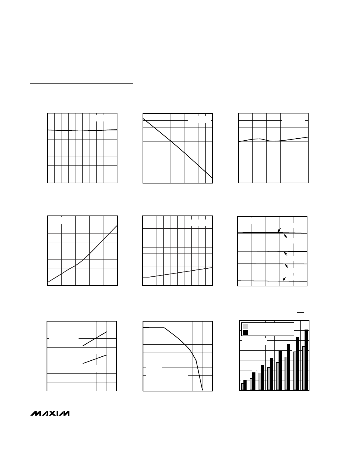
Typical Operating Characteristics
(AVDD= DVDD= +5V, f
SCLK
= 4.8MHz, C
DOUT
= 30pF, external V
REF
= +4.096V, TA= +25°C, unless otherwise noted.)
INL vs. CODE
1.0
0.8
0.6
0.4
0.2
0
INL (LSB)
-0.2
-0.4
-0.6
-0.8
-1.0
0 81924096 12,288 16,384
CODE
SINAD vs. FREQUENCY
90
80
70
60
50
40
SINAD (dB)
30
20
10
0
0.1 100
FREQUENCY (kHz)
f
SAMPLE
= 200kbps
101
1.0
0.8
0.6
MAX1067/68 toc01
0.4
0.2
0
DNL (LSB)
-0.2
-0.4
-0.6
-0.8
-1.0
120
100
MAX1067/68 toc04
80
60
SFDR (dB)
40
20
0
DNL vs. CODE
0 81924096 12,288 16,384
CODE
SFDR vs. FREQUENCY
f
= 200ksps
SAMPLE
0.1 100
FREQUENCY (kHz)
101
MAX1067/68 toc02
MAX1067/68 toc05
20
FFT AT f
0
-20
-40
-60
-80
AMPLITUDE (dB)
-100
-120
-140
-160
0608020 40 100
= 1kHz
AIN
FREQUENCY (kHz)
THD vs. FREQUENCY
0
f
= 200kbps
SAMPLE
-20
-40
-60
THD (dB)
-80
-100
-120
0.1 100
FREQUENCY (kHz)
101
MAX1067/68 toc03
MAX1067/68 toc06
SUPPLY CURRENT vs. CONVERSION RATE
(EXTERNAL CLOCK)
3.0
DVDD = AVDD = +5V
= ALL ZEROS
D
OUT
2.5
EXTERNAL CLOCK
SPI MODE
2.0
1.5
1.0
SUPPLY CURRENT (mA)
0.5
0
-0.5
0200
I
, INT REF
AVDD
I
, EXT REF
AVDD
I
DVDD
CONVERSION RATE (ksps)
MAX1067/68 toc07
(mA)
AVDD
I
18016014012010080604020
vs. ANALOG SUPPLY VOLTAGE
(INTERNAL REFERENCE)
2.95
DVDD = +5V
= 200ksps
f
S
2.90
2.85
2.80
2.75
2.70
4.75 5.25
ANALOG SUPPLY CURRENT
TA = +85°C
AVDD (V)
TA = +70°C
TA = +25°C
TA = 0°C
TA = -40°C
5.155.054.954.85
MAX1067/68 toc08
ANALOG SUPPLY CURRENT
vs. ANALOG SUPPLY VOLTAGE
(EXTERNAL REFERENCE)
2.00
DVDD = +5V
= 200ksps
f
S
1.95
1.90
(mA)
AVDD
I
1.85
1.80
1.75
4.75 5.25
TA = +85°C
TA = +70°C
TA = +25°C
TA = -40°C
AVDD (V)
MAX1067/68 toc09
TA = 0°C
5.155.054.954.85
MAX1067/MAX1068
Multichannel, 14-Bit, 200ksps Analog-to-Digital
Converters
8 _______________________________________________________________________________________
Typical Operating Characteristics (continued)
(AVDD= DVDD= +5V, f
SCLK
= 4.8MHz, C
DOUT
= 30pF, external V
REF
= +4.096V, TA= +25°C, unless otherwise noted.)
DIGITAL SUPPLY CURRENT
vs. DIGITAL SUPPLY VOLTAGE
2.6
AVDD = +5V
= 0
V
IL
2.2
= 200ksps
f
S
1.8
(mA)
1.4
DVDD
I
1.0
0.6
DOUT = 1010...1010
DOUT = 0000...0000
0.58
0.57
MAX1067/68 toc10
0.56
(µA)
0.55
DVDD
I
0.54
0.53
POWER-DOWN SUPPLY CURRENT
vs. AV
DD
(INTERNAL REFERENCE)
DVDD = +5V
I
DVDD
SUPPLY VOLTAGE
MAX1067/68 toc11
I
AVDD
1.04
1.03
1.02
1.01
1.00
0.99
(mA)
AVDD
I
(µA)
DVDD
I
POWER-DOWN SUPPLY CURRENT
SUPPLY VOLTAGE
vs. DV
DD
(INTERNAL REFERENCE)
0.7
DVDD = +5VAVDD = +5V
0.6
0.5
0.4
0.3
0.2
I
DVDD
MAX1067/68 toc12
I
AVDD
1.03
1.02
1.01
1.00
(mA)
AVDD
I
0.2
2.70 5.25
DVDD (V)
4.744.233.723.21
0.52
4.75 5.25
SHUTDOWN SUPPLY CURRENT
SUPPLY VOLTAGE
vs. AV
DD
(EXTERNAL REFERENCE)
0.58
DVDD = +5V
0.57
0.56
(µA)
I
I
0.55
DVDD
DVDD
0.54
0.53
0.52
4.75 5.25
AVDD (V)
MAX1067/68 toc13
I
AVDD
5.155.054.954.85
POWER-DOWN SUPPLY CURRENT
vs. TEMPERATURE (INTERNAL REFERENCE)
0.58
DVDD = AVDD = +5V
0.57
0.56
(µA)
0.55
DVDD
I
0.54
0.53
I
DVDD
MAX1067/68 toc15
I
AVDD
0.54
0.50
0.46
0.42
0.38
0.34
0.30
1.04
1.03
1.02
1.01
1.00
0.99
AVDD (V)
(nA)
AVDD
I
(mA)
AVDD
I
5.155.054.954.85
0.98
0.1
2.70 5.25
SHUTDOWN SUPPLY CURRENT
vs. DV
SUPPLY VOLTAGE
DD
(EXTERNAL REFERENCE)
0.7
DVDD = +5VAVDD = +5V
0.6
0.5
(µA)
0.4
DVDD
I
0.3
I
0.2
0.1
DVDD
2.70 5.25
DVDD (V)
SHUTDOWN SUPPLY CURRENT
vs. TEMPERATURE (EXTERNAL REFERENCE)
0.58
DVDD = AVDD = +5V
0.57
0.56
(µA)
0.55
DVDD
I
0.54
0.53
I
AVDD
I
DVDD
MAX1067/68 toc14
I
AVDD
4.744.233.723.21
MAX1067/68 toc16
DVDD (V)
0.45
0.43
0.41
0.39
0.37
0.43
0.42
0.41
0.40
0.39
0.38
0.37
(nA)
AVDD
I
(nA)
AVDD
I
4.744.233.723.21
0.99
0.52
-40 85
TEMPERATURE (°C)
603510-15
0.98
0.52
-40 85
TEMPERATURE (°C)
603510-15
0.35
OFFSET ERROR vs. SUPPLY VOLTAGE
MAX1067/68 toc17
AVDD (V)
OFFSET ERROR (µV)
5.154.85 5.054.95
-150
-100
-50
0
50
100
150
200
-200
4.75 5.25
V
REF
= +4.096V
GAIN ERROR vs. SUPPLY VOLTAGE
MAX1067/68 toc18
AVDD (V)
GAIN ERROR (%FSR)
5.154.85 5.054.95
-0.025
-0.020
-0.015
-0.010
-0.005
0
0.005
0.010
0.015
0.020
-0.030
4.75 5.25
V
REF
= +4.096V
MAX1067/MAX1068
Multichannel, 14-Bit, 200ksps Analog-to-Digital
Converters
_______________________________________________________________________________________ 9
Typical Operating Characteristics (continued)
(AVDD= DVDD= +5V, f
SCLK
= 4.8MHz, C
DOUT
= 30pF, external V
REF
= +4.096V, TA= +25°C, unless otherwise noted.)
GAIN ERROR vs. TEMPERATURE
0.015
V
= +4.096V
REF
0.010
0.005
0
-0.005
-0.010
GAIN ERROR (%FSR)
-0.015
-0.020
-0.025
-40 85
TEMPERATURE (°C)
603510-15
0
-10
-20
MAX1067/68 toc20
-30
-40
-50
-60
ISOLATION (dB)
-70
-80
-90
-100
-110
CHANNEL-TO-CHANNEL ISOLATION
0100
OFFSET ERROR vs. TEMPERATURE
500
400
300
200
100
0
-100
OFFSET ERROR (µV)
-200
-300
-400
-500
-40 85
INTERNAL +4.096V REFERENCE VOLTAGE
vs. FREQUENCY
FREQUENCY (kHz)
V
REF
= +4.096V
908060 7020 30 40 5010
MAX1067/68 toc21
(V)
V
4.104
4.100
4.096
REF
4.092
4.088
vs. ANALOG SUPPLY VOLTAGE
DVDD = +5V
4.75 5.25
TEMPERATURE (°C)
AVDD (V)
V
= +4.096V
REF
TA = +85°C
TA = +70°C
TA = +25°C
TA = 0°C
TA = -40°C
5.155.054.954.85
MAX1067/68 toc19
603510-15
MAX1067/68 toc22
EXTERNAL REFERENCE INPUT CURRENT
vs. EXTERNAL REFERENCE VOLTAGE
160
V
= 0
AIN
140
120
100
(µA)
REF
I
= 4.8MHz
f
SCLK
= DV
AV
DD
DD
80
60
40
20
0
199ksps, EXTERNAL CLOCK
87.19ksps, INTERNAL CLOCK
2.0 5.5
INTERNAL CLOCK CONVERSION TIME
(8th RISING SCLK TO FALLING EOC)
70
8-BIT DATA-TRANSFER MODE
60
16-BIT DATA-TRANSFER MODE
50
f
= 4.8MHz
SCLK
40
(ms)
CONV
t
30
20
10
0
17
12
10
6
1
NUMBER OF SCAN-MODE CONVERSIONS
31
24
22
17
46
39
38
33
28
= +5V
V
INTERNAL REFERENCE VOLTAGE
vs. REF LOAD
4.5
4.0
3.5
MAX1067/68 toc23
3.0
(V)
2.5
REF
V
2.0
1.5
f
= 0
SCLK
1.0
INTERNAL REFERENCE MODE
5.04.52.5 3.0 3.5 4.0
(V)
REF
LOAD APPLIED TO REF
0.5
= 1µF
C
REF
0
014
(mA)
I
REF
MAX1067/68 toc24
12106 842
60
53
MAX1067/68 toc25
44
8765432
MAX1067/MAX1068
Multichannel, 14-Bit, 200ksps Analog-to-Digital
Converters
10 ______________________________________________________________________________________
Pin Description
PIN
MAX1067 MAX1068
1 3 DOUT
2 4 SCLK
35DIN
46EOC
5 7 AIN0 Analog Input 0
6 8 AIN1 Analog Input 1
NAME FUNCTION
Serial Data Output. Data changes state on SCLK’s falling edge in SPI/QSPI/MICROWIRE
mode and on SCLK’s rising edge in DSP mode (MAX1068 only). DOUT is high impedance
when CS is high.
Serial Clock Input. SCLK drives the conversion process in external clock mode and clocks
data out.
Serial Data Input. Use DIN to communicate with the command/configuration/control register.
In SPI/QSPI/MICROWIRE mode, the rising edge of SCLK clocks in data at DIN. In DSP
mode, the falling edge of SCLK clocks in data at DIN.
End-of-Conversion Output. In internal clock mode, a logic low at EOC signals the end of a
conversion with the result available at DOUT. In external clock mode, EOC remains high.
7 9 AIN2 Analog Input 2
8 10 AIN3 Analog Input 3
9 15 REF
10 16 REFCAP
11 17 AGND Analog Ground. Connect to pin 18 (MAX1068) or pin 12 (MAX1067).
Reference Voltage Input/Output. V
a 10µF capacitor. Bypass with a 1µF (min) capacitor when using the internal reference.
Refer ence Byp ass C ap aci tor C onnecti on. Byp ass to AG N D w i th a 0.1µF cap aci tor w hen usi ng
i nter nal r efer ence. Inter nal r efer ence and b uffer shut d ow n i n exter nal r efer ence m od e.
sets the analog voltage range. Bypass to AGND with
REF
12 18 AGND Primary Analog Ground (Star Ground). Power return for AVDD.
13 19 AV
14 20 CS
15 21 DGND Digital Ground
16 22 DV
— 1 DSPR
— 2 DSEL
— 11 AIN4 Analog Input 4
— 12 AIN5 Analog Input 5
Analog Supply Voltage. Bypass to AGND with a 0.1µF capacitor.
DD
Active-Low Chip-Select Input. Forcing CS high places the MAX1067/MAX1068 in shutdown
with a typical supply current of 0.6µA. In SPI/QSPI/MICROWIRE mode, a high-to-low
transition on CS activates normal operating mode. In DSP mode, after the initial CS transition
from high to low, CS can remain low for the entire conversion process (see the Operating
Modes section).
Digital Supply Voltage. Bypass to DGND with a 0.1µF capacitor.
DD
DSP Frame-Sync Receive Input. A frame-sync pulse received at DSPR initiates a
conversion. Connect to logic high when using SPI/QSPI/MICROWIRE mode.
Data-Bit Transfer-Select Input. Logic low on DSEL places the device in 8-bit-wide datatransfer mode. Logic high places the device in 16-bit-wide data-transfer mode. Do not leave
DSEL unconnected.

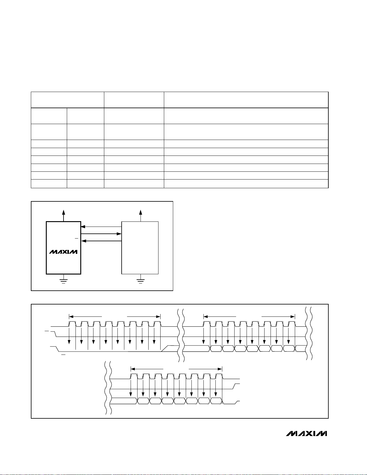
Detailed Description
The MAX1067/MAX1068 low-power, multichannel, 14bit ADCs feature a successive-approximation ADC,
automatic power-down, integrated +4.096V reference,
and a high-speed SPI/QSPI/MICROWIRE-compatible
interface. A DSPR input and DSPX output allow the
MAX1068 to communicate with DSPs with no external
glue logic. The MAX1067/MAX1068 operate with a single +5V analog supply and feature a separate digital
supply allowing direct interfacing with +2.7V to +5.5V
digital logic.
Figures 3 and 4 show the functional diagrams of the
MAX1067/MAX1068, and Figures 5 and 6 show the
MAX1067/MAX1068 in a typical operating circuit. The
serial interface simplifies communication with microprocessors (µPs).
In external reference mode, the MAX1067/MAX1068
have two power modes: normal mode and shutdown
mode. Driving CS high places the MAX1067/MAX1068
in shutdown mode, reducing the supply current to
0.6µA (typ). Pull CS low to place the MAX1067/
MAX1068 in normal operating mode. The internal reference mode offers software-programmable, power-down
options as shown in Table 5.
In SPI/QSPI/MICROWIRE mode, a falling edge on CS
wakes the analog circuitry and allows SCLK to clock in
data. Acquisition and conversion are initiated by SCLK.
The conversion result is available at DOUT in unipolar
serial format. DOUT is held low until data becomes
available (MSB first) on the 8th falling edge of SCLK
when in 8-bit transfer mode, and on the 16th falling
edge when in 16-bit transfer mode. See the Operating
Modes section. Figure 8 shows the detailed SPI/QSPI/
MICROWIRE serial-interface timing diagram.
In external clock mode, the MAX1068 also interfaces
with DSPs. In DSP mode, a frame-sync pulse from the
DSP initiates a conversion that is driven by SCLK. The
MAX1068 formats a frame-sync pulse to notify the DSP
that the conversion results are available at DOUT in
MSB-first, unipolar, serial-data format. Figure 16 shows
the detailed DSP serial-interface timing diagram (see the
Operating Modes section).
Analog Input
Figure 7 illustrates the input-sampling architecture of
the ADC. The voltage applied at REF or the internal
+4.096V reference sets the full-scale input voltage.
Track/Hold (T/H)
In track mode, the analog signal is acquired on the
internal hold capacitor. In hold mode, the T/H switches
open and the capacitive digital-to-analog converter
(DAC) samples the analog input.
MAX1067/MAX1068
Multichannel, 14-Bit, 200ksps Analog-to-Digital
Converters
______________________________________________________________________________________ 11
Pin Description (continued)
Figure 1. Load Circuits for DOUT Enable Time and SCLK-toDOUT Delay Time
Figure 2. Load Circuits for DOUT Disable Time
PIN
MAX1067 MAX1068
NAME FUNCTION
— 13 AIN6 Analog Input 6
— 14 AIN7 Analog Input 7
— 23 DSPX
DSP Frame-Sync Transmit Output. A frame-sync pulse at DSPX notifies the DSP that the
MSB data is available at DOUT. Leave DSPX unconnected when not in DSP mode.
— 24 N.C. No Connection. Not internally connected.
DV
DD
1mA
DOUT
1mA
DGND
a) V
C
LOAD
TO V
OL
OH
= 30pF
DOUT
b) HIGH-Z TO V
C
= 30pF
LOAD
DGND
AND V
TO V
OL
OH
OL
DV
DD
1mA
DOUT
C
1mA
DGND
a) V
TO HIGH-Z
OH
LOAD
= 30pF
DOUT
TO HIGH-Z
b) V
OL
C
LOAD
DGND
= 30pF

MAX1067/MAX1068
During the acquisition, the analog input (AIN_) charges
capacitor C
DAC
. At the end of the acquisition interval
the T/H switches open. The retained charge on C
DAC
represents a sample of the input.
In hold mode, the capacitive DAC adjusts during the
remainder of the conversion cycle to restore node
ZERO to zero within the limits of 14-bit resolution. At the
end of the conversion, force CS high and then low to
reset the T/H switches back to track mode (AIN_),
where C
DAC
charges to the input signal again.
The time required for the T/H to acquire an input signal
is a function of how quickly its input capacitance is
charged. If the input signal’s source impedance is high,
the acquisition time lengthens and more time must be
allowed between conversions. The acquisition time
(t
ACQ
) is the maximum time the device takes to acquire
the signal. Use the following formula to calculate acquisition time:
t
ACQ
= 11(RS+ RIN+ R
DS(ON)
) ✕ 45pF + 0.3µs
where RIN= 340Ω, RS= the input signal’s source
impedance, R
DS(ON)
= 60Ω, and t
ACQ
is never less
than 729ns. A source impedance less than 200Ω does
not significantly affect the ADC’s performance. The
MAX1068 features a 16-bit-wide data-transfer mode
Multichannel, 14-Bit, 200ksps Analog-to-Digital
Converters
12 ______________________________________________________________________________________
Figure 3. MAX1067 Functional Diagram
REFERENCE
REF
AGND
AIN0
AIN1
AIN2
AIN3
SCLK
CS
ANALOG-INPUT
MULTIPLEXER
OSCILLATOR
BIAS
REFCAP
AZ
RAIL
MULTIPLEXER
CONTROL
BUFFER
SUCCESSIVE-APPROXIMATION
AV
DD
MAX1067
DAC
ANALOG-SWITCH FINE TIMING
REGISTER
COMPARATOR
ACCUMULATOR
DV
DD
MEMORY
OUTPUT DOUT
EOC
DIN
INPUT REGISTER
AGND DGND

that includes a longer acquisition time (11.5 clock
cycles). Longer acquisition times are useful in applications with input source resistances greater than 1kΩ.
Noise increases when using large source resistances. To
improve the input signal bandwidth under AC conditions,
drive AIN_ with a wideband buffer (>10MHz) that can
drive the ADC’s input capacitance and settle quickly.
Input Bandwidth
The ADC’s input-tracking circuitry has a 4MHz smallsignal bandwidth, making possible the digitization of
high-speed transient events and the measurement of
periodic signals with bandwidths exceeding the ADC’s
sampling rate by using undersampling techniques. To
avoid aliasing of unwanted, high-frequency signals into
the frequency band of interest, use anti-alias filtering.
Analog Input Protection
Internal protection diodes, which clamp the analog
input to AVDDor AGND, allow the input to swing from
(AGND - 0.3V) to (AVDD+ 0.3V) without damaging the
device. If the analog input exceeds 300mV beyond the
supplies, limit the input current to 10mA.
MAX1067/MAX1068
Multichannel, 14-Bit, 200ksps Analog-to-Digital
Converters
______________________________________________________________________________________ 13
Figure 4. MAX1068 Functional Diagram
AGND
AIN0
AIN1
AIN2
AIN3
AIN4
AIN5
AIN6
AIN7
SCLK
DSEL
DSPR
REF
REFCAP
AZ
RAIL
MULTIPLEXER
CONTROL
BUFFER
REFERENCE
ANALOG-INPUT
MULTIPLEXER
BIAS
OSCILLATOR
CS
AV
DD
DAC
ANALOG-SWITCH FINE TIMING
SUCCESSIVE-APPROXIMATION
REGISTER
DV
MAX1068
COMPARATOR
ACCUMULATOR
MEMORY
DD
OUTPUT DOUT
EOC
DSPX
DIN
INPUT REGISTER
AGND DGND

MAX1067/MAX1068
Digital Interface
The MAX1067/MAX1068 feature an SPI/QSPI/
MICROWIRE-compatible 3-wire serial interface. The
MAX1067 digital interface consists of digital inputs CS,
SCLK, and DIN; and outputs DOUT and EOC. The
MAX1067 operates in the following modes:
• SPI interface with external clock
• SPI interface with internal clock
• SPI interface with internal clock and scan mode
In addition to the standard 3-wire serial interface modes,
the MAX1068 includes a DSPR input and a DSPX output
for communicating with DSPs in external clock mode
and a DSEL input to determine 8-bit-wide or 16-bit-wide
data-transfer mode. When not using the MAX1068 in the
DSP interface mode, connect DSPR to DV
DD
and leave
DSPX unconnected.
Command/Configuration/Control Register
Table 1 shows the contents of the command/configuration/control register and the state of each bit after initial
power-up. Tables 2–6 define the control and configuration of the device for each bit. Cycling the power supplies resets the command/configuration/control register
to the power-on-reset default state.
Initialization After Power-Up
A logic high on CS places the MAX1067/MAX1068 in the
shutdown mode chosen by the power-down bits, and
places DOUT in a high-impedance state. Drive CS low to
power-up and enable the MAX1067/MAX1068 before
starting a conversion. In internal reference mode, allow
5ms for the shutdown internal reference and/or buffer to
wake and stabilize before starting a conversion. In external reference mode (or if the internal reference is already
on), no reference settling time is needed after power-up.
Multichannel, 14-Bit, 200ksps Analog-to-Digital
Converters
14 ______________________________________________________________________________________
Figure 5. MAX1067 Typical Operating Circuit
Figure 6. MAX1068 Typical Operating Circuit
Figure 7. Equivalent Input Circuit
Table 1. Command/Configuration/Control Register
CS
SCLK
DSPX
EOC
CS
SCLK
DSPX
DOUT
EOC
0.1µF
ANALOG
INPUTS
+5V
+5V
DIN
1µF
0.1µF
0.1µF
AIN0
AIN1
AIN2
AIN3
DIN
REF
AV
DV
AIN0
CS
CS
EOC
SCLK
DOUT
EOC
0.1µF
ANALOG
INPUTS
DIN
8
+5V
+5V
16
1µF
0.1µF
0.1µF
SCLK
DOUT
MAX1067
DD
DD
AGND
AGND
DGND
REFCAP
GND
AIN1
AIN2
AIN3
AIN4
AIN5
AIN6
AIN7
DIN
DSEL
DSPR
REF
AV
DV
DOUT
MAX1068
DD
DD
AGND
AGND
DGND
REFCAP
GND
AIN_
MUX
R
DSON
C
MUX
TRACK
HOLD
C
SWITCH
REF
CAPACITIVE
AGND
DAC
C
DAC
HOLD TRACK
ZERO
R
IN
AUTO-ZERO
RAIL
COMMAND
POWER-UP
STATE
BIT7 (MSB) BIT6 BIT5 BIT4 BIT3 BIT2 BIT1 BIT0 (LSB)
CH SEL2 CH SEL1 CH SEL0 SCAN1 SCAN0 REF/PD_SEL1 REF/PD SEL0 INT/EXT CLK
00000110

MAX1067/MAX1068
Multichannel, 14-Bit, 200ksps Analog-to-Digital
Converters
______________________________________________________________________________________ 15
Table 2. Channel Select
Table 3. MAX1067 Scan Mode, Internal
Clock Only
Table 4. MAX1068 Scan Mode, Internal
Clock Only (Not for DSP Mode)
BIT2 BIT1
SEL1
REF/PD
SEL0
REFERENCE
REFERENCE MODE
(INTERNAL REFERENCE)
TYPICAL
SUPPLY
CURRENT
TYPICAL WAKE-
UP TIME
(C
REF
= 1µF)
0 0 Internal
Internal reference and reference buffer stay
on between conversions
1mA NA
0 1 Internal
Internal reference and reference buffer off
between conversions
0.6µA 5ms
1 0 Internal
Internal reference on, reference buffer off
between conversions
0.43mA 5ms
1 1 External Internal reference and buffer always off 0.6µA NA
Table 5. Power-Down Modes
Table 6. Clock Modes
BIT7 BIT6 BIT5
CH SEL2 CH SEL1 CH SEL0
000 0
001 1
010 2
011 3
100 4
101 5
110 6
111 7
CHANNEL
AIN_
ACTION
Single channel, no scan 0 0
Sequentially scan channels 0 through N
(N ≤ 7)
Sequentially scan channels 4 through N
(4 ≤ N ≤ 7)
Scan channel N 8 times 1 1
BIT4 BIT3
SCAN1 SCAN0
01
10
ACTION
Single channel, no scan 0 0
Sequentially scan channels 0 through N
(N ≤ 3)
Sequentially scan channels 2 through N
(2 ≤ N ≤ 3)
Scan channel N 4 times 1 1
BIT4 BIT3
SCAN1 SCAN0
01
10
REF/PD_
BIT0
INT/EXT
CLK
0 External clock
1 Internal clock
CLOCK MODE

MAX1067/MAX1068
Power-Down Modes
Table 5 shows the MAX1067/MAX1068 power-down
modes. Three internal reference modes and one external reference mode are available. Select power-down
modes by writing to bits 2 and 1 in the command/configuration/control register. The MAX1067/MAX1068
enter the selected power-down mode on the rising
edge of CS.
The internal reference stays on when CS is pulled high,
if bits 2 and 1 are set to zero. This mode allows for the
fastest turn-on time.
Setting bit 2 = 0 and bit 1 = 1 turns both the reference
and reference buffer off when CS is brought high. This
mode achieves the lowest supply current. The refer-
ence and buffer wake up on the falling edge of CS
when in SPI/QSPI/MICROWIRE mode and on the falling
edge of DSPR when in DSP mode. Allow 5ms for the
internal reference to rise and settle when powering up
from a complete shutdown (V
REF
= 0, C
REF
= 1µF).
The internal reference stays on and the buffer is shut off
on the rising edge of CS when bit 2 = 1 and bit 1 = 0.
The MAX1067/MAX1068 enter this mode on the rising
edge of CS. The buffer wakes up on the falling edge of
CS when in SPI/QSPI/MICROWIRE mode and on the
falling edge of DSPR when in DSP mode. Allow 5ms for
V
REF
to settle when powering up from a complete shut-
down (V
REF
= 0, C
REF
= 1µF). V
REFCAP
is always equal
to +4.096V in this mode.
Set both bit 2 and bit 1 to 1 to turn off the reference and
reference buffer to allow connection of an external reference. Using an external reference requires no extra
wake-up time.
Operating Modes
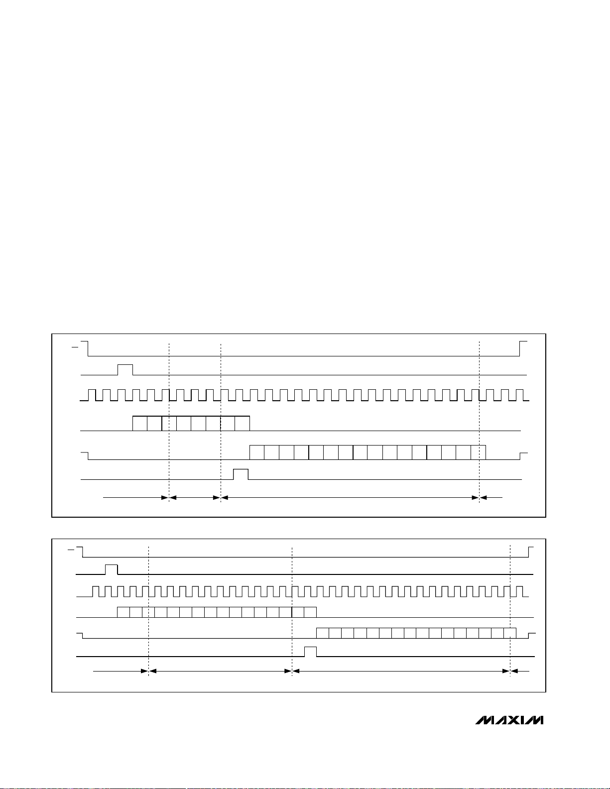
External Clock 8-Bit-Wide Data-Transfer Mode
(MAX1067 and MAX1068)
Force DSPR high and DSEL low (MAX1068) for SPI/
QSPI/MICROWIRE-interface mode. The falling edge of CS
wakes the analog circuitry and allows SCLK to clock in
data. Ensure the duty cycle on SCLK is between 45% and
55% when operating at 4.8MHz (the maximum clock frequency). For lower clock frequencies, ensure the
Multichannel, 14-Bit, 200ksps Analog-to-Digital
Converters
16 ______________________________________________________________________________________
Figure 8. Detailed SPI Interface Timing
Figure 9. Shutdown Sequence
t
CSW
CS
t
SCLK
DIN
DOUT
CSS
t
DS
t
DH
t
DV
t
CL
CS
COMPLETE CONVERSION SEQUENCE
DOUT
CONVERSION 0
POWERED UP
POWERED DOWN
CONVERSION 1
POWERED UP
• • •
t
t
CH
• • •
• • •
• • •
CP
t
DO
t
CSH
t
TR

minimum high and low times are at least 93ns. External
clock-mode conversions with SCLK rates less than
125kHz can reduce accuracy due to leakage of the sampling capacitor. DOUT changes from high-Z to logic low
after CS is brought low. Input data latches on the rising
edge of SCLK. The first SCLK rising edge begins loading
data into the command/configuration/control register from
DIN. The devices select the proper channel for conversion on the rising edge of the 3rd SCLK cycle. Acquisition
begins immediately thereafter and ends on the falling
edge of the 6th clock cycle. The MAX1067/MAX1068
sample the input and begin conversion on the falling
edge of the 6th clock cycle. Setup and configuration of
the MAX1067/MAX1068 complete on the rising edge of
the 8th clock cycle. The conversion result is available
(MSB first) at DOUT on the falling edge of the 8th SCLK
cycle. To read the entire conversion result, 16 SCLK
cycles are needed. Extra clock pulses, occurring after the
conversion result has been clocked out and prior to the
rising edge of CS, cause zeros to be clocked out of
DOUT. The MAX1067/MAX1068 external clock 8-bit-wide
data-transfer mode requires 24 SCLK cycles for completion (Figure 10).
Force CS high after the conversion result is read. For
maximum throughput, force CS low again to initiate the
next conversion immediately after the specified minimum time (t
CSW
). Forcing CS high in the middle of a
conversion immediately aborts the conversion and
places the MAX1067/MAX1068 in shutdown.
External Clock 16-Bit-Wide Data-Transfer Mode
(MAX1068 Only)
Force DSPR high and DSEL high for SPI/QSPI/
MICROWIRE-interface mode. Logic high at DSEL allows
the MAX1068 to transfer data in 16-bit-wide words. The
acquisition time is extended an extra eight SCLK cycles
in the 16-bit-wide data-transfer mode. The falling edge
of CS wakes the analog circuitry and allows SCLK to
clock in data. Ensure the duty cycle on SCLK is
between 45% and 55% when operating at 4.8MHz (the
maximum clock frequency). For lower clock frequencies, ensure that the minimum high and low times are at
least 93ns. External-clock-mode conversions with SCLK
rates less than 125kHz can reduce accuracy due to
leakage of the sampling capacitor. DOUT changes from
high-Z to logic low after CS is brought low. Input data
latches on the rising edge of SCLK. The first SCLK rising
edge begins loading data into the command/configuration/control register from DIN. The devices select the
proper channel for conversion and begin acquisition on
the rising edge of the 3rd SCLK cycle. Setup and configuration of the MAX1068 completes on the rising edge
of the 8th clock cycle. Acquisition ends on the falling
edge of the 14th SCLK cycle. The MAX1068 samples
the input and begins conversion on the falling edge of
the 14th clock cycle. The conversion result is available
(MSB first) at DOUT on the falling edge of the 16th
SCLK cycle. To read the entire conversion result, 16
SCLK cycles are needed. Extra clock pulses, occurring
after the conversion result has been clocked out and
MAX1067/MAX1068
Multichannel, 14-Bit, 200ksps Analog-to-Digital
Converters
______________________________________________________________________________________ 17
Figure 10. SPI External Clock Mode, 8-Bit Data-Transfer Mode, Conversion Timing
CS
1
SCLK
MSB LSB
DIN
DOUT
DSPR*
DSEL*
ADC
STATE
*MAX1068 ONLY
t
ACQ
8
0
MSB LSB
t
CONV
16
24
S1 S0
IDLE

MAX1067/MAX1068
prior to the rising edge of CS, cause zeros to be
clocked out of DOUT. The MAX1068 external clock 16bit-wide data-transfer mode requires 32 SCLK cycles for
completion (Figure 11).
Force CS high after the conversion result is read. For
maximum throughput, force CS low again to initiate the
next conversion immediately after the specified minimum time (t
CSW
). Forcing CS high in the middle of a
conversion immediately aborts the conversion and
places the MAX1068 in shutdown.
Internal Clock 8-Bit-Wide Data-Transfer and
Scan Mode (MAX1067 and MAX1068)
Force DSPR high and DSEL low (MAX1068) for the SPI/
QSPI/MICROWIRE-interface mode. The falling edge of
CS wakes the analog circuitry and allows SCLK to
clock in data (Figure 12). DOUT changes from high-Z
to logic low after CS is brought low. Input data latches
on the rising edge of SCLK. The command/configuration/control register begins reading DIN on the first
SCLK rising edge and ends on the rising edge of the
8th SCLK cycle. The MAX1067/MAX1068 select the
proper channel for conversion on the rising edge of the
3rd SCLK cycle. The internal oscillator activates 125ns
after the rising edge of the 8th SCLK cycle. Turn off the
external clock while the internal clock is on. Turning off
SCLK ensures the lowest noise performance during
acquisition. Acquisition begins on the 2nd rising edge
of the internal clock and ends on the falling edge of the
6th internal clock cycle. Each bit of the conversion
result shifts into memory as it becomes available. The
conversion result is available (MSB first) at DOUT on
the falling edge of EOC. The internal oscillator and analog circuitry are shut down on the high-to-low EOC tran-
Multichannel, 14-Bit, 200ksps Analog-to-Digital
Converters
18 ______________________________________________________________________________________
Figure 11. SPI External Clock Mode, 16-Bit Data-Transfer Mode, Conversion Timing (MAX1068 Only)
Figure 12. SPI Internal Clock Mode, 8-Bit Data-Transfer Mode, Conversion Timing
CS
SCLK
DIN
DOUT
DSPR
DSEL
ADC
STATE
1
MSB
X = DON,T CARE
LSB
8
0
XX
t
ACQ
X
CS
SCLK
INTERNAL
CLK
DOUT
1
MSB
DIN
8
26 25
LSB
1
16 24 32
XXXXX
• • •
MSB
MSB
t
CONV
16924
LSB
S1 S0
LSB
S1 S0 X
IDLE
EOC
ADC
STATE
X = DON,T CARE
DSPR = DV
DD
, DSEL = GND (MAX1068 ONLY)
t
ACQ
t
CONV
IDLE
POWER-DOWN

sition. Use the EOC high-to-low transition as the signal
to restart the external clock (SCLK). To read the entire
conversion result, 16 SCLK cycles are needed. Extra
clock pulses, occurring after the conversion result has
been clocked out and prior to the rising edge of CS,
cause the conversion result to be shifted out again. The
MAX1067/MAX1068 internal clock 8-bit-wide datatransfer mode requires 24 external clock cycles and 25
internal clock cycles for completion.
Force CS high after the conversion result is read. For
maximum throughput, force CS low again to initiate the
next conversion immediately after the specified minimum time (t
CSW
). Forcing CS high in the middle of a
conversion immediately aborts the conversion and
places the MAX1067/MAX1068 in shutdown.
Scan mode allows multiple channels to be scanned
consecutively or one channel to be scanned eight
times. Scan mode can only be enabled when using the
MAX1067/MAX1068 in the internal clock mode. Enable
scanning by setting bits 4 and 3 in the command/configuration/control register (see Tables 3 and 4). In scan
mode, conversion results are stored in memory until the
completion of the last conversion in the sequence.
Upon completion of the last conversion in the
sequence, EOC transitions from high to low to indicate
the end of the conversion and shuts down the internal
oscillator. Use the EOC high-to-low transition as the signal to restart the external clock (SCLK). DOUT provides
the conversion results in the same order as the channel
conversion process. The MSB of the first conversion is
available at DOUT on the falling edge of EOC (Figure 14).
MAX1067/MAX1068
Multichannel, 14-Bit, 200ksps Analog-to-Digital
Converters
______________________________________________________________________________________ 19
Figure 13. SPI Internal Clock Mode,16-Bit Data-Transfer Mode, Conversion Timing (MAX1068 Only)
Figure 14. SPI Internal Clock Mode, 8-Bit Data-Transfer Mode, Scan Mode for Two Conversions, Conversion Timing
SCLK
INTERNAL
CLK
DIN
DOUT
EOC
ADC
STATE
CS
1
• • • • • •
DATA
CONFIGURATION
X = DON,T CARE
DSPR = DSEL = DV
89 16
X X X X X X X X
DD
21332
t
ACQ
• • •• • •
MSB
t
CONV
POWER-DOWN
SCLK
INTERNAL
CLK
DIN
DOUT
CS
MSB
1
LSB
8
2
1
6
24
• • • • • •
3026
48
2417 32
LSB
S1 S0 X
940
MSB
• • •
• • •
LSB
S1 S0 X
EOC
ADC
STATE
CONFIGURATION
X = DON,T CARE
DSPR = DV
DD
, DSEL = GND (MAX1068 ONLY)
t
ACQ
t
CONV
t
ACQ
t
CONV
POWER-DOWN

MAX1067/MAX1068
Internal Clock 16-Bit-Wide Data-Transfer and
Scan Mode (MAX1068 Only)
Force DSPR high and DSEL low for the SPI/QSPI/
MICROWIRE-interface mode. The falling edge of CS
wakes the analog circuitry and allows SCLK to clock in
data (see Figure 13). DOUT changes from high-Z to logic
low after CS is brought low. Input data latches on the rising edge of SCLK. The command/configuration/control
register begins reading DIN on the first SCLK rising
edge and ends on the rising edge of the 8th SCLK
cycle. The MAX1068 selects the proper channel for
conversion on the rising edge of the 3rd SCLK cycle.
The internal oscillator activates 125ns after the rising
edge of the 16th SCLK cycle. Turn off the external
clock while the internal clock is on. Turning off SCLK
ensures lowest noise performance during acquisition.
Acquisition begins on the 2nd rising edge of the internal clock and ends on the falling edge of the 18th internal clock cycle. Each bit of the conversion result shifts
into memory as it becomes available. The conversion
result is available (MSB first) at DOUT on the falling
edge of EOC. The internal oscillator and analog circuitry are shut down on the EOC high-to-low transition. Use
the EOC high-to-low transition as the signal to restart
the external clock (SCLK). To read the entire conversion result, 16 SCLK cycles are needed. Extra clock
pulses, occurring after the conversion result has been
clocked out and prior to the rising edge of CS, cause
the conversion result to be shifted out again. The
MAX1068 internal-clock 16-bit-wide data-transfer mode
requires 32 external clock cycles and 32 internal clock
cycles for completion.
Force CS high after the conversion result is read. For
maximum throughput, force CS low again to initiate the
next conversion immediately after the specified minimum time (t
CSW
). Forcing CS high in the middle of a
conversion immediately aborts the conversion and
places the MAX1068 in shutdown.
Scan mode allows multiple channels to be scanned
consecutively or one channel to be scanned eight
times. Scan mode can only be enabled when using the
MAX1068 in internal clock mode. Enable scanning by
setting bits 4 and 3 in the command/configuration/control register (see Tables 3 and 4). In scan mode, conversion results are stored in memory until the completion of
the last conversion in the sequence. Upon completion of
the last conversion in the sequence, EOC transitions
from high to low to indicate the end of the conversion
and shuts down the internal oscillator. Use the EOC
high-to-low transition as the signal to restart the external
clock (SCLK). DOUT provides the conversion results in
the same order as the channel conversion process. The
MSB of the first conversion is available at DOUT on the
falling edge of EOC. Figure 15 shows the timing diagram for 16-bit-wide data transfer in scan mode.
Multichannel, 14-Bit, 200ksps Analog-to-Digital
Converters
20 ______________________________________________________________________________________
Figure 15. SPI Internal Clock Mode, 16-Bit Data-Transfer Mode, Scan Mode for Two Conversions, Conversion Timing (MAX1068 Only)
CS
SCLK
INTERNAL
CLK
DOUT
EOC
ADC
STATE
1
DIN
89 16
• • • • • •
DATA
X = DON,T CARE
X X X X X X X X
2
t
13
ACQ
32 34
CONV
45
• • • • • •• • • • • •
t
ACQ
t
CONV
17
• • •
64
MSB
• • •
POWER-DOWNt
48
LSB
S1 S0 X

DSP 8-Bit-Wide Data-Transfer Mode (External Clock
Mode, MAX1068 Only)
Figure 16 shows the DSP-interface timing diagram.
Logic low at DSPR on the falling edge of CS enables
DSP interface mode. After the MAX1068 enters DSP
mode, CS can remain low for the duration of the conversion process and each subsequent conversion.
Drive DSEL low to select the 8-bit data-transfer mode.
A sync pulse from the DSP at DSPR wakes the analog
circuitry and allows SCLK to clock in data (Figure 17).
The frame sync pulse alerts the MAX1068 that incoming data is about to be sent to DIN. Ensure the duty
cycle on SCLK is between 45% and 55% when operating at 4.8MHz (the maximum clock frequency). For
lower clock frequencies, ensure the minimum high and
low times are at least 93ns. External clock mode conversions with SCLK rates less than 125kHz can reduce
accuracy due to leakage of the sampling capacitor.
The input data latches on the falling edge of SCLK. The
command/configuration/control register starts reading
data in on the falling edge of the first SCLK cycle immediately following the falling edge of the frame sync
pulse and ends on the falling edge of the 8th SCLK
cycle. The MAX1068 selects the proper channel for
conversion on the falling edge of the 3rd clock cycle
and begins acquisition. Acquisition continues until the
rising edge of the 7th clock cycle. The MAX1068 samples the input on the rising edge of the 7th clock cycle.
On the rising edge of the 8th clock cycle, the MAX1068
outputs a frame sync pulse at DSPX. The frame sync
pulse alerts the DSP that the conversion results are
about to be output at DOUT (MSB first) starting on the
rising edge of the 9th clock pulse. To read the entire
conversion results, 16 SCLK cycles are needed. Extra
clock pulses, occuring after the conversion result has
been clocked out, and prior to the next rising edge of
DSPR, cause zeros to be clocked out of DOUT. The
MAX1068 external-clock, DSP 8-bit-wide data-transfer
mode requires 24 clock cycles to complete.
Begin a new conversion by sending a new frame sync
pulse to DSPR followed by new configuration data.
Send the new DSPR pulse immediately after reading
the conversion result to realize maximum throughput.
Sending a new frame sync pulse in the middle of a conversion immediately aborts the current conversion and
begins a new one. A rising edge on CS in the middle of
a conversion aborts the current conversion and places
the MAX1068 in shutdown.
DSP 16-Bit-Wide Data-Transfer Mode (External
Clock Mode, MAX1068 Only)
Figure 16 shows the DSP-interface timing diagram. Logic
low at DSPR on the falling edge of CS enables DSP interface mode. After the MAX1068 enters DSP mode, CS
can remain low for the duration of the conversion
process and each subsequent conversion. The acquisition time is extended an extra eight SCLK cycles in the
16-bit-wide data-transfer mode. Drive DSEL high to
select the 16-bit-wide data-transfer mode. A sync pulse
from the DSP at DSPR wakes the analog circuitry and
allows SCLK to clock in data (Figure 18). The frame
sync pulse also alerts the MAX1068 that incoming data
is about to be sent to DIN. Ensure the duty cycle on
SCLK is between 45% and 55% when operating at
MAX1067/MAX1068
Multichannel, 14-Bit, 200ksps Analog-to-Digital
Converters
______________________________________________________________________________________ 21
Figure 16. Detailed DSP-Interface Timing (MAX1068 Only)
t
CSW
CS
t
DF
t
DSPR
SCLK
DOUT
t
CSS
t
CP
DIN
t
DV
FSS
t
FSH
t
t
CL
CH
...
...
t
CSH
...
t
DS
t
DH
...
t
DO
t
TR
...
MAX1067/MAX1068
4.8MHz (the maximum clock frequency). For lower
clock frequencies, ensure the minimum high and low
times are at least 93ns. External-clock-mode conversions with SCLK rates less than 125kHz can reduce
accuracy due to leakage of the sampling capacitor.
The input data latches on the falling edge of SCLK. The
command/configuration/control register starts reading
data in on the falling edge of the first SCLK cycle immediately following the falling edge of the frame sync
pulse and ends on the falling edge of the 16th SCLK
cycle. The MAX1068 selects the proper channel for
conversion on the falling edge of the 3rd clock cycle
and begins acquisition. Acquisition continues until the
rising edge of the 15th clock cycle. The MAX1068 samples the input on the rising edge of the 15th clock cycle.
On the rising edge of the 16th clock cycle, the MAX1068
outputs a frame sync pulse at DSPX. The frame sync
pulse alerts the DSP that the conversion results are
about to be output at DOUT (MSB first) starting on the
rising edge of the 17th clock pulse. To read the entire
conversion result, 16 SCLK cycles are needed. Extra
clock pulses, occuring after the conversion result has
been clocked out and prior to the next rising edge of
DSPR, cause zeros to be clocked out of DOUT. The
MAX1068 external clock, DSP 16-bit-wide data-transfer
mode requires 32 clock cycles to complete.
Begin a new conversion by sending a new frame sync
pulse to DSPR followed by new configuration data.
Send the new DSPR pulse immediately after reading
the conversion result to realize maximum throughput.
Sending a new frame sync pulse in the middle of a conversion immediately aborts the current conversion and
begins a new one. A rising edge on CS in the middle of
a conversion aborts the current conversion and places
the MAX1068 in shutdown.
Multichannel, 14-Bit, 200ksps Analog-to-Digital
Converters
22 ______________________________________________________________________________________
Figure 17. DSP External Clock Mode, 8-Bit Data-Transfer Mode, Conversion Timing (MAX1068 Only)
Figure 18. DSP External Clock Mode, 16-Bit Data-Transfer Mode, Conversion Timing (MAX1068 Only)
DSPR
SCLK
DIN
DOUT
CS
1
MSB
8
LSB
0
16
MSB LSB
24
S1 S0
DSPX
ADC
STATE
t
ACQ
t
CONV
CS
DSPR
SCLK
DIN
DOUT
DSPX
ADC
STATE
X = DON,T CARE
1
MSB
8
LSB
0
XX
t
ACQ
X
16 24 32
XXXXX
MSB
t
CONV
LSB
IDLE
S0
S1
IDLE

MAX1067/MAX1068
Multichannel, 14-Bit, 200ksps Analog-to-Digital
Converters
______________________________________________________________________________________ 23
Output Coding and Transfer Function
The data output from the MAX1067/MAX1068 is
straight binary. Figure 19 shows the nominal transfer
function. Code transitions occur halfway between successive integer LSB values (V
REF
= +4.096V, and
1 LSB = +250µV or 4.096V / 16,384V).
Applications Information
Internal Reference
The internal bandgap reference provides a buffered
+4.096V. Bypass REFCAP with a 0.1µF capacitor to
AGND and REF with a 1µF capacitor to AGND. For best
results, use low-ESR, X5R/X7R ceramic capacitors.
Allow 5ms for the reference and buffer to wake up from
full power-down (see Table 5).
External Reference
The MAX1067/MAX1068 accept an external reference
with a voltage range between +3.8V and AVDD.
Connect the external reference directly to REF. Bypass
REF to AGND with a 10µF capacitor. When not using a
low-ESR bypass capacitor, use a 0.1µF ceramic capacitor in parallel with the 10µF capacitor. Noise on the reference degrades conversion accuracy.
The input impedance at REF is 37kΩ for DC currents.
During a conversion, the external reference at REF
must deliver 118µA of DC load current and have an
output impedance of 10Ω or less.
For optimal performance, buffer the reference through
an op amp and bypass the REF input. Consider the
equivalent input noise (82µV
RMS
) of the MAX1067/
MAX1068 when choosing a reference.
Internal/External Oscillator
Select either an external (0.1MHz to 4.8MHz) or the
internal 4MHz (typ) clock to perform conversions
(Table 6). The external clock shifts data in and out of
the MAX1067/MAX1068 in either clock mode.
When using the internal clock mode, the internal oscillator controls the acquisition and conversion processes, while the external oscillator shifts data in and out of
the MAX1067/MAX1068. Turn off the external clock
(SCLK) when the internal clock is on to realize lowest
noise performance. The internal clock remains off in
external clock mode.
Input Buffer
Most applications require an input-buffer amplifier to
achieve 14-bit accuracy. The input amplifier must have
a slew rate of at least 2V/µs and a unity-gain bandwidth
of at least 10MHz to complete the required output-voltage change before the end of the acquisition time.
At the beginning of the acquisition, the internal sampling capacitor array connects to AIN_ (the amplifier
input), causing some disturbance on the output of the
buffer. Ensure the sampled voltage has settled before
the end of the acquisition time.
Digital Noise
Digital noise can couple to AIN_ and REF. The conversion clock (SCLK) and other digital signals active during
input acquisition contribute noise to the conversion
result. Noise signals, synchronous with the sampling
interval, result in an effective input offset. Asynchronous
signals produce random noise on the input, whose highfrequency components can be aliased into the frequency band of interest. Minimize noise by presenting a low
impedance (at the frequencies contained in the noise
signal) at the inputs. This requires bypassing AIN_ to
AGND, or buffering the input with an amplifier that has a
small-signal bandwidth of several megahertz (doing both
is preferable). AIN has a typical bandwidth of 4MHz.
Figure 19. Unipolar Transfer Function, Full Scale (FS) = V
REF
,
Zero Scale (ZS) = GND
OUTPUT CODE
FULL-SCALE
11...111
11...110
11...101
00...011
00...010
00...001
00...000
0
123
INPUT VOLTAGE (LSB)
TRANSITION
FS = V
1 LSB =
FS - 3/2 LSB
REF
V
REF
16,384
FS
MAX1067/MAX1068
Multichannel, 14-Bit, 200ksps Analog-to-Digital
Converters
24 ______________________________________________________________________________________
Distortion
Avoid degrading dynamic performance by choosing an
amplifier with distortion much less than the total harmonic
distortion of the MAX1067/MAX1068 at the frequencies of
interest (THD = -98db at 1kHz). If the chosen amplifier
has insufficient common-mode rejection, which results in
degraded THD performance, use the inverting configuration (positive input grounded) to eliminate errors from this
source. Low-temperature-coefficient, gain-setting resistors reduce linearity errors caused by resistance
changes due to self-heating. To reduce linearity errors
due to finite amplifier gain, use amplifier circuits with sufficient loop gain at the frequencies of interest..
DC Accuracy
To improve DC accuracy, choose a buffer with an offset
much less than the MAX1067/MAX1068s’ offset (±10mV
max for +5V supply), or whose offset can be trimmed
while maintaining stability over the required temperature range.
Serial Interfaces
SPI and MICROWIRE Interfaces
When using the SPI (Figure 20a) or MICROWIRE (Figure
20b) interfaces, set CPOL = 0 and CPHA = 0. Drive CS
low to power on the MAX1067/MAX1068 before starting a
conversion (Figure 20c). Three consecutive 8-bit-wide
readings are necessary to obtain the entire 14-bit result
from the ADC. DOUT data transitions on the serial clock’s
falling edge. The first 8-bit-wide data stream contains all
leading zeros. The 2nd 8-bit-wide data stream contains
the MSB through D6. The 3rd 8-bit-wide data stream contains D5 through D0 followed by S1 and S0.
Figure 20a. SPI Connections
Figure 20b. MICROWIRE Connections
Figure 20c. SPI/MICROWIRE Interface Timing Sequence (CPOL = CPHA = 0)
I/O
SCK
MISO
SPI
SS
V
DD
CS
SCLK
DOUT
MAX1067
MAX1068
CS
SCLK
DOUT
MAX1067
MAX1068
MICROWIRE
I/O
SK
SI
1ST BYTE READ
SCLK
CS
DOUT*
*WHEN CS IS HIGH, DOUT = HIGH-Z
641
8
00000000
3RD BYTE READ
2ND BYTE READ
D13 D12 D11 D10 D9 D8 D7 D6 D5
MSB
2420
S1 S0D5 D4 D3 D2 D1 D0
LSB
HIGH-Z
1612

MAX1067/MAX1068
Multichannel, 14-Bit, 200ksps Analog-to-Digital
Converters
______________________________________________________________________________________ 25
QSPI Interface
Using the high-speed QSPI interface with CPOL = 0
and CPHA = 0, the MAX1067/MAX1068 support a
maximum f
SCLK
of 4.8MHz. Figure 21a shows the
MAX1067/MAX1068 connected to a QSPI master and
Figure 21b shows the associated interface timing.
PIC16 with SSP Module and PIC17
Interface
The MAX1067/MAX1068 are compatible with a PIC16/
PIC17 controller (µC), using the synchronous serial-port
(SSP) module.
To establish SPI communication, connect the controller
as shown in Figure 22a and configure the PIC16/PIC17
as system master by initializing its synchronous serialport control register (SSPCON) and synchronous serialport status register (SSPSTAT) to the bit patterns shown
in Tables 7 and 8.
In SPI mode, the PIC16/PIC17 µCs allow 8 bits of data to
be synchronously transmitted and received simultaneously. Three consecutive 8-bit-wide readings (Figure
22b) are necessary to obtain the entire 14-bit result from
the ADC. DOUT data transitions on the serial clock’s
falling edge and is clocked into the µC on SCLK’s rising
edge. The first 8-bit-wide data stream contains all zeros.
The 2nd 8-bit-wide data stream contains the MSB
through D6. The 3rd 8-bit-wide data stream contains bits
D5 through D0 followed by S1 and S0.
Figure 21b. QSPI Interface Timing Sequence (External Clock, 8-Bit Data Transfer, CPOL = CPHA = 0)
Table 7. Detailed SSPCON Register Contents
X = Don’t care.
Figure 21a. QSPI Connections
V
DD
CS
SCLK
DOUT
MAX1067
MAX1068
SAMPLING INSTANT
D13 D12 D11
MSB
CS
SCK
MISO
QSPI
SS
SCLK
CS
DOUT*
*WHEN CS IS HIGH, DOUT = HIGH-Z
1214 86
D10 D9 D8 D7
D6 D3
D5 D4
2016
D2 D1
D0
LSB
24
S1
HIGH-Z
S0
CONTROL BIT SETTINGS SYNCHRONOUS SERIAL-PORT CONTROL REGISTER (SSPCON)
WCOL BIT7 X Write Collision Detection Bit
SSPOV BIT6 X Receive Overflow Detection Bit
Synchronous Serial-Port Enable Bit:
SSPEN BIT5 1
CKP BIT4 0 Clock Polarity Select Bit. CKP = 0 for SPI master-mode selection.
SSPM3 BIT3 0
SSPM2 BIT2 0
SSPM1 BIT1 0
SSPM0 BIT0 1
0: Disables serial port and configures these pins as I/O port pins.
1: Enables serial port and configures SCK, SDO, and SCI pins as serial
port pins.
Synchronous Serial-Port Mode Select Bit. Sets SPI master-mode and
= f
selects f
CLK
OSC
/ 16.
DSP Interface
The DSP mode of the MAX1068 only operates in external clock mode. Figure 23 shows a typical DSP interface
connection to the MAX1068. Use the same oscillator as
the DSP to provide the clock signal for the MAX1068.
The DSP provides the falling edge at CS to wake the
MAX1068. The MAX1068 detects the state of DSPR on
the falling edge of CS (Figure 17). Logic low at DSPR
places the MAX1068 in DSP mode. After the MAX1068
enters DSP mode, CS can be left low. A frame sync
pulse from the DSP to DSPR initiates a conversion. The
MAX1068 sends a frame sync pulse from DSPX to the
DSP signaling that the MSB is available at DOUT. Send
another frame sync pulse from the DSP to DSPR to
begin the next conversion. The MAX1068 does not
operate in scan mode when using DSP mode.
MAX1067/MAX1068
Multichannel, 14-Bit, 200ksps Analog-to-Digital
Converters
26 ______________________________________________________________________________________
Figure 22b. SPI Interface Timing with PIC16/PIC17 in Master Mode (CKE = 1, CKP = 0, SMP = 0, SSPM3 - SSPM0 = 0001)
Figure 22a. SPI Interface Connection for a PIC16/PIC17
Table 8. Detailed SSPSTAT Register Contents
X = Don’t care.
CONTROL BIT SETTINGS SYNCHRONOUS SERIAL-PORT STATUS REGISTER (SSPSTAT)
SMP BIT7 0
CKE BIT6 1
D/A BIT5 X Data Address Bit
P BIT4 X Stop Bit
S BIT3 X Start Bit
R/W BIT2 X Read/Write Bit Information
UA BIT1 X Update Address
BF BIT0 X Buffer-Full Status Bit
V
DD
MAX1067
MAX1068
SCLK
DOUT
CS
GND
V
SCK
SDI
I/O
PIC16/17
SPI Data-Input Sample Phase. Input data is sampled at the middle of
the data output time.
SPI Clock Edge-Select Bit. Data is transmitted on the rising edge of the
serial clock.
DD
1ST BYTE READ
SCLK
CS
DOUT*
*WHEN CS IS HIGH, DOUT = HIGH-Z
00000000
3RD BYTE READ
20
LSB
D12 D11 D10 D9 D8 D7 D6
D13
MSB
24
S1 S0D5 D4 D3 D2 D1 D0
2ND BYTE READ
16128641
HIGH-Z

MAX1067/MAX1068
Multichannel, 14-Bit, 200ksps Analog-to-Digital
Converters
______________________________________________________________________________________ 27
Definitions
Integral Nonlinearity
Integral nonlinearity (INL) is the deviation of the values
on an actual transfer function from a straight line. This
straight line can be either a best-straight-line fit or a line
drawn between the end points of the transfer function,
once offset and gain errors have been nullified. The
static linearity parameters for the MAX1067/MAX1068
are measured using the end-point method.
Differential Nonlinearity
Differential nonlinearity (DNL) is the difference between
an actual step-width and the ideal value of ±1 LSB. A
DNL error specification of ±1 LSB guarantees no missing codes and a monotonic transfer function.
Aperture Definitions
Aperture jitter (tAJ) is the sample-to-sample variation in
the time between samples. Aperture delay (tAD) is the
time between the falling edge of the sampling clock
and the instant when the actual sample is taken.
Signal-to-Noise Ratio
For a waveform perfectly reconstructed from digital
samples, signal-to-noise ratio (SNR) is the ratio of the
full-scale analog input (RMS value) to the RMS quantization error (residual error). The ideal, theoretical minimum analog-to-digital noise is caused by quantization
noise error only and results directly from the ADC’s resolution (N bits):
SNR = (6.02 ✕ N + 1.76)dB
In reality, there are other noise sources besides quantization noise: thermal noise, reference noise, clock jitter,
etc. SNR is computed by taking the ratio of the RMS
signal to the RMS noise, which includes all spectral
components minus the fundamental, the first five harmonics, and the DC offset.
Signal-to-Noise Plus Distortion
Signal-to-noise plus distortion (SINAD) is the ratio of the
fundamental input frequency’s RMS amplitude to the
RMS equivalent of all the other ADC output signals:
SINAD (dB) = 20 ✕ log [Signal
RMS
/ (Noise +
Distortion)
RMS
]
Effective Number of Bits
Effective number of bits (ENOB) indicates the global
accuracy of an ADC at a specific input frequency and
sampling rate. An ideal ADC’s error consists of quantization noise only. With an input range equal to the fullscale range of the ADC, calculate the ENOB as follows:
ENOB = (SINAD - 1.76) / 6.02
Figure 24 shows the ENOB as a function of the MAX1067/
MAX1068s’ input frequency.
Figure 23. DSP Interface Connection
Figure 24. Effective Bits vs. Frequency
EXTERNAL
CLOCK
SCLK
TFS
RFS
DSP
DT
DR
FL1
SCLK
DSPR
DSPX
DIN
DOUT
CS
MAX1068
EFFECTIVE NUMBER OF BITS (ENOB)
16
14
12
10
8
6
EFFECTIVE BITS
4
2
f
= 200ksps
SAMPLE
0
0.1 10 100
1
FREQUENCY (kHz)

Total Harmonic Distortion
Total harmonic distortion (THD) is the ratio of the RMS
sum of the first five harmonics of the input signal to the
fundamental itself. This is expressed as:
where V1is the fundamental amplitude and V2through
V5are the 2nd- through 5th-order harmonics.
Spurious-Free Dynamic Range
Spurious-free dynamic range (SFDR) is the ratio of the
RMS amplitude of the fundamental (maximum signal
component) to the RMS value of the next-largest frequency component.
Supplies, Layout, Grounding, and
Bypassing
Use printed circuit (PC) boards with separate analog
and digital ground planes. Do not use wire-wrap
boards. Connect the two ground planes together at the
MAX1067/MAX1068 AGND terminal. Isolate the digital
supply from the analog with a low-value resistor (10Ω)
or ferrite bead when the analog and digital supplies
come from the same source (Figure 25).
Constraints on sequencing the power supplies and
inputs are as follows:
• Apply AGND before DGND.
• Apply AIN_ and REF after AVDDand AGND are
present.
• DVDDis independent of the supply sequencing.
Ensure that digital return currents do not pass through
the analog ground and that return-current paths are low
impedance. A 5mA current flowing through a PC board
ground trace impedance of only 0.05Ω creates an error
voltage of about 250µV and a 1 LSB error with a +4.096V
full-scale system.
The board layout should ensure that digital and analog
signal lines are kept separate. Do not run analog and digital lines (especially the SCLK and DOUT) parallel to one
another. If one must cross another, do so at right angles.
The ADC’s high-speed comparator is sensitive to highfrequency noise on the AVDDpower supply. Bypass an
excessively noisy supply to the analog ground plane
with a 0.1µF capacitor in parallel with a 1µF to 10µF
low-ESR capacitor. Keep capacitor leads short for best
supply-noise rejection.
MAX1067/MAX1068
Multichannel, 14-Bit, 200ksps Analog-to-Digital
Converters
28 ______________________________________________________________________________________
Figure 25. Powering AVDDand DVDDfrom a Single Supply
T
HD
=×
202log
+V +V +V
V
232425
2
V
1
AIN_
+5V
1µF
0.1µF
10Ω
AIN_
REF
AV
DD
MAX1067
MAX1068
SCLK
DOUT
CS
CS
SCLK
DOUT
DV
DD
0.1µF
AGND
AGND
DGND
GND
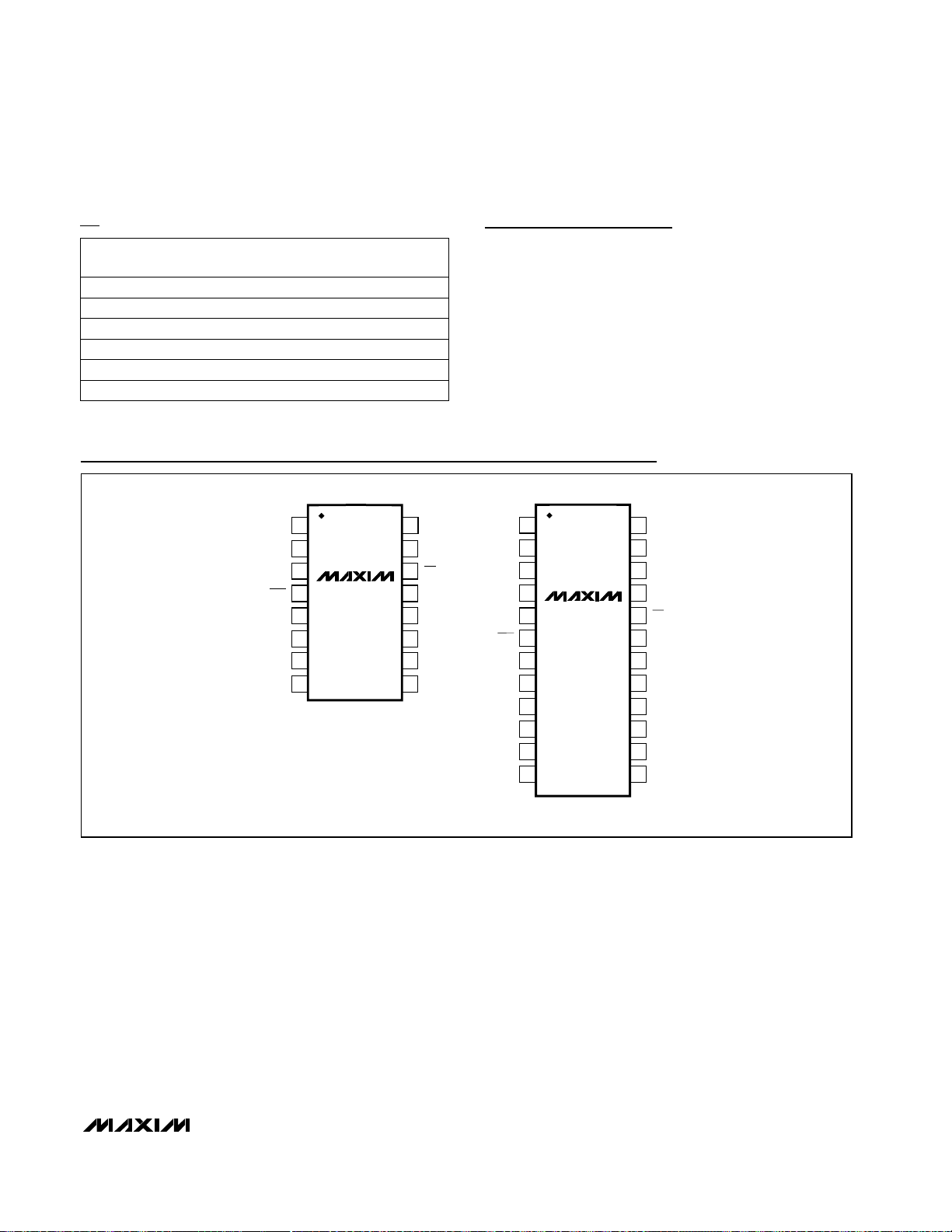
MAX1067/MAX1068
Multichannel, 14-Bit, 200ksps Analog-to-Digital
Converters
______________________________________________________________________________________ 29
Pin Configurations
Chip Information
TRANSISTOR COUNT: 20,760
PROCESS: BiCMOS
Ordering Information (continued)
*Future product—contact factory for availability.
PART TEMP RANGE
PINPACKAGE
INL
(LSB)
MAX1068ACEG 0°C to +70°C 24 QSOP ± 0.5
MAX1068BCEG 0°C to +70°C 24 QSOP ±1
MAX1068CCEG 0°C to +70°C 24 QSOP ±2
MAX1068AEEG* -40°C to +85°C 24 QSOP ±0.5
MAX1068BEEG* -40°C to +85°C 24 QSOP ±1
MAX1068CEEG* -40°C to +85°C 24 QSOP ±2
TOP VIEW
DOUT
SCLK
DIN
EOC
AIN0
AIN1
AIN2
AIN3
1
2
3
MAX1067
4
5
6
7
8
16
15
14
13
12
11
10
9
QSOP
DV
DD
DGND
CS
AV
DD
AGND
AGND
REFCAP
REF
DSPR
DSEL
DOUT
DIN
EOC
AIN0
AIN2
AIN3
AIN4
1
2
3
4
MAX1068
5
6
7
8
9
10
11
12
24
23
22
21
20
19
18
17
16
15
14
13
N.C.
DSPX
DV
DD
DGNDSCLK
CS
AV
DD
AGND
AGNDAIN1
REFCAP
REF
AIN7
AIN6AIN5
QSOP

MAX1067/MAX1068
Multichannel, 14-Bit, 200ksps Analog-to-Digital
Converters
Maxim cannot assume responsibility for use of any circuitry other than circuitry entirely embodied in a Maxim product. No circuit patent licenses are
implied. Maxim reserves the right to change the circuitry and specifications without notice at any time.
30 ____________________Maxim Integrated Products, 120 San Gabriel Drive, Sunnyvale, CA 94086 408-737-7600
© 2003 Maxim Integrated Products Printed USA is a registered trademark of Maxim Integrated Products.
Package Information
(The package drawing(s) in this data sheet may not reflect the most current specifications. For the latest package outline information,
go to www.maxim-ic.com/packages
.)
QSOP.EPS
PACKAGE OUTLINE, QSOP .150", .025" LEAD PITCH
21-0055
1
E
1
 Loading...