

General Description
The MAX1065/MAX1066 14-bit, low-power successive
approximation analog-to-digital converters (ADCs) feature automatic power-down, a factory-trimmed internal
clock, and a high-speed, 14-bit-wide (MAX1065) or
byte-wide (MAX1066) parallel interface. The devices
operate from a single 4.75V to 5.25V analog supply and
a 2.7V to 5.25V digital supply.
The MAX1065/MAX1066 use an internal 4.096V reference or an external reference. The MAX1065/MAX1066
consume only 1.8mA at a sampling rate of 165ksps with
external reference and 2.7mA with internal reference.
AutoShutdown™ reduces supply current to 0.1mA at
10ksps.
The MAX1065/MAX1066 are ideal for high-performance,
battery-powered, data-acquisition applications.
Excellent dynamic performance and low-power consumption in a small package make the MAX1065/
MAX1066 the best choice for circuits with demanding
power consumption and space requirements.
The 14-bit-wide MAX1065 is available in a 28-pin TSSOP
package, and the byte-wide MAX1066 is available in a
20-pin TSSOP package. Both devices are available in
either the 0°C to +70°C commercial, or the -40°C to
+85°C extended temperature range.
Applications
Features
♦ 14-Bit-Wide (MAX1065) and Byte-Wide (MAX1066)
Parallel Interface
♦ High Speed: 165ksps Sample Rate
♦ Accurate: ±1LSB DNL (max), ±1LSB INL (max)
♦ 4.096V, 35ppm/°C Internal Reference
♦ External Reference Range 3.8V to 5.25V
♦ Single 4.75V to 5.25V Analog Supply Voltage
♦ 2.7V to 5.25V Digital Supply Voltage
♦ Low Supply Current
1.8mA (External Reference)
2.7mA (Internal Reference)
0.1mA AutoShutdown Mode (10ksps, External
Reference)
♦ Small Footprint
28-Pin TSSOP Package (14-Bit Wide)
20-Pin TSSOP Package (Byte Wide)
MAX1065/MAX1066
Low-Power, 14-Bit Analog-to-Digital Converters
with Parallel Interface
________________________________________________________________ Maxim Integrated Products 1
Ordering Information
ANALOG INPUT
D0–D13
EOC
REFADJ
REF
DGNDAGND
RESET
CS
R/C
AIN
AV
DD
DV
DD
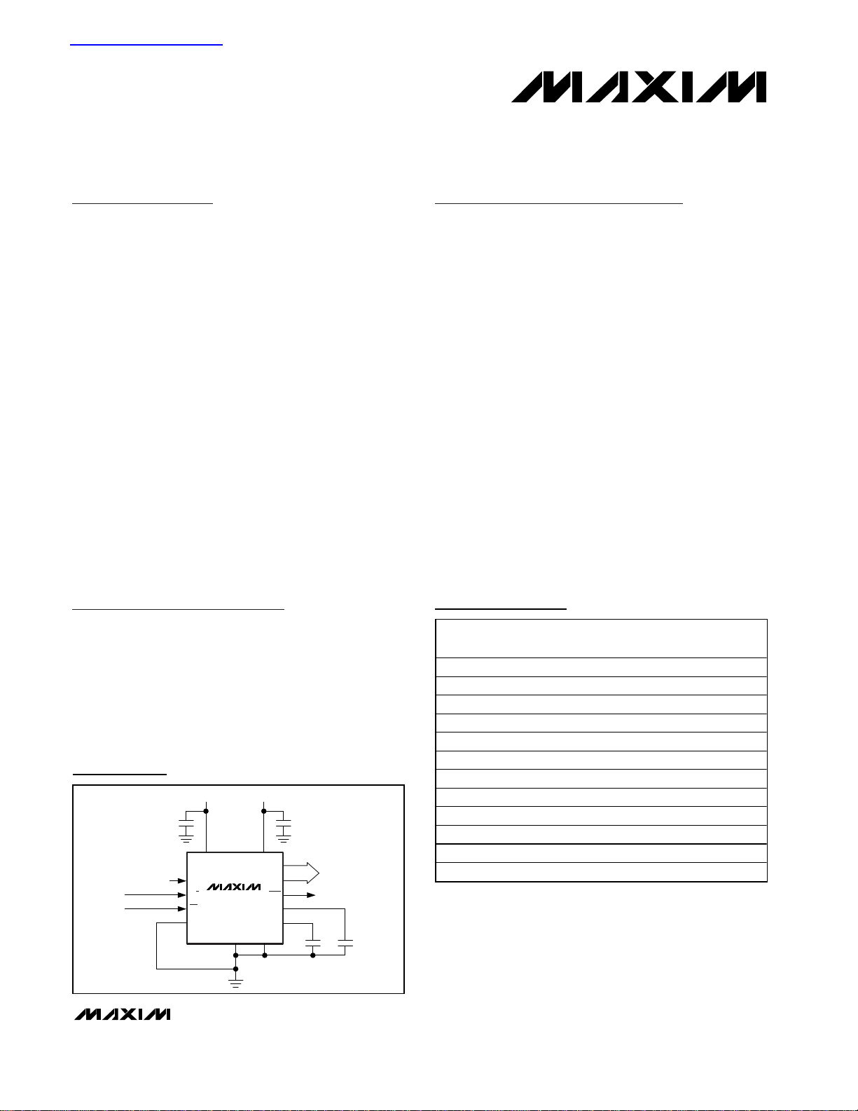
MAX1065
0.1µF 0.1µF
5V ANALOG 5V DIGITAL
0.1µF1µF
µP DATA
BUS
Typical Operating Circuit
19-2466; Rev 0; 4/02
For pricing, delivery, and ordering information, please contact Maxim/Dallas Direct! at
1-888-629-4642, or visit Maxim’s website at www.maxim-ic.com.
Pin Configurations appear at end of data sheet.
AutoShutdown is a registered trademark of Maxim Integrated
Products, Inc.
PART
PIN-
INL
MAX1065ACUI 0°C to 70°C
±1
MAX1065BCUI 0°C to 70°C
±2
MAX1065CCUI 0°C to 70°C
±3
MAX1065AEUI
±1
MAX1065BEUI
±2
MAX1065CEUI
±3
MAX1066ACUP
0°C to 70°C
±1
MAX1066BCUP
0°C to 70°C
±2
MAX1066CCUP
0°C to 70°C
±3
MAX1066AEUP
±1
MAX1066BEUP
±2
MAX1066CEUP
±3
Temperature
Sensor/Monitor
Industrial Process
Control
I/O Boards
Data-Acquisition
Systems
Cable/Harness Tester
Accelerometer
Measurements
Digital Signal Processing
查询MAX1065供应商
TEMP RANGE
PACKAGE
28 TSSOP
28 TSSOP
28 TSSOP
-40°C to +85°C 28 TSSOP
-40°C to +85°C 28 TSSOP
-40°C to +85°C 28 TSSOP
20 TSSOP
20 TSSOP
20 TSSOP
-40°C to +85°C 20 TSSOP
-40°C to +85°C 20 TSSOP
-40°C to +85°C 20 TSSOP
MAX1065/MAX1066
Low-Power, 14-Bit Analog-to-Digital Converters
with Parallel Interface
2 _______________________________________________________________________________________
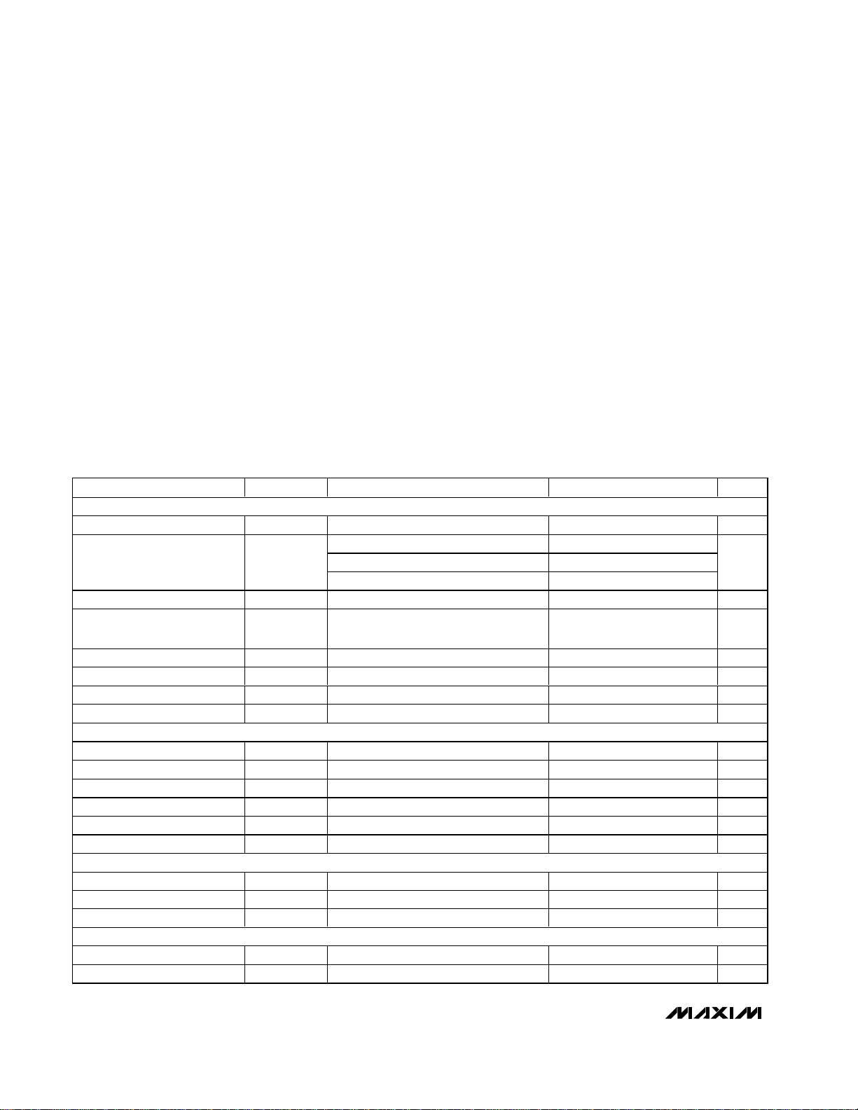
ABSOLUTE MAXIMUM RATINGS
ELECTRICAL CHARACTERISTICS
(AVDD= DVDD= 5V, external reference = 4.096V, C
REF
= 1µF, C
REFADJ
= 0.1µF, TA= T
MIN
to T
MAX
, unless otherwise noted.
Typical values are at T
A
= +25°C.)
Stresses beyond those listed under “Absolute Maximum Ratings” may cause permanent damage to the device. These are stress ratings only, and functional
operation of the device at these or any other conditions beyond those indicated in the operational sections of the specifications is not implied. Exposure to
absolute maximum rating conditions for extended periods may affect device reliability.
AVDDto AGND .........................................................-0.3V to +6V
DVDDto DGND.........................................................-0.3V to +6V
AGND to DGND.....................................................-0.3V to +0.3V
AIN, REF, REFADJ to AGND....................-0.3V to (AVDD+ 0.3V)
CS, HBEN, R/C, RESET to DGND ............................-0.3V to +6V
Digital Output (D13–D0, EOC)
to DGND ..................................................-0.3V to (DV
DD
+ 0.3V)
Maximum Continuous Current Into Any Pin ........................50mA
Continuous Power Dissipation (T
A
= +70°C)
20-Pin TSSOP (derate 10.9mW/°C above +70°C) .......879mW
28-Pin TSSOP (derate 12.8mW/°C above +70°C) .....1026mW
Operating Temperature Ranges
MAX106_ _CU_...................................................0°C to +70°C
MAX106_ _EU_ ................................................-40°C to +85°C
Storage Temperature Range .............................-65°C to +150°C
Junction Temperature......................................................+150°C
Lead Temperature (soldering, 10s) .................................+300°C
DC ACCURACY
Resolution N 14 Bits
Differential Nonlinearity DNL No missing codes over temperature ±1 LSB
Transition Noise
Offset Error 0.2 1 mV
Gain Error (Note 2) ±0.002 ±0.02 %FSR
Offset Drift 0.6 ppm/°C
Gain Drift 0.2 ppm/°C
DYNAMIC PERFORMANCE (f
Signal-to-Noise Plus Distortion SINAD 81 84 dB
Signal-to-Noise Ratio SNR 82 84 dB
Total Harmonic Distortion THD -99 -86 dB
Spurious-Free Dynamic Range SFDR 87 102 dB
Full-Power Bandwidth -3dB point 4 MHz
Full-Linear Bandwidth SINAD > 81dB 20 kHz
CONVERSION RATE
Sample Rate f
Aperture Delay 40 ns
Aperture Jitter 100 ps
ANALOG INPUT
Input Range V
Input Capacitance C
PARAMETER SYMBOL CONDITIONS MIN TYP MAX UNITS
IN(SINE-WAVE)
SAMPLE
AIN
AIN
MAX106_A
MAX106_B ±2Relative Accuracy (Note 1) INL
MAX106_C ±3
RMS noise, includes quantization
noise
= 1kHz, VIN = 4.096V
P-P
, 165ksps)
0V
±1
0.32
165 ksps
REF
40 pF
LSB
LSB
RMS
V
MAX1065/MAX1066
Low-Power, 14-Bit Analog-to-Digital Converters
with Parallel Interface
_______________________________________________________________________________________ 3
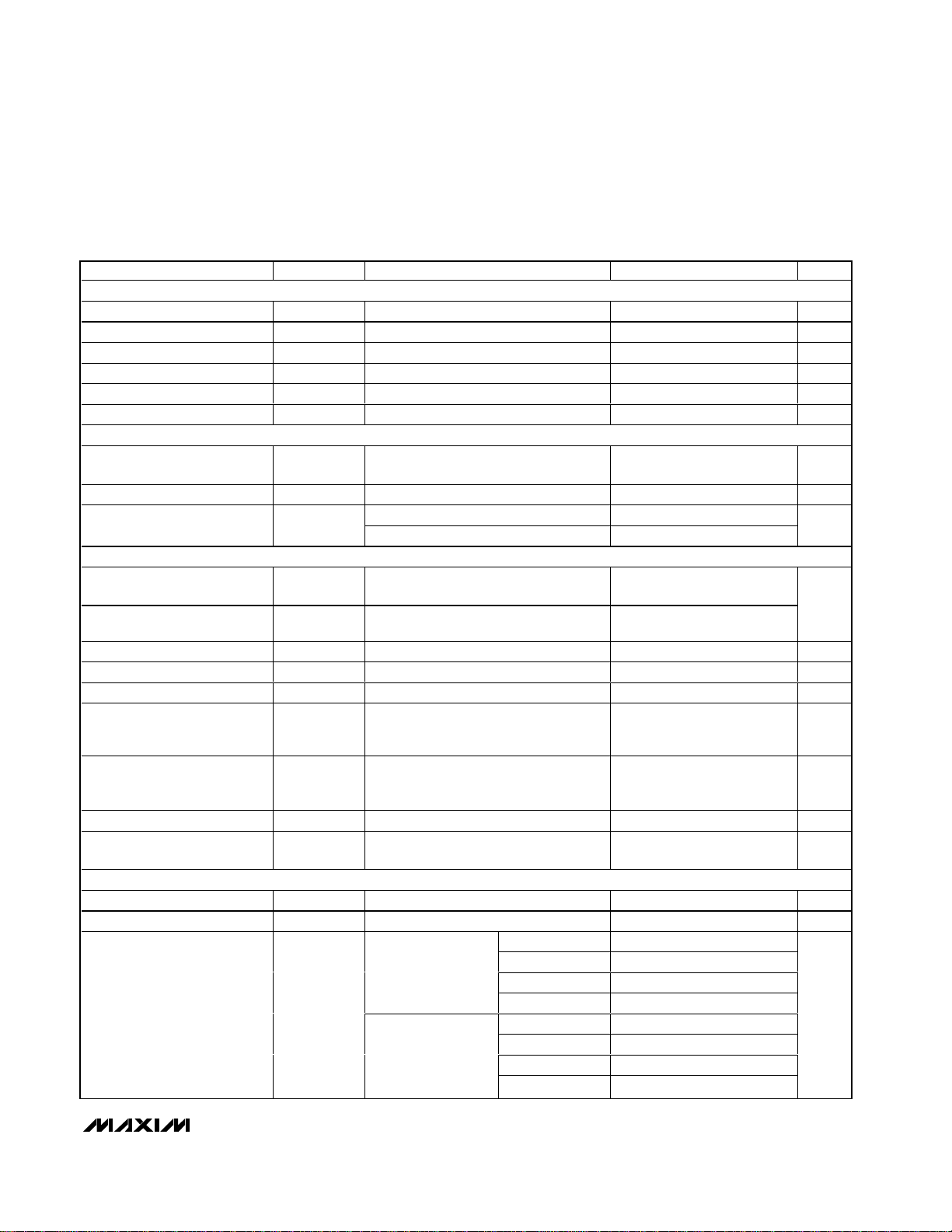
ELECTRICAL CHARACTERISTICS (continued)
(AVDD= DVDD= 5V, external reference = 4.096V, C
REF
= 1µF, C
REFADJ
= 0.1µF, TA= T
MIN
to T
MAX
, unless otherwise noted.
Typical values are at T
A
= +25°C.)
PARAMETER SYMBOL CONDITIONS MIN TYP MAX UNITS
INTERNAL REFERENCE
REF Output Voltage V
REF Output Tempco TC
REF Short-Circuit Current I
Capacitive Bypass at REFADJ C
Capacitive Bypass at REF C
REFADJ Input Leakage Current I
REF
REF
REFSC
REFADJ
REF
REFADJ
EXTERNAL REFERENCE
REFADJ Buffer Disable
Threshold
To power-down the internal reference
REF Input Voltage Range Internal reference disabled 3.8 AV
REF Input Current I
REF
V
Shutdown mode ±0.1
DIGITAL INPUTS/OUTPUTS (CS, R/C, EOC, D0–D13, RESET, HBEN)
Input High Voltage V
Input Low Voltage V
Input Leakage Current I
Input Hysteresis V
Input Capacitance C
Output High Voltage V
IH
IL
IN
HYST
IN
OH
V
I
SOURCE
DV
AV
I
SINK
Output Low Voltage V
OL
DV
AV
Three-State Leakage Current I
Three-State Output
Capacitance
OZ
C
OZ
D0–D13 ±0.1 ±10 µA
POWER REQUIREMENTS
Analog Supply Voltage AV
Digital Supply Voltage DV
DD
DD
Internal reference
Analog Supply Current I
AVDD
External reference
= 4.096V, f
REF
= 0 or DV
IH
= 0.5mA,
= 2.7V to 5.25V,
DD
= 5.25V
DD
= 1.6mA,
= 2.7V to 5.25V,
DD
= 5.25V
DD
DD
4.056 4.096 4.136 V
0.1 µF
1µF
AV
-
DD
0.4
= 165ksps 62 120
SAMPLE
0.7 x
DV
DD
-
D
VDD
0.4
4.75 5.25 V
2.7 AV
165ksps 2.7 3.2
100ksps 2.0
10ksps 1.0
1ksps 1.0
165ksps 1.8 2.3
100ksps 1.1
10ksps 0.1
1ksps 0.01
±35 ppm/°C
±10 mA
20 µA
±0.1 ±1 µA
0.1 V
15 pF
15 pF
AV
-
DD
0.1
DD
0.3 x
DV
DD
0.4 V
DD
V
V
µA
V
V
V
mA
MAX1065/MAX1066
Low-Power, 14-Bit Analog-to-Digital Converters
with Parallel Interface
4 _______________________________________________________________________________________
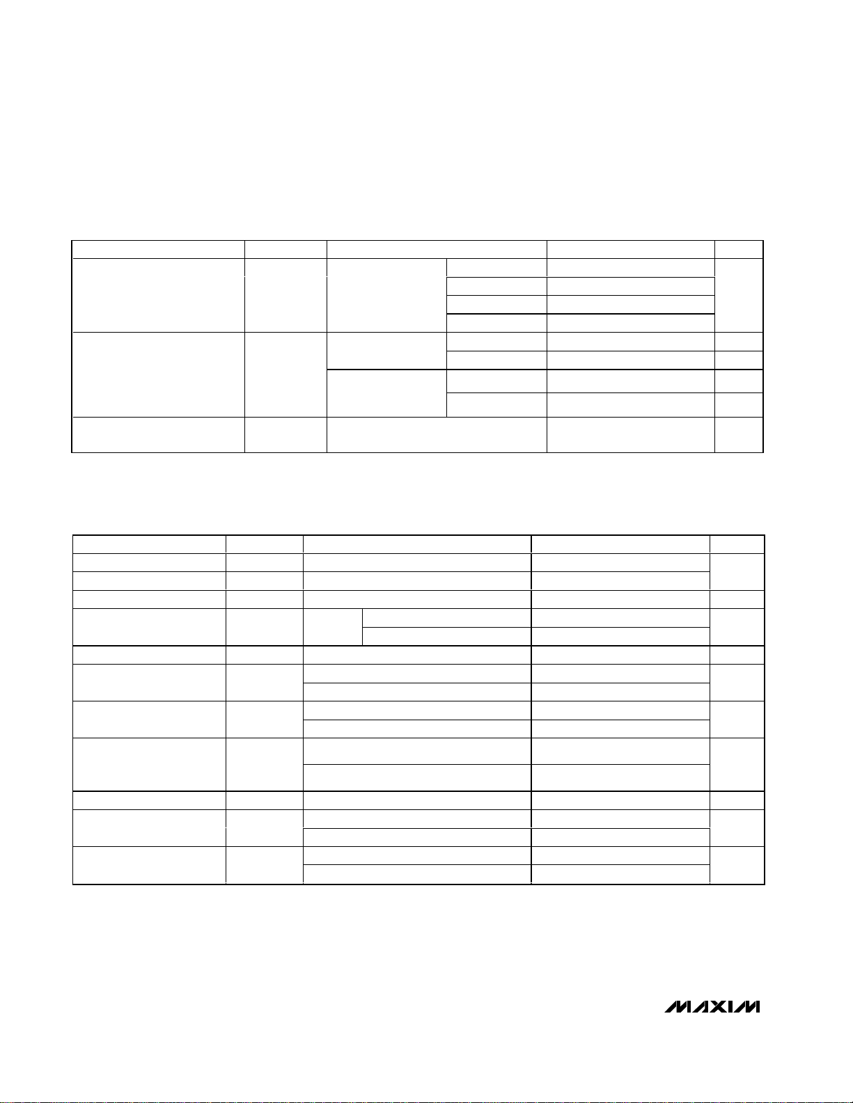
ELECTRICAL CHARACTERISTICS (continued)
(AVDD= DVDD= 5V, external reference = 4.096V, C
REF
= 1µF, C
REFADJ
= 0.1µF, TA= T
MIN
to T
MAX
, unless otherwise noted.
Typical values are at T
A
= +25°C.)
TIMING CHARACTERISTICS (Figures 1 and 2)
(AVDD= 4.75V to 5.25V, DVDD= 2.7V to AVDD, external reference = 4.096V, C
REF
= 1µF, C
REFADJ
= 0.1µF, C
D
13–D0,
C
EOC
= 20pF,
T
A
= T
MIN
to T
MAX
, unless otherwise noted. Typical values are at TA= +25°C.)
Note 1: Relative accuracy is the deviation of the analog value at any code from its theoretical value after offset and gain errors have
been removed.
Note 2: Offset nulled.
Note 3: Maximum specification is limited by automated test equipment.
Note 4: Defined as the change in positive full scale caused by a ±5% variation in the nominal supply.
Note 5: To ensure best performance, finish reading the data and wait t
BR
before starting a new acquisition.
PARAMETER SYMBOL CONDITIONS MIN TYP MAX UNITS
Digital Supply Current I
DVDD
D0–D13 = all zeros
Full power-down
Shutdown Supply Current
(Note 3)
I
SHDN
REF and REF
buffer enabled
(standby mode)
Power-Supply Rejection Ratio
(Note 4)
PSRR AV
165ksps 0.5 0.7
100ksps 0.3
10ksps 0.03
1ksps 0.003
I
AVDD
I
DVDD
I
AVDD
I
DVDD
= 5V, ±5%, full-scale input 68 dB
DD
0.05 5 mA
0.5 5 µA
1.0 1.2 mA
0.5 5 µA
PARAMETER SYMBOL CONDITIONS MIN TYP MAX UNITS
Acquisition Time t
Conversion Time t
CS Pulse Width High t
CS Pulse Width Low t
R/C to CS Fall Setup Time t
R/C to CS Fall Hold Time t
CS to Output Data Valid t
HBEN Transition To
Output Data Valid
(MAX1066 only)
EOC Fall To CS Fall t
CS Rise To EOC Rise t
Bus Relinquish Time
(Note 5)
ACQ
CONV
CSH
CSL
DO
t
DO1
EOC
t
DS
DH
DV
BR
(Note 5) 40 ns
V
= 4.75V to 5.25V 40
(Note 5)
V
DVDD
V
DVDD
V
DVDD
V
DVDD
V
DVDD
V
DVDD
V
DVDD
V
DVDD
V
DVDD
V
DVDD
DVDD
V
= 2.7V to 4.74V 60
DVDD
= 4.75V to 5.25V 40
= 2.7V to 5.25V 60
= 4.75V to 5.25V 40
= 2.7V to 4.74V 80
= 4.75V to 5.25V 40
= 2.7V to 4.74V 80
= 4.75V to 5.25V 40
= 2.7V to 4.74V 80
= 4.75V to 5.25V 40
= 2.7V to 4.74V 80
1.1
4.7
0ns
0ns
mA
µs
ns
ns
ns
ns
ns
ns
MAX1065/MAX1066
Low-Power, 14-Bit Analog-to-Digital Converters
with Parallel Interface
_______________________________________________________________________________________ 5
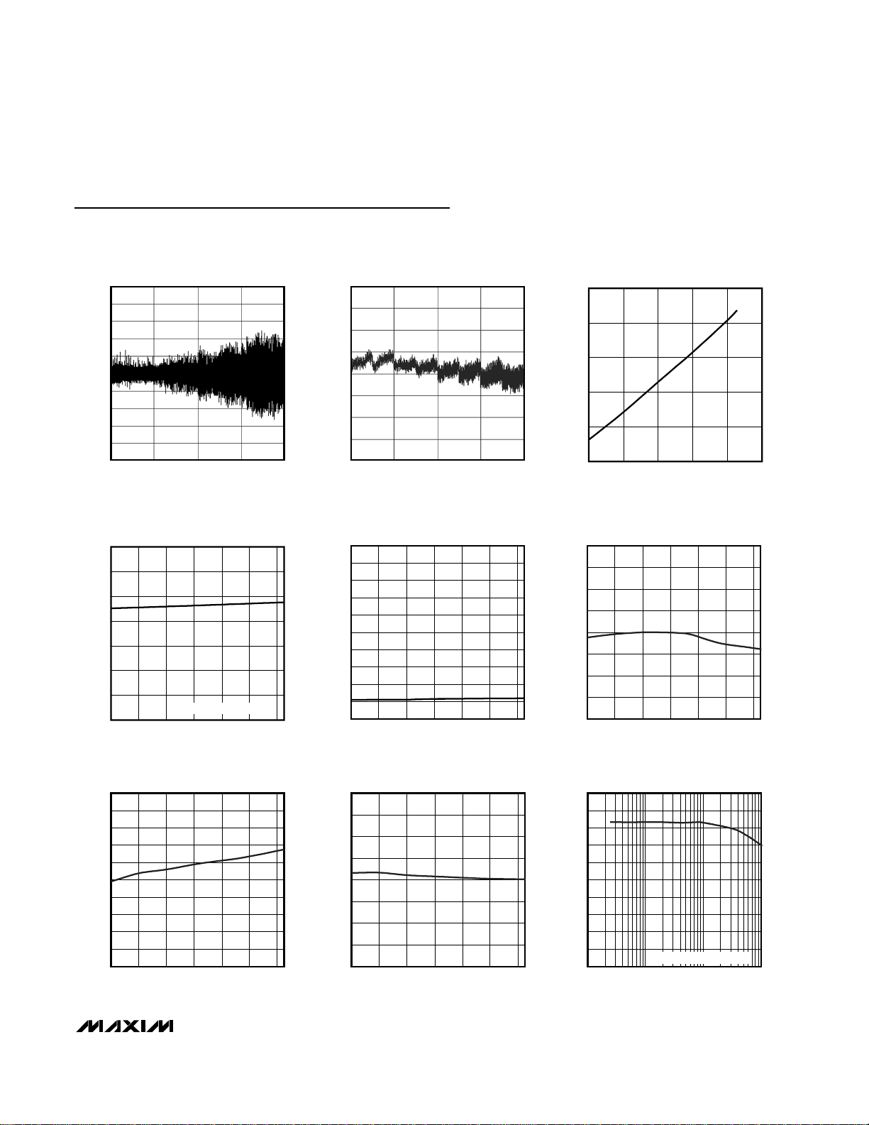
Typical Operating Characteristics
(AVDD= DVDD= 5V, external reference = 4.096V, C
REF
= 1µF, C
REFADJ
= 0.1µF, TA = +25°C, unless otherwise noted.)
DNL vs. OUTPUT CODE
1.0
0.8
0.6
0.4
0.2
0
DNL (LSB)
-0.2
-0.4
-0.6
-0.8
-1.0
0 16384
OUTPUT CODE
I
+ I
AVDD
SUPPLY CURRENT
DVDD
1228881924096
2.0
1.5
1.0
MAX1065/MAX1066 toc01
0.5
INL (LSB)
-0.5
-1.0
-1.5
-2.0
0
vs. TEMPERATURE
3.5
3.0
2.5
2.0
1.5
SUPPLY CURRENT (mA)
1.0
0.5
0
-40
SAMPLE RATE = 165ksps
806040200-20
TEMPERATURE (°C)
5.0
4.5
4.0
3.5
MAX1065/MAX1066 toc04
3.0
2.5
2.0
1.5
SHUTDOWN CURRENT (µA)
1.0
0.5
0
INL vs. OUTPUT CODE
0 16384
OUTPUT CODE
I
+ I
AVDD
DVDD
vs. TEMPERATURE
-40
TEMPERATURE (°C)
1228881924096
SHUTDOWN CURRENT
806040200-20
10
1
MAX1065/MAX1066 toc02
0.1
0.01
SUPPLY CURRENT (mA)
0.001
0.0001
0.01 1000
4.136
4.126
4.116
MAX1065/MAX1066 toc05
4.106
4.096
4.086
INTERNAL REFERENCE (V)
4.076
4.066
4.056
-40
I
+ I
AVDD
SUPPLY CURRENT
DVDD
vs. SAMPLE RATE
CONVERSION RATE (ksps)
INTERNAL REFERENCE
vs. TEMPERATURE
TEMPERATURE (°C)
MAX1065/MAX1066 toc03
1001010.1
MAX1065/MAX1066 toc06
806040200-20
OFFSET ERROR vs. TEMPERATURE
1000
800
600
400
200
0
-200
OFFSET ERROR (µV)
-400
-600
-800
0
-40
TEMPERATURE (°C)
SINAD vs. FREQUENCY
SAMPLE RATE = 165ksps
0.1 100
FREQUENCY (kHz)
101
MAX1065/MAX1066 toc07
806040200-20
0.020
GAIN ERROR vs. TEMPERATURE
0.015
0.010
0.005
0
-0.005
GAIN ERROR (%FSR)
-0.010
-0.015
-0.020
-40
TEMPERATURE (°C)
MAX1065/MAX1066 toc08
806040200-20
100
90
80
70
60
50
SINAD (dB)
40
30
20
10
0
MAX1065/MAX1066 toc09

MAX1065/MAX1066
Low-Power, 14-Bit Analog-to-Digital Converters
with Parallel Interface
6 _______________________________________________________________________________________
Typical Operating Characteristics (continued)
(AVDD= DVDD= 5V, external reference = 4.096V, C
REF
= 1µF, C
REFADJ
= 0.1µF, TA = +25°C, unless otherwise noted.)
TOTAL HARMONIC DISTORTION
vs. FREQUENCY
MAX1065/MAX1066 toc10
FREQUENCY (kHz)
THD (dB)
101
-100
-90
-80
-70
-60
-50
-40
-30
-20
-10
0
-110
0.1 100
SAMPLE RATE = 165ksps
SPURIOUS-FREE DYNAMIC RANGE
vs. FREQUENCY
MAX1065/MAX1066 toc11
FREQUENCY (kHz)
SFDR (dB)
101.0
10
20
30
40
50
60
70
80
90
100
110
0
0.1 100
SAMPLE RATE = 165ksps
FFT AT 1kHz
MAX1065/MAX1066 toc12
FREQUENCY (kHz)
MAGNITUDE (dB)
604020
-120
-100
-80
-60
-40
-20
0
-140
080
SAMPLE RATE = 165ksps
Pin Description
PIN NAME
MAX1065
FUNCTION
11D6
Three-State Digital Data Output
22D7
Three-State Digital Data Output. D13 is the MSB.
3 3 D8 D6/0 Three-State Digital Data Output
4 4 D9 D7/0 Three-State Digital Data Output
5 — D10 — Three-State Digital Data Output
6 — D11 — Three-State Digital Data Output
7 — D12 — Three-State Digital Data Output
8 — D13 — Three-State Digital Data Output (MSB)
95 R/C
Read/Convert Input. Power up and put the MAX1065/MAX1066 in acquisition
mode by holding R/C low during the first falling edge of CS. During the
second falling edge of CS the level on R/C determines whether the reference
and reference buffer power down or remain on after conversion. Set R/C high
during the second falling edge of CS to power down the reference and buffer,
or set R/C low to leave the reference and buffer powered up. Set R/C high
during the third falling edge of CS to put valid data on the bus.
10 6 EOC End Of Conversion. EOC drives low when conversion is complete.
11 7 AV
DD
Analog Supply Input. Bypass with a 0.1µF capacitor to AGND.
12 8 AGND Analog Ground. Primary analog ground (star ground).
13 9 AIN Analog Input
14 10 AGND
Analog Ground. Connect Pin 14 to Pin 12 (MAX1065). Connect Pin 10 to Pin 8
(MAX1066).
MAX1066 MAX1065 MAX1066
D4/D12
D5/D13

MAX1065/MAX1066
Low-Power, 14-Bit Analog-to-Digital Converters
with Parallel Interface
_______________________________________________________________________________________ 7
Pin Description (continued)
PIN NAME
MAX1065
FUNCTION
15 11 REFADJ
Reference Buffer Output. Bypass REFADJ with a 0.1µF capacitor to AGND for
internal reference mode. Connect REFADJ to AVDD to select external
reference mode.
16 12 REF
Reference Input/Output. Bypass REF with a 1µF capacitor to AGND for internal
reference mode. External reference input when in external reference mode.
17 — RESET Reset Input. Logic high resets the device.
— 13 HBEN
High Byte-Enable Input. Used to multiplex the 14-bit conversion result.
1: Most significant byte available on the data bus.
0: Least significant byte available on the data bus.
18 14 CS
Convert Start. The first falling edge of CS powers up the device and enables
acquire mode when R/C is low. The second falling edge of CS starts
conversion. The third falling edge of CS loads the result onto the bus when R/C
is high.
19 15 DGND Digital Ground
20 16 DV
DD
Digital Supply Voltage. Bypass with a 0.1µF capacitor to DGND.
21 17 N.C. D0/D8
No Connection. Do Not Connect (MAX1065).
Three-State Digital Data Output (MAX1066).
22 18 N.C. D1/D9
No Connection. Do Not Connect (MAX1065).
Three-State Digital Data Output (MAX1066).
23 19 D0
Three-State Digital Data Output
24 20 D1
Three-State Digital Data Output
25 — D2 — Three-State Digital Data Output
26 — D3 — Three-State Digital Data Output
27 — D4 — Three-State Digital Data Output
28 — D5 — Three-State Digital Data Output
REFERENCE
OUTPUT
REGISTERS
CLOCK
SUCCESSIVE-
APPROXIMATION
REGISTER AND
CONTROL LOGIC
CAPACITIVE
DAC
MAX1065
MAX1066
14 OR 8* 14 OR 8*
REFADJ
REF
DGNDAGND
RESET**
AIN
AV
DD
DV
DD
R/C
CS
EOC
HBEN*
AGND
D0–D13
OR
D0/D8–D5/D13*
*BYTE WIDE (MAX1066 ONLY)
**16-BIT WIDE (MAX1065 ONLY)
5kΩ
Functional Diagram
MAX1066 MAX1065 MAX1066
D2/D10
D3/D11

MAX1065/MAX1066
Detailed Description
Converter Operation
The MAX1065/MAX1066 use a successive-approximation
(SAR) conversion technique with an inherent track-andhold (T/H) stage to convert an analog input into a 14-bit
digital output. Parallel outputs provide a high-speed interface to most microprocessors (µPs). The Functional
Diagram shows a simplified internal architecture of the
MAX1065/MAX1066. Figure 3 shows a typical application
circuit for the MAX1066.
Analog Input
The equivalent input circuit is shown in Figure 4. A
switched capacitor digital-to-analog converter (DAC)
provides an inherent track-and-hold function. The single-ended input is connected between AIN and AGND.
Input Bandwidth
The ADC’s input-tracking circuitry has a 4MHz smallsignal bandwidth, so it is possible to digitize highspeed transient events and measure periodic signals
with bandwidths exceeding the ADC’s sampling rate by
using undersampling techniques. To avoid aliasing of
unwanted high-frequency signals into the frequency
band of interest, use antialias filtering.
Internal protection diodes, which clamp the analog
input to AVDDand/or AGND, allow the input to swing
from AGND - 0.3V to AVDD+ 0.3V, without damaging
the device.
If the analog input exceeds 300mV beyond the supplies, limit the input current to 10mA.
Track and Hold (T/H)
In track mode, the analog signal is acquired on the
internal hold capacitor. In hold mode, the T/H switches
open and the capacitive DAC samples the analog input.
Low-Power, 14-Bit Analog-to-Digital Converters
with Parallel Interface
8 _______________________________________________________________________________________
Figure 2. MAX1065/MAX1066 Timing Diagram
Figure 1. Load Circuits for D0–D13 Enable Time, CSto D0–D13
Delay Time and Bus Relinquish Time
D0–D13
C
OH,
OH,
AND
LOAD
= 20pF
1mA
DGND
a) HIGH-Z TO V
V
TO V
OL
V
TO HIGH-Z
OH
D0–D13
b) HIGH-Z TO V
V
OH
TO HIGH-Z
V
OL
1mA
TO V
OL,
DV
AND
DD
C
LOAD
DGND
OL,
= 20pF
t
CSH
t
ACQ
REF POWER-
DOWN BIT
t
DS
t
CONV
t
DV
t
DO
DATA VALID
t
DO1
HIGH/LOW
BYTE VALID
HIGH/LOW
BYTE VALID
t
EOC
t
BR
HI-Z
t
BR
EOC
D0–D13
HBEN*
D7/D13–D0/D8*
t
CSL
CS
R/C
t
DH
HI–Z
*HBEN AND BYTE-WIDE DATA BUS AVAILABLE ON MAX1066 ONLY.

During the acquisition, the analog input (AIN) charges
capacitor C
DAC
. The acquisition ends on the second
falling edge of CS. At this instant, the T/H switches
open. The retained charge on C
DAC
represents a
sample of the input.
In hold mode, the capacitive DAC adjusts during the
remainder of the conversion time to restore node ZERO
to zero within the limits of 14-bit resolution. At the end of
the conversion, force CS low to put valid data on the bus.
The time required for the T/H to acquire an input signal
is a function of how quickly its input capacitance is
charged. If the input signal’s source impedance is
high, the acquisition time lengthens and more time
must be allowed between conversions. The acquisition
time (t
ACQ
) is the maximum time the device takes to
acquire the signal. Use the following formula to calculate acquisition time:
t
ACQ
= 11(RS+ RIN) x 35pF
where R
IN
= 800Ω, RS= the input signal’s source
impedance, and t
ACQ
is never less than 1.1µs. A
source impedance less than 1kΩ does not significantly
affect the ADC’s performance.
To improve the input-signal bandwidth under AC conditions, drive AIN with a wideband buffer (>4MHz) that can
drive the ADC’s input capacitance and settle quickly.
Power-Down Modes
Select standby mode or shutdown mode with the R/C
bit during the second falling edge of CS (see Selecting
Standby or Shutdown Mode section). The MAX1065/
MAX1066 automatically enter either standby mode, reference and buffer on, or shutdown, reference and
buffer off, after each conversion depending on the status of R/C during the second falling edge of CS.
Internal Clock
The MAX1065/MAX1066 generate an internal conversion clock. This frees the microprocessor from the burden of running the SAR conversion clock. Total
conversion time after entering hold mode (second
falling edge of CS) to end-of-conversion (EOC) falling is
4.7µs (max).
Applications Information
Starting a Conversion
CS and R/C control acquisition and conversion in the
MAX1065/MAX1066 (Figure 2). The first falling edge of
CS powers up the device and puts it into acquisition
mode if R/C is low. The convert start is ignored if R/C is
high. When powering up from shutdown, the MAX1065/
MAX1066 needs at least 10ms (C
REFADJ
= 0.1µF, C
REF
= 1µF) for the internal reference to wake up and settle
before starting the conversion. The ADC may wake up
from shutdown to an unknown state. Put the ADC in a
known state by completing one “dummy” conversion.
The MAX1065/ MAX1066 will be in a known state, ready
for actual data acquisition, after the completion of the
dummy conversion. A dummy conversion consists of one
full conversion cycle.
The MAX1065 provides an alternative reset function to
reset the device (see RESET section).
Selecting Standby or Shutdown Mode
The MAX1065/MAX1066 have a selectable standby or
low-power shutdown mode. In standby mode, the
ADC’s internal reference and reference buffer do not
power down between conversions, eliminating the need
to wait for the reference to power up before performing
the next conversion. Shutdown mode powers down the
reference and reference buffer after completing a conversion. Supply current is greatly reduced when in
shutdown mode. The reference and reference buffer
require a minimum of 10ms (C
REFADJ
= 0.1µF, C
REF
=
1µF) to power up and settle from shutdown.
The state of R/C at the second falling edge of CS
selects which power-down mode the MAX1065/
MAX1066 enters upon conversion completion. Holding
R/C low causes the MAX1065/MAX1066 to enter standby mode. The reference and buffer are left on after the
conversion completes. R/C high causes the
MAX1065/MAX1066 to enter shutdown mode and shut
down the reference and buffer after conversion
(Figures 5 and 6).
When using an external reference, set the REF powerdown bit high for lowest current operation.
MAX1065/MAX1066
Low-Power, 14-Bit Analog-to-Digital Converters
with Parallel Interface
_______________________________________________________________________________________ 9
Figure 3. Typical Application Circuit for MAX1066
5V ANALOG 5V DIGITAL
0.1µF0.1µF
µP DATA
MAX1066
DV
DD
D0–D7 OR
D8–D13
EOC
REF
REFADJ
DGNDAGND
BUS
0.1µF1µF
AV
DD
ANALOG INPUT
HIGH
BYTE
LOW
BYTE
AIN
R/C
CS
HBEN

MAX1065/MAX1066
Standby Mode
While in standby mode, the supply current is reduced
to less than 1mA (typ). The next falling edge of CS with
R/C low causes the MAX1065/MAX1066 to exit standby
mode and begin acquisition. The reference and reference buffer remain active to allow quick turn-on time.
Standby mode allows significant power savings while
running at the maximum sample rate.
Shutdown Mode
In shutdown mode, the reference and reference buffer
are shut down between conversions. Shutdown mode
reduces supply current to 0.5µA (typ) immediately after
the conversion. The falling edge of CS with R/C low
causes the reference and buffer to wake up and enter
acquisition mode. To achieve 14-bit accuracy, allow
10ms (C
REFADJ
= 0.1µF, C
REF
= 1µF) for the internal
reference to wake up. Increase wakeup time proportionally when using larger values of C
REFADJ
and C
REF
.
Internal and External Reference
Internal Reference
The internal reference of the MAX1065/MAX1066 is
internally buffered to provide 4.096V (typ) output at
REF. Bypass REF to AGND and REFADJ to AGND with
1µF and 0.1µF respectively. Fine adjustments can be
made to the internal reference voltage by sinking or
sourcing current at REFADJ. The input impedance at
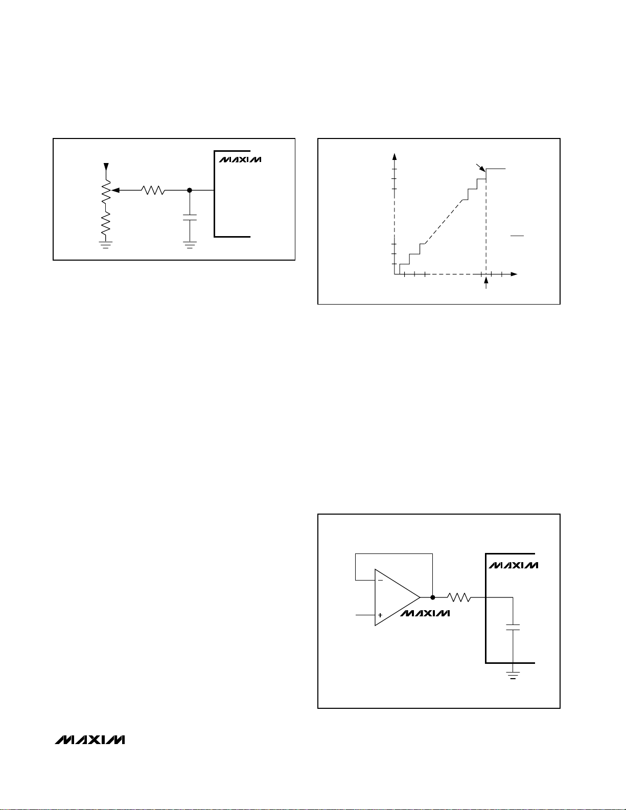
REFADJ is nominally 5kΩ. The internal reference voltage is adjustable to ±1.5% with the circuit of Figure 7.
External Reference
An external reference can be placed at either the input
(REFADJ) or the output (REF) of the MAX1065/
MAX1066’s internal buffer amplifier. When connecting
an external reference to REFADJ, the input impedance
is typically 5kΩ. Using the buffered REFADJ input
makes buffering the external reference unnecessary;
however, the internal buffer output must be bypassed
at REF with a 1µF capacitor.
Connect REFADJ to AVDDto disable the internal buffer.
Directly drive REF using an external reference. During
conversion, the external reference must be able to
drive 100µA of DC load current and have an output
impedance of 10Ω or less. REFADJ’s impedance is typically 5kΩ. The DC input impedance of REF is 40kΩ
minimum.
For optimal performance, buffer the reference through
an op amp and bypass REF with a 1µF capacitor.
Consider the MAX1065/MAX1066’s equivalent input
noise (80µV
RMS
) when choosing a reference.
Low-Power, 14-Bit Analog-to-Digital Converters
with Parallel Interface
10 ______________________________________________________________________________________
Figure 4. Equivalent Input Circuit
Figure 5. Selecting Standby Mode
Figure 6. Selecting Shutdown Mode
REF
AIN
C
SWITCH
TRACK
3pF
HOLD
CAPACITIVE DAC
AGND
C
= 32pF
DAC
HOLD TRACK
ZERO
R
IN
800Ω
AUTO-ZERO
RAIL
ACQUISITION CONVERSION
CS
REF POWERDOWN BIT
R/C
EOC
REF
AND
BUFFER
DATA
OUT
CS
R/C
EOC
REF
AND
BUFFER
ACQUISITION CONVERSION
REF POWERDOWN BIT
DATA
OUT
Reading the Conversion Result
EOC is provided to flag the microprocessor when a conversion is complete. The falling edge of EOC signals
that the data is valid and ready to be output to the bus.
D0–D13 are the parallel outputs of the MAX1065/
MAX1066. These three-state outputs allow for direct
connection to a microcontroller I/O bus. The outputs
remain high-impedance during acquisition and conversion. Data is loaded onto the bus with the third falling
edge of CS with R/C high after tDOns. Bringing CS high
forces the output bus back to high-impedance. The
MAX1065/MAX1066 then waits for the next falling edge
of CS to start the next conversion cycle (Figure 2).
The MAX1065 loads the conversion result onto a 14-bitwide data bus while the MAX1066 has a byte-wide output format. HBEN toggles the output between the
most/least significant byte. The least significant byte is
loaded onto the output bus when HBEN is low and the
most significant byte is on the bus when HBEN is high
(Figure 2).
RESET
Toggle RESET with CS high. The next falling edge of
CS will begin acquisition. This reset is an alternative to
the dummy conversion explained in the Starting a
Conversion section.
Transfer Function
Figure 8 shows the MAX1065/MAX1066 output transfer
function. The output is coded in standard binary.
Input Buffer
Most applications require an input buffer amplifier to
achieve 14-bit accuracy. If the input signal is multiplexed,
the input channel should be switched immediately after
acquisition, rather than near the end of or after a conversion. This allows more time for the input buffer amplifier to
respond to a large step-change in input signal. The input
amplifier must have a high enough slew rate to complete
the required output voltage change before the beginning
of the acquisition time. At the beginning of acquisition, the
internal sampling capacitor array connects to AIN (the
amplifier output) causing some output disturbance.
Ensure that the sampled voltage has settled to within the
required limits before the end of the acquisition time. If
the frequency of interest is low, AIN can be bypassed
with a large enough capacitor to charge the internal sampling capacitor with very little ripple. However, for AC use,
AIN must be driven by a wideband buffer (at least
10MHz), which must be stable with the ADC’s capacitive
load (in parallel with any AIN bypass capacitor used) and
also settle quickly. An example of this circuit using the
MAX4434 is given in Figure 9.
MAX1065/MAX1066
Low-Power, 14-Bit Analog-to-Digital Converters
with Parallel Interface
______________________________________________________________________________________ 11
Figure 7. MAX1065/MAX1066 Reference Adjust Circuit
Figure 9. MAX1065/MAX1066 Fast Settling Input Buffer
Figure 8. MAX1065/MAX1066 Transfer Function
5V
MAX1065
68kΩ
100kΩ
150kΩ
0.22µF
MAX1066
REFADJ
OUTPUT CODE
FULL-SCALE
11...111
11...110
11...101
00...011
00...010
00...001
00...000
0
123
INPUT VOLTAGE (LSB)
TRANSITION
FS - 3/2LSB
FS = V
1LSB =
FS
REF
V
16384
REF
MAX1065/
MAX1066
ANALOG
INPUT
MAX4434
10Ω
AIN
40pF

MAX1065/MAX1066
Layout, Grounding, and Bypassing
For best performance, use printed circuit boards. Do not
run analog and digital lines parallel to each other, and do
not lay out digital signal paths underneath the ADC package. Use separate analog and digital ground planes with
only one point connecting the two ground systems (analog and digital) as close to the device as possible.
Route digital signals far away from sensitive analog and
reference inputs. If digital lines must cross analog lines,
do so at right angles to minimize coupling digital noise
onto the analog lines. If the analog and digital sections
share the same supply, then isolate the digital and analog supply by connecting them with a low-value (10Ω)
resistor or ferrite bead.
The ADC is sensitive to high-frequency noise on the AV
DD
supply. Bypass AVDDto AGND with a 0.1µF capacitor in
parallel with a 1µF to 10µF low-ESR capacitor and the
smallest capacitor closest to the device. Keep capacitor
leads short to minimize stray inductance.
Definitions
Integral Nonlinearity
Integral nonlinearity (INL) is the deviation of the values
on an actual transfer function from a straight line. This
straight line can be either a best-straight-line fit or a line
drawn between the end points of the transfer function,
once offset and gain errors have been nullified. The
static linearity parameters for the MAX1065/MAX1066
are measured using the end-point method.
Differential Nonlinearity
Differential nonlinearity (DNL) is the difference between
an actual step width and the ideal value of 1LSB. A
DNL error specification of 1LSB guarantees no missing
codes and a monotonic transfer function.
Aperture Jitter and Delay
Aperture jitter is the sample-to-sample variation in the
time between samples. Aperture delay is the time
between the rising edge of the sampling clock and the
instant when the actual sample is taken.
Signal-to-Noise Ratio
For a waveform perfectly reconstructed from digital
samples, signal-to-noise ratio (SNR) is the ratio of the
full-scale analog input (RMS value) to the RMS quantization error (residual error). The ideal, theoretical minimum analog-to-digital noise is caused by quantization
noise error only and results directly from the ADC’s resolution (N-bits):
SNR = (6.02 x N + 1.76)dB
where N = 14 bits.
In reality, there are other noise sources besides quantization noise: thermal noise, reference noise, clock jitter,
etc. SNR is computed by taking the ratio of the RMS
signal to the RMS noise, which includes all spectral
components minus the fundamental, the first five harmonics, and the DC offset.
Signal-to-Noise Plus Distortion
Signal-to-noise plus distortion (SINAD) is the ratio of the
fundamental input frequency’s RMS amplitude to the
RMS equivalent of all the other ADC output signals.
Effective Number of Bits
Effective number of bits (ENOB) indicates the global
accuracy of an ADC at a specific input frequency and
sampling rate. An ideal ADC’s error consists of quantization noise only. With an input range equal to the fullscale range of the ADC, calculate the effective number
of bits as follows:
Total Harmonic Distortion
Total harmonic distortion (THD) is the ratio of the RMS
sum of the first five harmonics of the input signal to the
fundamental itself. This is expressed as:
where V1 is the fundamental amplitude and V2through
V5are the 2nd- through 5th-order harmonics.
Spurious-Free Dynamic Range
Spurious-free dynamic range (SFDR) is the ratio of the
RMS amplitude of the fundamental (maximum signal
component) to the RMS value of the next largest frequency component.
Chip Information
TRANSISTOR COUNT: 15,140
PROCESS: BiCMOS
Low-Power, 14-Bit Analog-to-Digital Converters
with Parallel Interface
12 ______________________________________________________________________________________
SINAD dB
( ) log
=×
20
Signal
RMS
Noise Distortion
()
+
RMS
ENOB
SINAD
=
602..
−
176
THD
=×
20
2
VVVV
2
log
2
+++
3
2
4
V
1
2
5
MAX1065/MAX1066
Low-Power, 14-Bit Analog-to-Digital Converters
with Parallel Interface
______________________________________________________________________________________ 13
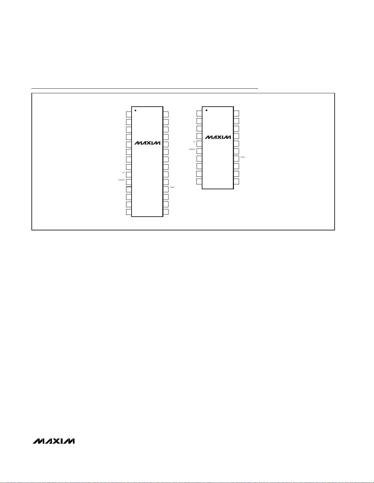
Pin Configurations
TOP VIEW
D6
D7
D8
D9
D10
D11
D12
D13
R/C
EOC
AV
DD
AGND
AIN
AGND
1
2
3
4
5
MAX1065
6
7
8
9
10
11
12
13
14
D5
28
2
D5/D13
D4
27
3
D3
26
D2
25
D1
24
D0
23
N.C.
22
N.C.
21
DV
20
19
DGND
18
CS
17
RESET
16
REF
REFADJ
15
D6/0
4
R/C
EOC
AV
AIN
DD
MAX1066
5
6
7
DD
8
9
10
TSSOP
1
D4/D12
20
D3/D11
19
D2/D10
18
D1/D9
17
D0/D8D7/0
16
DV
DD
DGND
15
14
CS
HBENAGND
13
12
REF
11
REFADJAGND
TSSOP

MAX1065/MAX1066
Low-Power, 14-Bit Analog-to-Digital Converters
with Parallel Interface
Maxim cannot assume responsibility for use of any circuitry other than circuitry entirely embodied in a Maxim product. No circuit patent licenses are
implied. Maxim reserves the right to change the circuitry and specifications without notice at any time.
14 ____________________Maxim Integrated Products, 120 San Gabriel Drive, Sunnyvale, CA 94086 408-737-7600
© 2002 Maxim Integrated Products Printed USA is a registered trademark of Maxim Integrated Products.
Package Information
TSSOP,NO PADS.EPS
 Loading...