

Page 1
General Description
The MAX1062 low-power, 14-bit analog-to-digital converter (ADC) features a successive approximation ADC,
automatic power-down, fast 1.1µs wake-up, and a highspeed SPI™/QSPI™/MICROWIRE™-compatible interface. The MAX1062 operates with a single +5V analog
supply and features a separate digital supply, allowing
direct interfacing with 2.7V to 5.25V digital logic.
At the maximum sampling rate of 200ksps, the
MAX1062 consumes only 2.5mA. Power consumption is
only 12.5mW (AVDD= DVDD= 5V) at a 200ksps (max)
sampling rate. AutoShutdown™ reduces supply current
to 130µA at 10ksps and to less than 10µA at reduced
sampling rates.
Excellent dynamic performance and low power, combined with ease of use and small package size (10-pin
µMAX) make the MAX1062 ideal for battery-powered
and data-acquisition applications or for other circuits
with demanding power consumption and space
requirements.
Applications
Motor Control
Industrial Process Control
Industrial I/O Modules
Data-Acquisition Systems
Thermocouple Measurements
Accelerometer Measurements
Portable- and Battery-Powered Equipment
Features
♦ 14-Bit Resolution, 1LSB DNL
♦ +5V Single-Supply Operation
♦ Adjustable Logic Level (2.7V to 5.25V)
♦ Input Voltage Range: 0 to V
REF
♦ Internal Track/Hold, 4MHz Input Bandwidth
♦ SPI/QSPI/MICROWIRE-Compatible Serial Interface
♦ Small 10-Pin µMAX Package
♦ Low Power
2.5mA at 200ksps
130µA at 10ksps
0.1µA in Power-Down Mode
MAX1062
14-Bit, +5V, 200ksps ADC with 10µA Shutdown
________________________________________________________________ Maxim Integrated Products 1
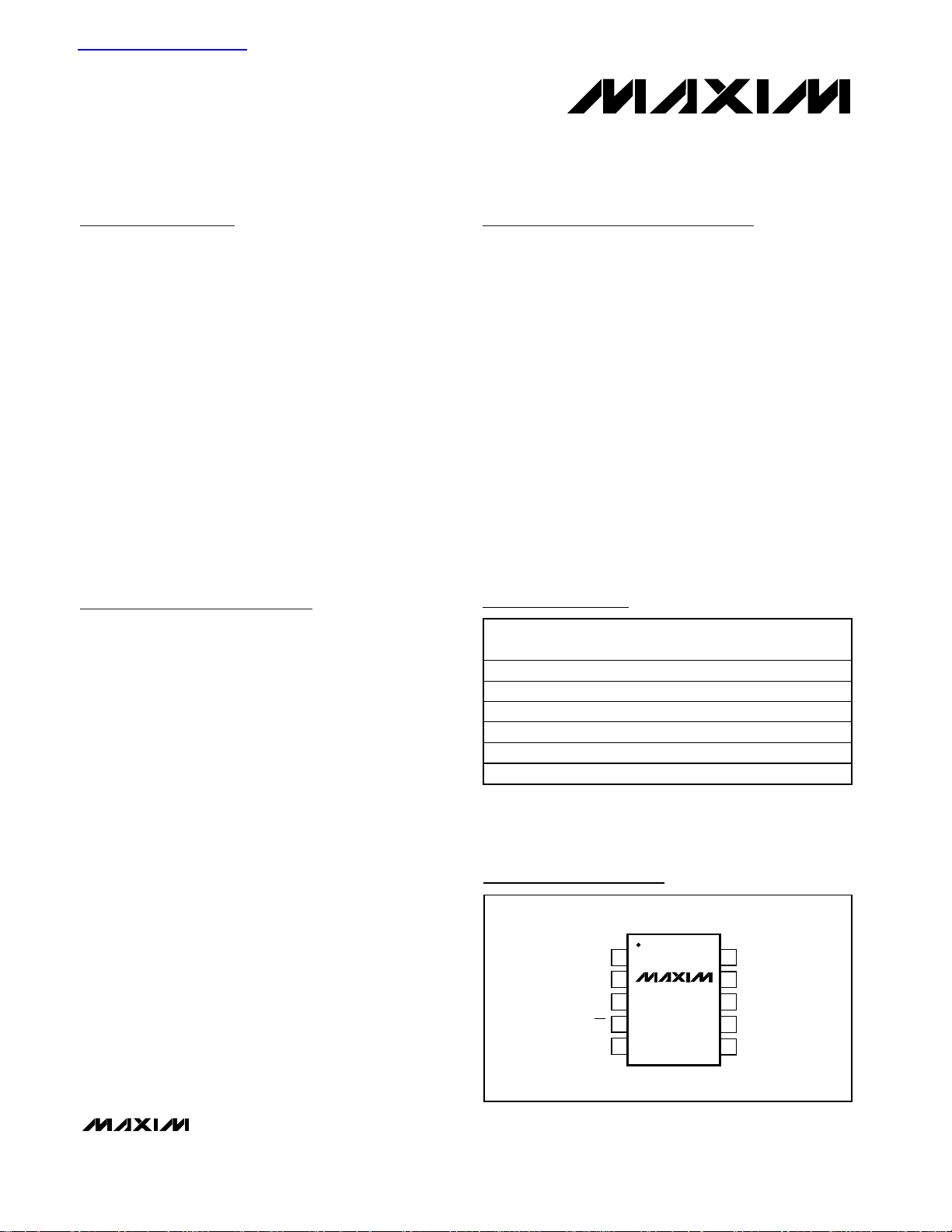
Pin Configuration
Ordering Information
19-2203; Rev 0; 10/01
Functional Diagram appears at end of data sheet.
For pricing, delivery, and ordering information, please contact Maxim/Dallas Direct! at
1-888-629-4642, or visit Maxim’s website at www.maxim-ic.com.
SPI and QSPI are trademarks of Motorola, Inc.
MICROWIRE is a trademark of National Semiconductor, Corp.
AutoShutdown is a trademark of Maxim Integrated Products, Inc.
查询MAX1062供应商
PART
MAX1062ACUB 0°C to 70°C 10 µMAX ±1
MAX1062BCUB 0°C to 70°C 10 µMAX ±2
MAX1062CCUB 0°C to 70°C 10 µMAX ±3
MAX1062AEUB -40°C to 85°C 10 µMAX ±1
MAX1062BEUB -40°C to 85°C 10 µMAX ±2
MAX1062CEUB -40°C to 85°C 10 µMAX ±3
TEMP.
RANGE
PINPACKAGE
INL
(LSB)
TOP VIEW
REF
AV
AGND
1
2
DD
MAX1062
3
4
5
µMAX
10
AIN
9
AGND
8
DV
DD
DGNDCS
7
DOUTSCLK
6
Page 2
MAX1062
14-Bit, +5V, 200ksps ADC with 10µA Shutdown
2 _______________________________________________________________________________________
ABSOLUTE MAXIMUM RATINGS
ELECTRICAL CHARACTERISTICS
(AVDD= DVDD= +4.75V to +5.25V, f
SCLK
= 4.8MHz (50% duty cycle), 24 clocks/conversion (200ksps), V
REF
= +4.096V, TA= T
MIN
to T
MAX
, unless otherwise noted. Typical values are at TA= +25°C.)
Stresses beyond those listed under “Absolute Maximum Ratings” may cause permanent damage to the device. These are stress ratings only, and functional
operation of the device at these or any other conditions beyond those indicated in the operational sections of the specifications is not implied. Exposure to
absolute maximum rating conditions for extended periods may affect device reliability.
AVDDto AGND ........................................................-0.3V to +6V
DV
DD
to DGND........................................................-0.3V to +6V
DGND to AGND....................................................-0.3V to +0.3V
AIN, REF to AGND ...................................-0.3V to (AV
DD
+ 0.3V)
SCLK, CS to DGND ..................................................-0.3V to +6V
DOUT to DGND .......................................-0.3V to (DV
DD
+ 0.3V)
Maximum Current Into Any Pin ...........................................50mA
Continuous Power Dissipation (T
A
= +70°C)
10-Pin µMAX (derate 5.6mW/°C above +70°C) ..........444mW
Operating Temperature Ranges
MAX1062_CUB .................................................0°C to +70°C
MAX1062_EUB ..............................................-40°C to +85°C
Maximum Junction Temperature .....................................+150°C
Storage Temperature Range .............................-65°C to +150°C
Lead Temperature (soldering, 10s) .................................+300°C
PARAMETER SYMBOL CONDITIONS MIN TYP MAX UNITS
DC ACCURACY (NOTE 1)
Resolution 14 Bits
Relative Accuracy (Note 2) INL
Differential Nonlinearity DNL No missing codes over temperature ±0.5 ±1 LSB
Transition Noise RMS noise ±0.32 LSB
Offset Error 0.2 1 mV
Gain Error (Note 3) ±0.002 ±0.01 %FSR
Offset Drift 0.4 ppm/oC
Gain Drift (Note 3) 0.2 ppm/oC
DYNAMIC SPECIFICATIONS (1kHz sine wave, 4.096Vp-p) (Note 1)
Signal-to-Noise Plus Distortion SINAD 81 84 dB
Signal-to-Noise Ratio SNR 82 84 dB
Total Harmonic Distortion THD -99 -86 dB
Spurious-Free Dynamic Range SFDR 87 101 dB
Full-Power Bandwidth -3dB point 4 MHz
Full-Linear Bandwidth SINAD > 81dB 20 kHz
CONVERSION RATE
Conversion Time (Note 4) t
Serial Clock Frequency f
Aperture Delay 15 ns
Aperture Jitter <50 ps
Sample Rate f
Track/Hold Acquisition Time t
MAX1062A ±1
MAX1062B ±2
MAX1062C ±3
CONV
SCLK
f
S
ACQ
/ 24 200 ksps
SCLK
5 240 µs
0.1 4.8 MHz
1.1 µs
LSB
RMS
Page 3
MAX1062
14-Bit, +5V, 200ksps ADC with 10µA Shutdown
_______________________________________________________________________________________ 3
ELECTRICAL CHARACTERISTICS (continued)
(AVDD= DVDD= +4.75V to +5.25V, f
SCLK
= 4.8MHz (50% duty cycle), 24 clocks/conversion (200ksps), V
REF
= +4.096V, TA= T
MIN
to T
MAX
, unless otherwise noted. Typical values are at TA= +25°C.)
PARAMETER SYMBOL CONDITIONS MIN TYP MAX UNITS
ANALOG INPUT (AIN)
Input Range V
Input Capacitance C
EXTERNAL REFERENCE
Input Voltage Range V
Input Current I
DIGITAL INPUTS (SCLK, CS)
Input High Voltage V
Input Low Voltage V
Input Leakage Current I
Input Hysteresis V
Input Capacitance C
DIGITAL OUTPUT (DOUT)
Output High Voltage V
Output Low Voltage V
Three-State Output Leakage
Current
Three-State Output Capacitance C
POWER SUPPLIES
Analog Supply AV
Digital Supply DV
Analog Supply Current I
Digital Supply Current I
AIN
AIN
REF
V
= 4.096V, f
REF
REF
V
= 4.096V, SCLK idle 0.01
REF
SCLK
CS = DVDD, SCLK idle 0.01
DVDD = +2.7V to +5.25V
IH
DVDD = +2.7V to +5.25V
IL
V
IN
HYST
IN
OH
OL
I
L
OUT
DD
DD
AVDD
= 0 to DV
IN
I
SOURCE
I
SINK
I
= 1.6mA, DVDD = +2.7V to +5.25V 0.4
SINK
CS = DV
CS = DV
DD
= 0.5mA, DVDD = +2.7V to +5.25V
= 10mA, DVDD = +4.75V to +5.25V 0.7
DD
DD
CS = DGND
CS = DGND,
DVDD
DOUT = all
zeros
0V
REF
40 pF
3.8 AV
= 4.8MHz 100
0.7 x
DV
DD
0.3 x
DV
±0.1 ±1 µA
0.2 V
15 pF
DV
-
DD
0.25V
±0.1 ±10 µA
15 pF
4.75 5.25 V
2.7 5.25 V
200ksps 2.0 2.5
100ksps 1.0
10ksps 0.1
1ksps 0.01
200ksps 0.6 1.0
100ksps 0.3
10ksps 0.03
1ksps 0.003
DD
DD
V
V
µA
V
V
V
V
mA
mA
Page 4
MAX1062
14-Bit, +5V, 200ksps ADC with 10µA Shutdown
4 _______________________________________________________________________________________
Note 1: AVDD= DVDD= +5V.
Note 2: Relative accuracy is the deviation of the analog value at any code from its theoretical value after the full-scale range has
been calibrated.
Note 3: Offset and reference errors nulled.
Note 4: Conversion time is defined as the number of clock cycles multiplied by the clock period; clock has 50% duty cycle.
Note 5: Defined as the change in positive full scale caused by a ±5% variation in the nominal supply voltage.
MAX1062 TIMING CHARACTERISTICS (Figures 1, 2, 3, and 6)
(AVDD= DVDD= +4.75V to +5.25V, f
SCLK
= 4.8MHz (50% duty cycle), 24 clocks/conversion (200ksps), V
REF
= +4.096V, TA= T
MIN
to T
MAX
, unless otherwise noted. Typical values are at TA= +25°C.)
(AVDD= +4.75V to +5.25V, DVDD= +2.7V to +5.25V, f
SCLK
= 4.8MHz (50% duty cycle), 24 clocks/conversion (200ksps), V
REF
=
+4.096V, T
A
= T
MIN
to T
MAX
, unless otherwise noted. Typical values are at TA= +25°C.)
ELECTRICAL CHARACTERISTICS (continued)
(AVDD= DVDD= +4.75V to +5.25V, f
SCLK
= 4.8MHz (50% duty cycle), 24 clocks/conversion (200ksps), V
REF
= +4.096V, TA= T
MIN
to T
MAX
, unless otherwise noted. Typical values are at TA= +25°C.)
PARAMETER SYMBOL CONDITIONS MIN TYP MAX UNITS
Shutdown Supply Current
Power-Supply Rejection Ratio
(Note 5)
I
+
AVDD
I
DVDD
PSRR
CS = DVDD, SCLK = idle 0.1 10 µA
AV
= DVDD = +4.75V to +5.25V, full-scale
DD
input
68 dB
PARAMETER SYMBOL CONDITIONS MIN TYP MAX UNITS
Acquisition Time t
SCLK to DOUT Valid t
CS Fall to DOUT Enable t
CS Rise to DOUT Disable t
CS Pulse Width t
CS Fall to SCLK Rise Setup t
CS Rise to SCLK Rise Hold t
SCLK High Pulse Width t
SCLK Low Pulse Width t
SCLK Period t
ACQ
C
DO
DV
TR
CSW
CSS
CSH
CH
CL
CP
= 50pF 50 ns
DOUT
C
= 50pF 80 ns
DOUT
C
= 50pF 80 ns
DOUT
1.1 µs
50 ns
100 ns
0ns
65 ns
65 ns
208 ns
PARAMETER SYMBOL CONDITIONS MIN TYP MAX UNITS
Acquisition Time t
SCLK to DOUT Valid t
CS Fall to DOUT Enable t
CS Rise to DOUT Disable t
CS Pulse Width t
CS Fall to SCLK Rise Setup t
CS Rise to SCLK Rise Hold t
SCLK High Pulse Width t
SCLK Low Pulse Width t
SCLK Period t
ACQ
DO
DV
TR
CSW
CSS
CSH
CH
CL
CP
C
C
C
DOUT
DOUT
DOUT
1.1 µs
= 50pF 100 ns
= 50pF 100 ns
= 50pF 80 ns
50 ns
100 ns
0ns
65 ns
65 ns
208 ns
Page 5
MAX1062
14-Bit, +5V, 200ksps ADC with 10µA Shutdown
_______________________________________________________________________________________ 5
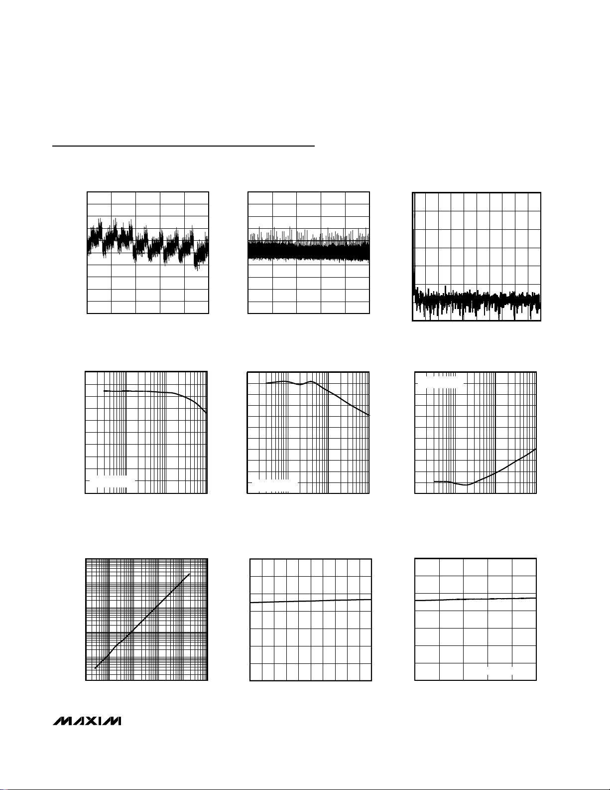
Typical Operating Characteristics
(AVDD= DVDD= +5V, f
SCLK
= 4.8MHz, C
LOAD
= 50pF, V
REF
= +4.096V, TA= 25°C, unless otherwise noted.)
INL vs. OUTPUT CODE
1.0
0.8
0.6
0.4
0.2
0
INL (LSB)
-0.2
-0.4
-0.6
-0.8
-1.0
0 16384
OUTPUT CODE
SINAD VS. FREQUENCY
100
90
80
70
60
50
SINAD (dB)
40
30
20
f
10
0
= 200kHz
SAMPLE
0.1 100101
FREQUENCY (kHz)
13107983065533276
MAX1062 toc01
MAX1062 toc04
1.0
0.8
0.6
0.4
0.2
0
DNL (LSB)
-0.2
-0.4
-0.6
-0.8
-1.0
0 16384
110
100
90
80
70
60
50
SFDR (dB)
40
30
20
10
0
0.1 100101
DNL vs. OUTPUT CODE
OUTPUT CODE
SFDR VS. FREQUENCY
f
= 200kHz
SAMPLE
FREQUENCY (kHz)
MAX1062 FFT
0
-20
MAX1062 toc02
-40
-60
-80
MAGNITUDE (dB)
-100
-120
13107983065533276
-140
04020 60 8010 5030 70 90 100
FREQUENCY (kHz)
THD VS. FREQUENCY
0
f
= 200kHz
SAMPLE
-10
-20
MAX1062 toc05
-30
-40
-50
-60
THD (dB)
-70
-80
-90
-100
-110
0.1 100101
FREQUENCY (kHz)
MAX1062 toc03
MAX1062 toc06
SUPPLY CURRENT
10
1
0.1
0.01
SUPPLY CURRENT (mA)
0.001
0.0001
0.01 0.1 1 10 100 1000
VS. CONVERSION RATE
CONVERSION RATE (kHz)
3.5
3.0
MAX1062 toc07
2.5
2.0
1.5
SUPPLY CURRENT (mA)
1.0
0.5
0
4.75 4.954.85 5.05 5.15 5.25
SUPPLY CURRENT
VS. SUPPLY VOLTAGE
SUPPLY VOLTAGE (V)
3.5
3.0
MAX1062 toc08
2.5
2.0
1.5
SUPPLY CURRENT (mA)
1.0
0.5
0
SUPPLY CURRENT VS. TEMPERATURE
MAX1062 toc09
AVDD = DVDD= +5V
-40 10-15 35 60 85
TEMPERATURE (°C)
Page 6
MAX1062
14-Bit, +5V, 200ksps ADC with 10µA Shutdown
6 _______________________________________________________________________________________
Typical Operating Characteristics (continued)
(AVDD= DVDD= +5V, f
SCLK
= 4.8MHz, C
LOAD
= 50pF, V
REF
= +4.096V, TA= 25°C, unless otherwise noted.)
0
4
2
8
6
12
10
14
18
16
20
4.75 4.85 4.95 5.05 5.15 5.25
MAX1062 toc10
SUPPLY VOLTAGE (V)
I
SHDN
(nA)
SHUTDOWN SUPPLY CURRENT
VS. SUPPLY VOLTAGE
0
150
100
50
200
250
300
350
400
450
-40 10-15 35 60 85
SHUTDOWN SUPPLY CURRENT
VS. TEMPERATURE
MAX1062 toc11
TEMPERATURE (°C)
I
SHDN
(nA)
AVDD = DVDD = +5V
-1000
-400
-600
-800
-200
0
200
400
600
800
1000
4.75 4.954.85 5.05 5.15 5.25
OFFSET ERROR
VS. ANALOG SUPPLY VOLTAGE
MAX1062 toc12
SUPPLY VOLTAGE (V)
OFFSET ERROR (µV)
-1000
-400
-600
-800
-200
0
200
400
600
800
1000
-40 10-15 35 60 85
OFFSET ERROR VS. TEMPERATURE
MAX1062 toc13
TEMPERATURE (°C)
OFFSET ERROR (µV)
-0.020
-0.015
-0.010
-0.005
0
0.005
0.010
0.015
0.020
4.75 4.85 4.95 5.05 5.15 5.25
GAIN ERROR
VS. ANALOG SUPPLY VOLTAGE
MAX1062 toc14
SUPPLY VOLTAGE (V)
GAIN ERROR (%)
-0.020
-0.015
-0.010
-0.005
0
0.005
0.010
0.015
0.020
-40 -15 10 35 60 85
GAIN ERROR VS. TEMPERATURE
MAX1062 toc15
TEMPERATURE (°C)
GAIN ERROR (%)
Page 7

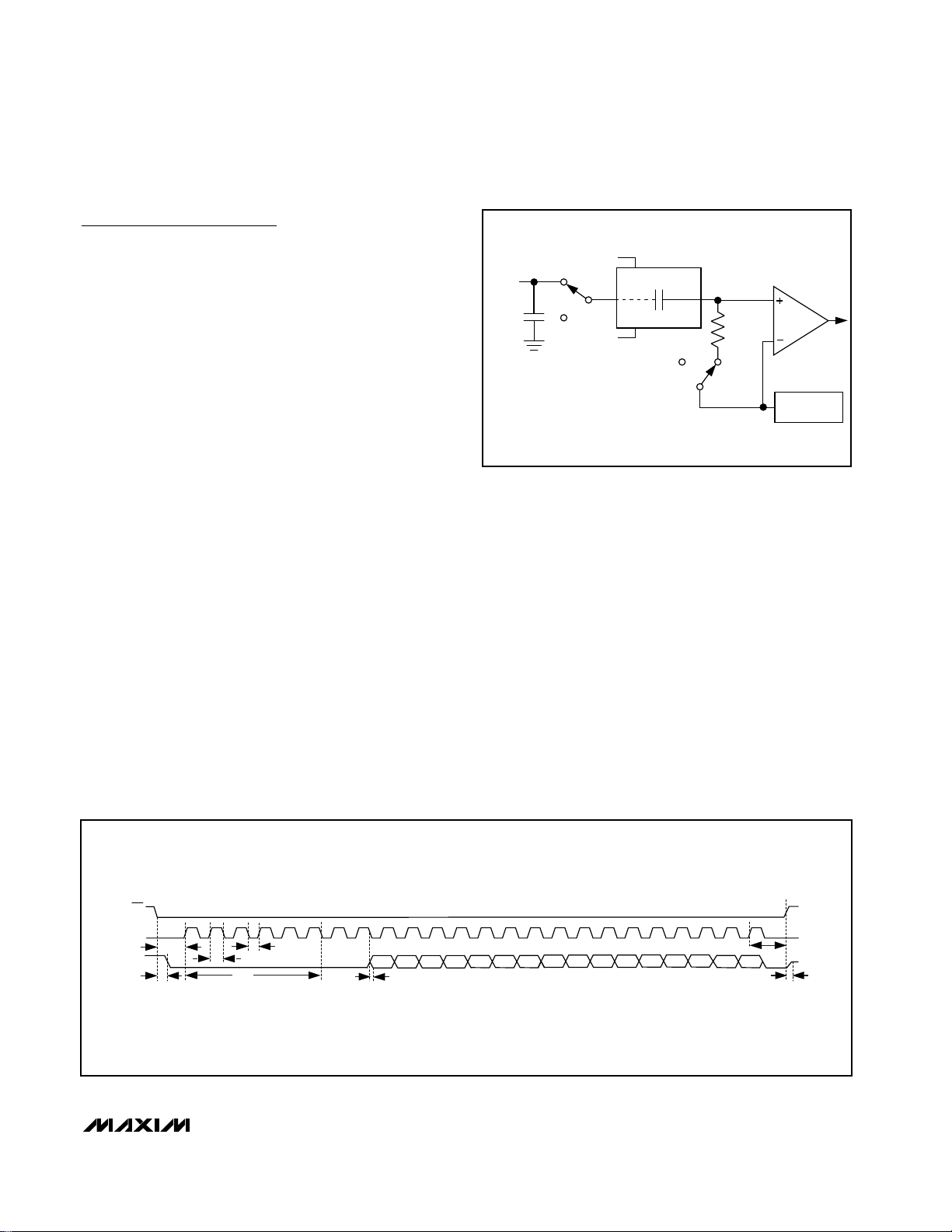
Detailed Description
The MAX1062 includes an input track-and-hold (T/H)
and successive-approximation register (SAR) circuitry
to convert an analog input signal to a digital 14-bit output. Figure 4 shows the MAX1062 in its simplest configuration. The serial interface requires only three digital
lines (SCLK, CS, and DOUT) and provides an easy
interface to microprocessors (µPs).
The MAX1062 has two power modes: normal and shutdown. Driving CS high places the MAX1062 in shutdown, reducing the supply current to 0.1µA (typ), while
pulling CS low places the MAX1062 in normal operating
mode. Falling edges on CS initiate conversions that are
driven by SCLK. The conversion result is available at
DOUT in unipolar serial format. The serial data stream
consists of eight zeros followed by the data bits (MSB
first). Figure 3 shows the interface-timing diagram.
Analog Input
Figure 5 illustrates the input sampling architecture of
the ADC. The voltage applied at REF sets the full-scale
input voltage.
Track-and-Hold (T/H)
In track mode, the analog signal is acquired on the
internal hold capacitor. In hold mode, the T/H switches
open and the capacitive DAC samples the analog
input.
During the acquisition, the analog input (AIN) charges
capacitor C
DAC
. The acquisition interval ends on the
falling edge of the sixth clock cycle (Figure 6). At this
instant, the T/H switches open. The retained charge on
C
DAC
represents a sample of the input.
In hold mode, the capacitive digital-to-analog converter
(DAC) adjusts during the remainder of the conversion
cycle to restore node ZERO to zero within the limits of
14-bit resolution. At the end of the conversion, force CS
high and then low to reset the input side of the C
DAC
switches back to AIN, and charge C
DAC
to the input
signal again.
The time required for the T/H to acquire an input signal
is a function of how quickly its input capacitance is
charged. If the input signal’s source impedance is high,
the acquisition time lengthens and more time must be
allowed between conversions. The acquisition time
(t
ACQ
) is the maximum time the device takes to acquire
the signal. Use the following formula to calculate acquisition time:
t
ACQ
= 11(RS+ RIN) x 35pF
where RIN= 800Ω, RS= the input signal’s source
impedance, and t
ACQ
is never less than 1.1µs. A
source impedance less than 1kΩ does not significantly
affect the ADC’s performance.
To improve the input signal bandwidth under AC conditions, drive AIN with a wideband buffer (>4MHz) that
can drive the ADC’s input capacitance and settle
quickly.
MAX1062
14-Bit, +5V, 200ksps ADC with 10µA Shutdown
_______________________________________________________________________________________ 7
Pin Description
PIN NAME FUNCTION
1 REF
2AVDDAnalog +5V Supply Voltage. Bypass to AGND (pin 3) with a 0.1µF capacitor.
3, 9 AGND Analog Ground. Connect pins 3 and 9 together. Place star ground at pin 3.
4 CS
5 SCLK
6 DOUT
7 DGND Digital Ground
8DVDDDigital Supply Voltage. Bypass to DGND with a 0.1µF capacitor.
10 AIN Analog Input
External Reference Voltage Input. Sets the analog voltage range. Bypass to AGND with a 4.7µF
capacitor.
Active Low Chip Select Input. Forcing CS high places the MAX1062 in shutdown with a typical
current of 0.1µA. A high-to-low transition on CS activates normal operating mode and initiates a
conversion.
Serial Clock Input. SCLK drives the conversion process and clocks out data at data rates up to
4.8MHz.
Serial Data Output. Data changes state on SCLK’s falling edge. DOUT is high impedance when CS
is high.
Page 8

MAX1062
Input Bandwidth
The ADC’s input tracking circuitry has a 4MHz smallsignal bandwidth, so it is possible to digitize highspeed transient events and measure periodic signals
with bandwidths exceeding the ADC’s sampling rate by
using undersampling techniques. To avoid aliasing of
unwanted high-frequency signals into the frequency
band of interest, use antialias filtering.
Analog Input Protection
Internal protection diodes, which clamp the analog
input to AV
DD
and/or AGND, allow the input to swing
from AGND - 0.3V to AVDD+ 0.3V, without damaging
the device.
If the analog input exceeds 300mV beyond the supplies, limit the input current to 10mA.
14-Bit, +5V, 200ksps ADC with 10µA Shutdown
8 _______________________________________________________________________________________
Figure 3. Detailed Serial Interface Timing
Figure 4. Typical Operating Circuit
Figure 1. Load Circuits for DOUT Enable Time and SCLK to
DOUT Delay Time
Figure 2. Load Circuits for DOUT Disable Time
V
DD
1mA
DOUT
1mA
DGND DGND
a) V
TO V
OL
C
LOAD
OH
DOUT
= 50pF C
b) HIGH-Z TO VOL AND VOH TO V
CS
t
CSS
SCLK
t
DOUT
DV
LOAD
= 50pF
t
CL
V
DD
1mA
DOUT
1mA
DGND DGND
OL
a) V
OH
C
LOAD
TO HIGH-Z b) VOL TO HIGH-Z
DOUT
= 50pF C
LOAD
= 50pF
t
CSW
t
CH
t
CP
t
DO
t
CSH
t
TR
V
AIN
REF
+5V
+5V
4.7µF
0.1µF
0.1µF
REF
AV
DV
AIN
DD
DD
MAX1062
GND
SCLK
DOUT
AGND
DGND
CS
CS
SCLK
DOUT
Page 9
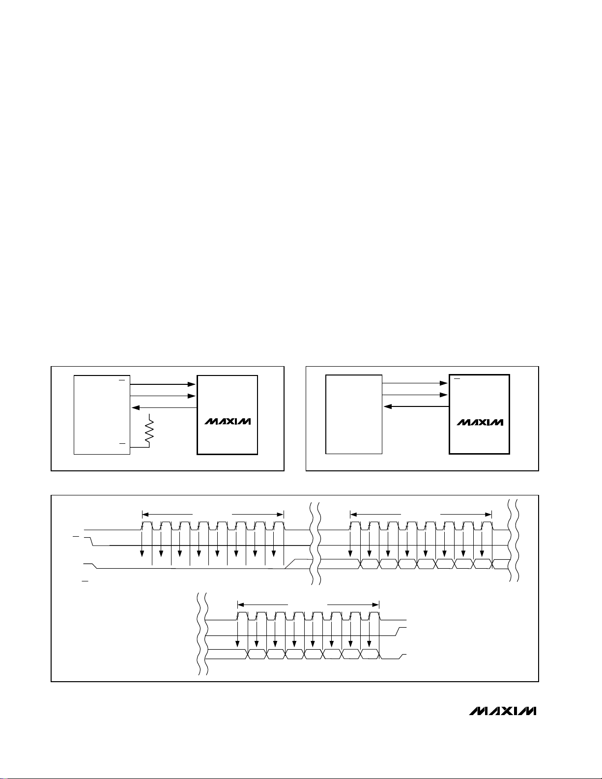
Digital Interface
Initialization after Power-Up and
Starting a Conversion
The digital interface consists of two inputs, SCLK and
CS, and one output, DOUT. A logic high on CS places
the MAX1062 in shutdown (autoshutdown) and places
DOUT in a high-impedance state. A logic low on CS
places the MAX1062 in the fully powered mode.
To start a conversion, pull CS low. A falling edge on CS
initiates an acquisition. SCLK drives the A/D conversion
and shifts out the conversion results (MSB first) at
DOUT.
Timing and Control
Conversion-start and data-read operations are controlled by the CS and SCLK digital inputs (Figures 6
and 7). Ensure that the duty cycle on SCLK is between
40% and 60% at 4.8MHz (the maximum clock frequency). For lower clock frequencies, ensure that the minimum high and low times are at least 65ns.
Conversions with SCLK rates less than 100kHz may
result in reduced accuracy due to leakage.
Note: Coupling between SCLK and the analog inputs
(AIN and REF) may result in an offset. Variations in frequency, duty cycle, or other aspects of the clock signal’s shape result in changing offset.
A CS falling edge initiates an acquisition sequence.
The analog input is stored in the capacitive DAC,
DOUT changes from high impedance to logic low, and
the ADC begins to convert after the sixth clock cycle.
SCLK drives the conversion process and shifts out the
conversion result on DOUT.
SCLK begins shifting out the data (MSB first) after the
falling edge of the 8th SCLK pulse. Twenty-four falling
clock edges are needed to shift out the eight leading
zeros, 14 data bits, and 2 sub-bits (S1 and S0). Extra
clock pulses occurring after the conversion result has
been clocked out, and prior to the rising edge of CS,
produce trailing zeros at DOUT and have no effect on
the converter operation.
Force CS high after reading the conversion’s LSB to
reset the internal registers and place the MAX1062 in
shutdown. For maximum throughput, force CS low
again to initiate the next conversion immediately after
the specified minimum time (t
CSW
).
Note: Forcing CS high in the middle of a conversion
immediately aborts the conversion and places the
MAX1062 in shutdown.
MAX1062
14-Bit, +5V, 200ksps ADC with 10µA Shutdown
_______________________________________________________________________________________ 9
Figure 5. Equivalent Input Circuit
Figure 6. External Timing Diagram
C
SWITCH
AIN
TRACK
3pF
HOLD
REF
CAPACITIVE DAC
GND
ZERO
C
32pF
DAC
HOLD
R
IN
800Ω
TRACK
AUTOZERO
RAIL
CS
SCLK
t
DOUT
t
DN
CSS
t
CH
t
ACQ
t
CL
D13 D12 D11
t
DO
1214 86
D10 D9 D8 D7
2016
24
t
CSH
S1 S0D6 D3 D2 D1 D0D5 D4
t
TR
Page 10

MAX1062
Output Coding and
Transfer Function
The data output from the MAX1062 is binary and Figure
8 depicts the nominal transfer function. Code transitions
occur halfway between successive-integer LSB values
(V
REF
= 4.096V and 1LSB = 250µV or 4.096V/16384).
Applications Information
External Reference
The MAX1062 requires an external reference with a
voltage range between 3.8V and AV
DD
. Connect the
external reference directly to REF. Bypass REF to
AGND (pin 3) with a 4.7µF capacitor. When not using a
low ESR bypass capacitor, use a 0.1µF ceramic capacitor in parallel with the 4.7µF capacitor. Noise on the
reference degrades conversion accuracy.
The input impedance at REF is 40kΩ for DC currents.
During a conversion the external reference at REF must
deliver 100µA of DC load current and have an output
impedance of 10Ω or less.
For optimal performance, buffer the reference through
an op amp and bypass the REF input. Consider the
MAX1062’s equivalent input noise (80µV
RMS
) when
choosing a reference.
Input Buffer
Most applications require an input buffer amplifier to
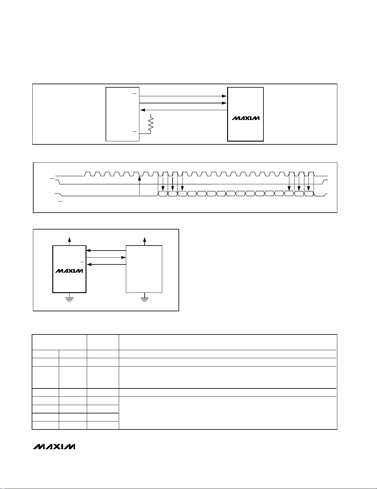
achieve 14-bit accuracy. If the input signal is multiplexed, switch the input channel immediately after acquisition, rather than near the end of or after a conversion
(Figure 9). This allows the maximum time for the input
buffer amplifier to respond to a large step change in the
input signal. The input amplifier must have a slew rate of
at least 2V/µs to complete the required output voltage
change before the beginning of the acquisition time.
At the beginning of the acquisition, the internal sampling
capacitor array connects to AIN (the amplifier output),
causing some output disturbance. Ensure that the sampled voltage has settled before the end of the acquisition
time.
Digital Noise
Digital noise can couple to AIN and REF. The conversion clock (SCLK) and other digital signals active during input acquisition contribute noise to the conversion
result. Noise signals synchronous with the sampling
interval result in an effective input offset. Asynchronous
signals produce random noise on the input, whose
14-Bit, +5V, 200ksps ADC with 10µA Shutdown
10 ______________________________________________________________________________________
Figure 7. Shutdown Sequence
Figure 8. Unipolar Transfer Function, Full Scale (FS) = V
REF
,
Zero Scale (ZS) = GND
COMPLETE CONVERSION SEQUENCE
CS
DOUT
CONVERSION 0
CONVERSION 1
POWERED UPPOWERED UP POWERED DOWN
OUTPUT CODE
FULL-SCALE
11 . . . 111
11 . . . 110
11 . . . 101
00 . . . 011
00 . . . 010
00 . . . 001
00 . . . 000
0
123
INPUT VOLTAGE (LSB)
TRANSITION
FS = V
FS - 3/2LSB
1LSB =
FS
REF
V
16384
REF
Page 11

high-frequency components may be aliased into the
frequency band of interest. Minimize noise by presenting a low impedance (at the frequencies contained in
the noise signal) at the inputs. This requires bypassing
AIN to AGND, or buffering the input with an amplifier
that has a small-signal bandwidth of several MHz, or
preferably both. AIN has about 4MHz of bandwidth.
Distortion
Avoid degrading dynamic performance by choosing an
amplifier with distortion much less than the MAX1062’s
total harmonic distortion (THD = -99dB at 1kHz) at frequencies of interest. If the chosen amplifier has insufficient common-mode rejection, which results in
degraded THD performance, use the inverting configuration (positive input grounded) to eliminate errors from
this source. Low temperature-coefficient, gain-setting
resistors reduce linearity errors caused by resistance
changes due to self-heating. To reduce linearity errors
due to finite amplifier gain, use amplifier circuits with
sufficient loop gain at the frequencies of interest.
DC Accuracy
To improve DC accuracy, choose a buffer with an offset
much less than the MAX1062’s offset (1mV (max) for +5V
supply), or whose offset can be trimmed while maintaining stability over the required temperature range.
Serial Interfaces
The MAX1062’s interface is fully compatible with SPI,
QSPI, and MICROWIRE standard serial interfaces.
If a serial interface is available, establish the CPU’s serial interface as master, so that the CPU generates the
serial clock for the MAX1062. Select a clock frequency
between 100kHz and 4.8MHz:
1) Use a general-purpose I/O line on the CPU to pull
CS low.
2) Activate SCLK for a minimum of 24 clock cycles.
The serial data stream of eight leading zeros followed by the MSB of the conversion result begins at
the falling edge of CS. DOUT transitions on SCLK’s
falling edge and the output is available in MSB-first
MAX1062
14-Bit, +5V, 200ksps ADC with 10µA Shutdown
______________________________________________________________________________________ 11
Figure 9. Change Multiplexer Input Near Beginning of Conversion to Allow Time for Slewing and Settling
A0 A1
IN1
IN2
4-TO-1
CLK
MUX
IN3
IN4
CS
A0
OUT
CONVERSION
MAX1062
AIN
CS
ACQUISITION
A1
CHANGE MUX INPUT HERE
Page 12
MAX1062
format. Observe the SCLK to DOUT valid timing
characteristic. Clock data into the µP on SCLK’s rising edge.
3) Pull CS high at or after the 24th falling clock edge. If
CS remains low, trailing zeros are clocked out after
the 2 sub-bits, S1 and S0.
4) With CS high, wait at least 50ns (t
CSW
) before start-
ing a new conversion by pulling CS low. A conversion can be aborted by pulling CS high before the
conversion ends. Wait at least 50ns before starting a
new conversion.
Data can be output in three 8-bit sequences or continuously. The bytes contain the results of the conversion
padded with eight leading zeros before the MSB. If the
serial clock has not been idled after the sub-bits (S1
and S0) and CS has been kept low, DOUT sends trailing zeros.
SPI and MICROWIRE Interfaces
When using the SPI (Figure 10a) or MICROWIRE
(Figure 10b) interfaces, set CPOL = 0 and CPHA = 0.
Conversion begins with a falling edge on CS (Figure
10c). Three consecutive 8-bit readings are necessary
to obtain the entire 14-bit result from the ADC. DOUT
data transitions on the serial clock’s falling edge. The
first 8-bit data stream contains all leading zeros. The
second 8-bit data stream contains the MSB through D6.
The third 8-bit data stream contains D5 through D0 followed by S1 and S0.
QSPI Interface
Using the high-speed QSPI interface with CPOL = 0
and CPHA = 0, the MAX1062 supports a maximum
f
SCLK
of 4.8MHz. Figure 11a shows the MAX1062 connected to a QSPI master and Figure 11b shows the
associated interface timing.
14-Bit, +5V, 200ksps ADC with 10µA Shutdown
12 ______________________________________________________________________________________
Figure 10a. SPI Connections
Figure 10b. MICROWIRE Connections
Figure 10c. SPI/MICROWIRE Interface Timing Sequence (CPOL = CPHA =0)
CS
SCLK
DOUT
MAX1062
SPI
SCK
MISO
I/O
V
DD
SS
CS
SCLK
DOUT
MAX1062
MICROWIRE
I/O
SK
SI
1ST BYTE READ
SCLK
CS
DOUT*
*WHEN CS IS HIGH, DOUT = HIGH-Z
641
00 0 000 00
8
D13 D12 D11 D10 D9 D8 D7 D6 D5
MSB
3RD BYTE READ
2420
S1 S0D5 D4 D3 D2 D1 D0
LSB
2ND BYTE READ
HIGH-Z
1612
Page 13
PIC16 with SSP Module and
PIC17 Interface
The MAX1062 is compatible with a PIC16/PIC17 microcontroller (µC) using the synchronous serial-port (SSP)
module.
To establish SPI communication, connect the controller
as shown in Figure 12a. Configure the PIC16/PIC17 as
system master, by initializing its synchronous serial-port
control register (SSPCON) and synchronous serial-port
status register (SSPSTAT) to the bit patterns shown in
Tables 1 and 2.
In SPI mode, the PIC16/PIC17 µC allows 8 bits of data
to be synchronously transmitted and received simulta-
MAX1062
14-Bit, +5V, 200ksps ADC with 10µA Shutdown
______________________________________________________________________________________ 13
Figure 11a. QSPI Connections
Figure 12a. SPI Interface Connection for a PIC16/PIC17
Figure 11b. QSPI Interface Timing Sequence (CPOL = CPHA = 0)
Table 1. Detailed SSPCON Register Contents
X = Don’t care
CS
SCK
MISO
QSPI
SS
V
DD
SCLK
CS
END OF
DOUT*
*WHEN CS IS HIGH, DOUT = HIGH-Z
ACQUISITION
D13 D12 D11
MSB
SCK
SDI
I/O
V
DD
PIC16/17
V
DD
SCLK
DOUT
CS
MAX1062
GND
CS
SCLK
DOUT
MAX1062
S1 S0
24
HIGH-Z
1214 86
D10 D9 D8 D7
2016
D6 D3 D2 D1
D5 D4
D0
LSB
CONTROL BIT
MAX1062
SETTINGS
SYNCHRONOUS SERIAL-PORT CONTROL REGISTER (SSPCON)
WCOL BIT7 X Write Collision Detection Bit
SSPOV BIT6 X Receive Overflow Detect Bit
Synchronous Serial-Port Enable Bit:
SSPEN BIT5 1
0: Disables serial port and configures these pins as I/O port pins.
1: Enables serial port and configures SCK, SDO, and SCI pins as serial port pins.
CKP BIT4 0 Clock Polarity Select Bit. CKP = 0 for SPI master mode selection.
SSPM3 BIT3 0
SSPM2 BIT2 0
SSPM1 BIT1 0
Synchronous Serial-Port Mode Select Bit. Sets SPI master mode and selects
f
= f
OSC
/ 16.
CLK
SSPM0 BIT0 1
Page 14

MAX1062
neously. Three consecutive 8-bit readings (Figure 12b)
are necessary to obtain the entire 14-bit result from the
ADC. DOUT data transitions on the serial clock’s falling
edge and is clocked into the µC on SCLK’s rising edge.
The first 8-bit data stream contains all zeros. The second 8-bit data stream contains the MSB through D6.
The third 8-bit data stream contains bits D5 through D0
followed by S1 and S0.
Definitions
Integral Nonlinearity
Integral nonlinearity (INL) is the deviation of the values
on an actual transfer function from a straight line. This
straight line can be either a best-fit straight line fit or a
line drawn between the end points of the transfer function, once offset and gain errors have been nullified.
The static linearity parameters for the MAX1062 are
measured using the endpoint method.
Differential Nonlinearity
Differential nonlinearity (DNL) is the difference between
an actual step width and the ideal value of 1LSB. A
DNL error specification of 1LSB guarantees no missing
codes and a monotonic transfer function.
Aperture Definitions
Aperture jitter (tAJ) is the sample-to-sample variation in
the time between samples. Aperture delay (tAD) is the
14-Bit, +5V, 200ksps ADC with 10µA Shutdown
14 ______________________________________________________________________________________
Table 2. Detailed SSPSTAT Register Contents
Figure 12b. SPI Interface Timing with PIC16/PIC17 in Master Mode (CKE = 1, CKP = 0, SMP = 0, SSPM3 - SSPM0 =0001)
X = Don’t care
CONTROL BIT
SMP BIT7 0 SPI Data Input Sample Phase. Input data is sampled at the middle of the data output time.
CKE BIT6 1
D/A BIT5 X Data Address Bit
P BIT4 X Stop Bit
S BIT3 X Start Bit
R/W BIT2 X Read/Write Bit Information
UA BIT1 X Update Address
BF BIT0 X Buffer Full Status Bit
SCLK
CS
DOUT*
*WHEN CS IS HIGH, DOUT = HIGH-Z
MAX1062
SETTINGS
SYNCHRONOUS SERIAL-PORT CONTROL REGISTER (SSPSTAT)
SPI Clock Edge Select Bit. Data will be transmitted on the rising edge of the
serial clock.
1ST BYTE READ
00 0 000 00
D13 D12 D11 D10 D9 D8 D7 D6
MSB
2ND BYTE READ
1612
D5
3RD BYTE READ
2420
S1 S0D5 D4 D3 D2 D1 D0
LSB
HIGH-Z
Page 15

time between the falling edge of the sampling clock
and the instant when the actual sample is taken.
Signal-to-Noise Ratio
For a waveform perfectly reconstructed from digital
samples, signal-to-noise ratio (SNR) is the ratio of the
full-scale analog input (RMS value) to the RMS quantization error (residual error). The ideal, theoretical minimum analog-to-digital noise is caused by quantization
noise error only and results directly from the ADCs resolution (N bits):
SNR = (6.02 x N + 1.76)dB
In reality, there are other noise sources besides quantization noise: thermal noise, reference noise, clock jitter,
etc. SNR is computed by taking the ratio of the RMS
signal to the RMS noise, which includes all spectral
components minus the fundamental, the first five harmonics, and the DC offset.
Signal-to-Noise Plus Distortion
Signal-to-noise plus distortion (SINAD) is the ratio of the
fundamental input frequency’s RMS amplitude to the
RMS equivalent of all the other ADC output signals.
Effective Number of Bits
Effective number of bits (ENOB) indicate the global
accuracy of an ADC at a specific input frequency and
sampling rate. An ideal ADC error consists of quantization noise only. With an input range equal to the full-
scale range of the ADC, calculate the effective number
of bits as follows:
ENOB = (SINAD – 1.76) / 6.02
Figure 13 shows the effective number of bits as a function of the MAX1062’s input frequency.
Total Harmonic Distortion
Total harmonic distortion (THD) is the ratio of the RMS
sum of the first five harmonics of the input signal to the
fundamental itself. This is expressed as:
where V1is the fundamental amplitude and V2through
V5are the 2nd- through 5th-order harmonics.
Spurious-Free Dynamic Range
Spurious-free dynamic range (SFDR) is the ratio of the
RMS amplitude of the fundamental (maximum signal
component) to the RMS value of the next largest frequency component.
Supplies, Layout, Grounding
and Bypassing
Use PC boards with separate analog and digital
ground planes. Do not use wire-wrap boards. Connect
the two ground planes together at the MAX1062 (pin 3).
Isolate the digital supply from the analog with a lowvalue resistor (10Ω) or ferrite bead when the analog
and digital supplies come from the same source
(Figure 14).
MAX1062
14-Bit, +5V, 200ksps ADC with 10µA Shutdown
______________________________________________________________________________________ 15
Figure 13. Effective Bits vs. Input Frequency
Figure 14. Powering AVDDand DVDDfrom a Single Supply
14
12
10
8
6
EFFECTIVE BITS
4
2
f
= 200kHz
SAMPLE
0
0.1 10 100
1
INPUT FREQUENCY (kHz)
MAX1062 Fig13
SINAD dB
( ) log=×
20
Signal
RMS
Noise Distortion
()
+
RMS
THD
20
=×
log
2
2
VVVV
+++
2
3
2
4
1
V
2
5
AIN
V
REF
4.7µF
+5V
0.1µF
10Ω
0.1µF
DV
AIN
REF
AV
DD
DD
MAX1062
SCLK
DOUT
AGND
DGND
CS
CS
SCLK
DOUT
GND
Page 16

MAX1062
Constraints on sequencing the power supplies and
inputs are as follows:
• Apply AGND before DGND.
• Apply AIN and REF after AV
DD
and AGND
are present.
• DVDDis independent of the supply sequencing.
Ensure that digital return currents do not pass through
the analog ground and that return-current paths are low
impedance. A 5mA current flowing through a PC board
ground trace impedance of only 0.05Ω creates an error
voltage of about 250µV, 1LSB error with a 4V full-scale
system.
The board layout should ensure that digital and analog
signal lines are kept separate. Do not run analog and
digital (especially the SCLK and DOUT) lines parallel to
one another. If one must cross another, do so at right
angles.
The ADCs high-speed comparator is sensitive to highfrequency noise on the AVDDpower supply. Bypass an
excessively noisy supply to the analog ground plane
with a 0.1µF capacitor in parallel with a 1µF to 10µF
low-ESR capacitor. Keep capacitor leads short for best
supply-noise rejection.
14-Bit, +5V, 200ksps ADC with 10µA Shutdown
16 ______________________________________________________________________________________
Functional Diagram
Chip Information
TRANSISTOR COUNT: 12,100
PROCESS: BiCMOS
DV
DD
14-BIT SAR
ADC
CONTROL
DGND
REF
AIN
AGND
SCLK
CS
AV
TRACK AND
HOLD
DD
OUTPUT
BUFFER
MAX1062
DOUT
Page 17

MAX1062
14-Bit, +5V, 200ksps ADC with 10µA Shutdown
Maxim cannot assume responsibility for use of any circuitry other than circuitry entirely embodied in a Maxim product. No circuit patent licenses are
implied. Maxim reserves the right to change the circuitry and specifications without notice at any time.
Maxim Integrated Products, 120 San Gabriel Drive, Sunnyvale, CA 94086 408-737-7600 ____________________ 17
© 2001 Maxim Integrated Products Printed USA is a registered trademark of Maxim Integrated Products.
Package Information
10LUMAX.EPS
 Loading...