

Page 1
For pricing, delivery, and ordering information, please contact Maxim/Dallas Direct! at
1-888-629-4642, or visit Maxim’s website at www.maxim-ic.com.
General Description
The MAX1060/MAX1064 low-power, 10-bit analog-todigital converters (ADCs) feature a successive-approximation ADC, automatic power-down, fast wake-up
(2µs), an on-chip clock, +2.5V internal reference, and a
high-speed, byte-wide parallel interface. The devices
operate with a single +5V analog supply and feature a
V
LOGIC
pin that allows them to interface directly with a
+2.7V to +5.5V digital supply.
Power consumption is only 10mW (VDD= V
LOGIC
) at a
400ksps max sampling rate. Two software-selectable
power-down modes enable the MAX1060/MAX1064 to
be shut down between conversions; accessing the parallel interface returns them to normal operation.
Powering down between conversions can cut supply
current to under 10µA at reduced sampling rates.
Both devices offer software-configurable analog inputs
for unipolar/bipolar and single-ended/pseudo-differential operation. In single-ended mode, the MAX1060 has
eight input channels and the MAX1064 has four input
channels (four and two input channels, respectively,
when in pseudo-differential mode).
Excellent dynamic performance and low power, combined with ease of use and small package size, make
these converters ideal for battery-powered and dataacquisition applications or for other circuits with demanding power consumption and space requirements.
The MAX1060 is available in a 28-pin QSOP package,
while the MAX1064 comes in a 24-pin QSOP. For pincompatible +3V, 10-bit versions, refer to the MAX1061/
MAX1063 data sheet.
Applications
Industrial Control Systems Data Logging
Energy Management Patient Monitoring
Data-Acquisition Systems Touch Screens
Features
♦ 10-Bit Resolution, ±0.5 LSB Linearity
♦ +5V Single-Supply Operation
♦ User-Adjustable Logic Level (+2.7V to +5.5V)
♦ Internal +2.5V Reference
♦ Software-Configurable Analog Input Multiplexer
8-Channel Single Ended/
4-Channel Pseudo-Differential (MAX1060)
4-Channel Single Ended/
2-Channel Pseudo-Differential (MAX1064)
♦ Software-Configurable Unipolar/Bipolar Analog
Inputs
♦ Low Current
2.5mA (400ksps)
1.0mA (100ksps)
400µA (10ksps)
2µA (Shutdown)
♦ Internal 6MHz Full-Power Bandwidth Track/Hold
♦ Byte-Wide Parallel (8 + 2) Interface
♦ Small Footprint
28-Pin QSOP (MAX1060)
24-Pin QSOP (MAX1064)
MAX1060/MAX1064
400ksps, +5V, 8-/4-Channel, 10-Bit ADCs
with +2.5V Reference and Parallel Interface
________________________________________________________________ Maxim Integrated Products 1
19-2723; Rev 0; 04/03
PART
MAX1060ACEI
0°C to +70°C
TEMP RANGE PIN-PACKAGE
28 QSOP
Ordering Information
Pin Configurations
±0.5
INL
(LSB)
MAX1060BCEI 0°C to +70°C ±128 QSOP
MAX1060BEEI
MAX1060AEEI
-40°C to +85°C ±1
-40°C to +85°C ±0.528 QSOP
28 QSOP
Ordering Information continued at end of data sheet.
Typical Operating Circuits appear at end of data sheet.
Pin Configurations continued at end of data sheet.
查询MAX1060供应商
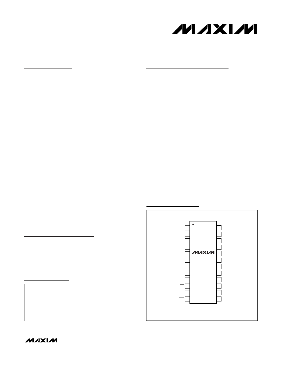
TOP VIEW
1
HBEN
2
D7
3
D6
4
D5
5
D4
D3
D2
D1/D9
D0/D8
INT
RD
MAX1064
6
7
8
9
10
11
12
QSOP
24
23
22
21
20
19
18
17
16
15
14
13
V
LOGIC
V
DD
REF
REFADJ
GND
COM
CH0
CH1
CH2
CH3
CS
CLKWR
Page 2
MAX1060/MAX1064
400ksps, +5V, 8-/4-Channel, 10-Bit ADCs
with +2.5V Reference and Parallel Interface
2 _______________________________________________________________________________________
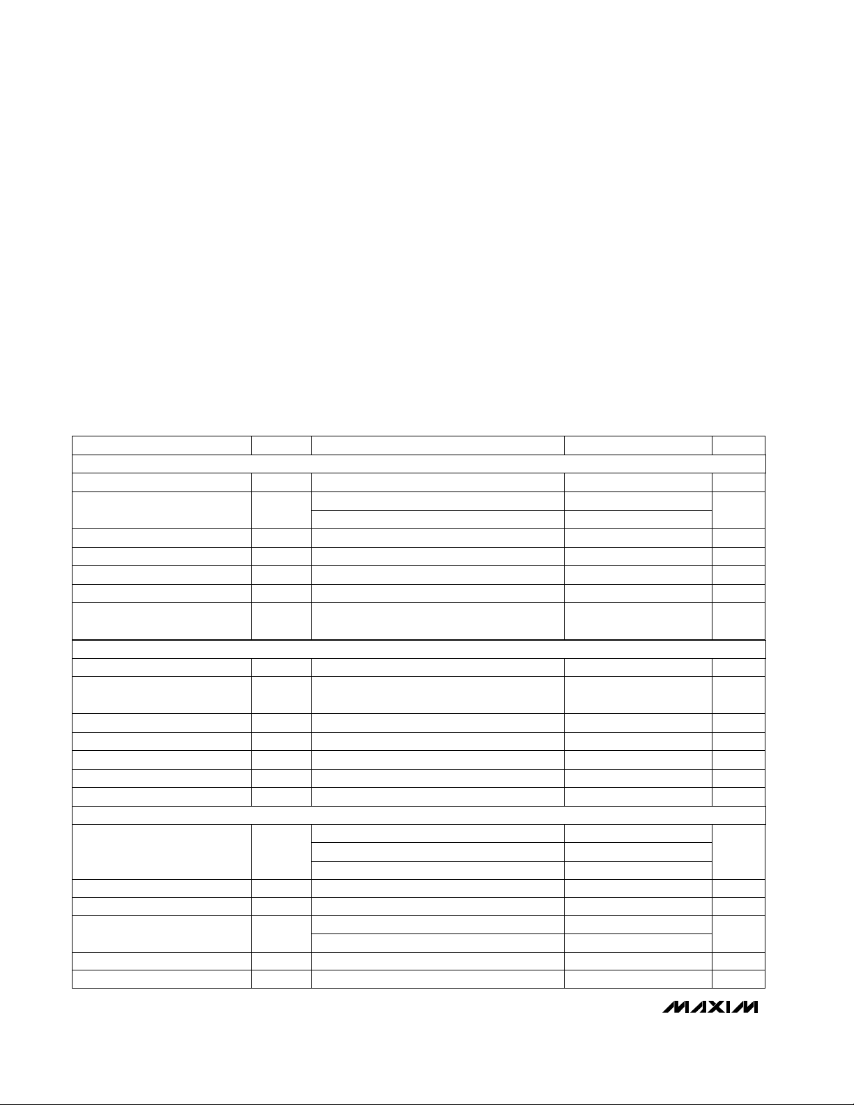
ABSOLUTE MAXIMUM RATINGS
ELECTRICAL CHARACTERISTICS
(VDD= V
LOGIC
= +5V ±10%, COM = GND, REFADJ = VDD, V
REF
= +2.5V, 4.7µF capacitor at REF pin, f
CLK
= 7.6MHz (50% duty
cycle), T
A
= T
MIN
to T
MAX
, unless otherwise noted. Typical values are at TA= +25°C.)
Stresses beyond those listed under “Absolute Maximum Ratings” may cause permanent damage to the device. These are stress ratings only, and functional
operation of the device at these or any other conditions beyond those indicated in the operational sections of the specifications is not implied. Exposure to
absolute maximum rating conditions for extended periods may affect device reliability.
External acquisition or external clock mode
Internal acquisition/internal clock mode
MAX106_A
External acquisition/internal clock mode
External clock mode
-3dB rolloff
SINAD > 56dB
fIN= 175kHz, VIN= 2.5V
P-P
(Note 4)
f
IN1
= 49kHz, f
IN2
= 52kHz
MAX106_B
No missing codes over temperature
(Note 3)
CONDITIONS
ns25Aperture Delay
ns400t
ACQ
T/H Acquisition Time
µs
3.2 3.6 4
2.5 3.0 3.5
2.1
t
CONV
Conversion Time (Note 5)
MHz
6
Full-Power Bandwidth
kHz
350
Full-Linear Bandwidth
dB
-78
Channel-to-Channel Crosstalk
dB
76
IMDIntermodulation Distortion
dB72SFDRSpurious-Free Dynamic Range
dB-72
Total Harmonic Distortion
(Including 5th-Order Harmonic)
THD
±0.5
INLRelative Accuracy (Note 2)
Bits
10
RESResolution
dB60SINADSignal-to-Noise Plus Distortion
LSB
±0.1
Channel-to-Channel Offset
Matching
ppm/°C
±2.0
Gain Temperature Coefficient
LSB
±1
LSB
±1
DNLDifferential Nonlinearity
LSB
±2
Offset Error
LSB
±2
Gain Error
UNITSMIN TYP MAXSYMBOLPARAMETER
Internal acquisition/internal clock mode
External acquisition or external clock mode
<200
ps
<50
Aperture Jitter
MHz0.1 7.6f
CLK
External Clock Frequency
%30 70Duty Cycle
DC ACCURACY (Note 1)
DYNAMIC SPECIFICATIONS (f
IN
(sine wave)
= 50kHz, VIN= 2.5V
P-P
, 400ksps, external f
CLK
= 7.6MHz, bipolar input mode)
CONVERSION RATE
VDDto GND..............................................................-0.3V to +6V
V
LOGIC
to GND.........................................................-0.3V to +6V
CH0–CH7, COM to GND............................-0.3V to (V
DD
+ 0.3V)
REF, REFADJ to GND.................................-0.3V to (V
DD
+ 0.3V)
Digital Inputs to GND ...............................................-0.3V to +6V
Digital Outputs (D0–D9, INT)
to GND ..............................................-0.3V to (V
LOGIC
+ 0.3V)
Continuous Power Dissipation (T
A
= +70°C)
24-Pin QSOP (derate 9.5mW/°C above +70°C)...........762mW
28-Pin QSOP (derate 8.0mW/°C above +70°C)...........667mW
Operating Temperature Ranges
MAX1060_C_ _/MAX1064_C_ _......................... 0°C to +70°C
MAX1060_E_ _/MAX1064_E_ _ .......................-40°C to +85°C
Storage Temperature Range .............................-65°C to +150°C
Lead Temperature (soldering, 10s) .................................+300°C
Page 3
V
MAX1060/MAX1064
400ksps, +5V, 8-/4-Channel, 10-Bit ADCs
with +2.5V Reference and Parallel Interface
_______________________________________________________________________________________ 3
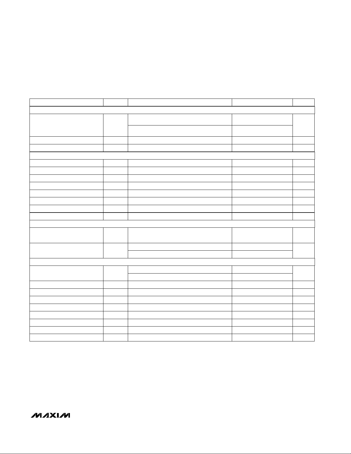
ELECTRICAL CHARACTERISTICS (continued)
(VDD= V
LOGIC
= +5V ±10%, COM = GND, REFADJ = VDD, V
REF
= +2.5V, 4.7µF capacitor at REF pin, f
CLK
= 7.6MHz (50% duty
cycle), T
A
= T
MIN
to T
MAX
, unless otherwise noted. Typical values are at TA= +25°C.)
CONDITIONS UNITSMIN TYP MAXSYMBOLPARAMETER
0 to 0.5mA output load (Note 7)
To power down the internal reference
For small adjustments
On-/off-leakage current, VIN= 0 or V
DD
Unipolar, V
COM
= 0
V
1.0
V
DD
+
50mV
V
REF
REF Input Voltage Range
µF
4.7 10
Capacitive Bypass at REF
µF
0.01 1
Capacitive Bypass at REFADJ
mV/mA
0.2
Load Regulation
V
VDD- 1.0
REFADJ High Threshold
mV
±100
REFADJ Input Range
±20 ppm/°CTC
REF
REF Temperature Coefficient
mA
15
REF Short-Circuit Current
V
2.49 2.5 2.51
REF Output Voltage
pF
12
C
IN
Input Capacitance
µA
±0.01 ±1
Multiplexer Leakage Current
V
Analog Input Voltage Range,
Single Ended and Differential
(Note 6)
0V
REF
V
IN
CS = V
DD
I
SOURCE
= 1mA
I
SINK
= 1.6mA
VIN= 0 or V
DD
V
LOGIC
= 4.5V or 2.7V
V
LOGIC
= 4.5V
µA
±0.1 ±1
I
LEAKAGE
Tri-State Leakage Current
V
V
LOGIC
- 0.5
V
OH
Output Voltage High
V
0.4
V
OL
Output Voltage Low
pF
15
C
IN
Input Capacitance
µA
±0.1 ±1
I
IN
Input Leakage Current
mV
200
V
HYS
Input Hysteresis
V
0.8
V
IL
Input Voltage Low
V
4.0
CS = V
DD
pF
15
C
OUT
Tri-State Output Capacitance
Bipolar, V
COM
= V
REF
/ 2
-V
REF
/ 2 +V
REF
/ 2
V
LOGIC
= 2.7V
2.0
V
IH
Input Voltage High
TA= 0°C to +70°C
V
REF
= 2.5V, f
SAMPLE
= 400ksps
200 300
Shutdown mode
µA
2
I
REF
Shutdown REF Input Current
ANALOG INPUTS
INTERNAL REFERENCE
EXTERNAL REFERENCE AT REF
DIGITAL INPUTS AND OUTPUTS
Page 4
Operating mode,
MAX1060/MAX1064
400ksps, +5V, 8-/4-Channel, 10-Bit ADCs
with +2.5V Reference and Parallel Interface
4 _______________________________________________________________________________________
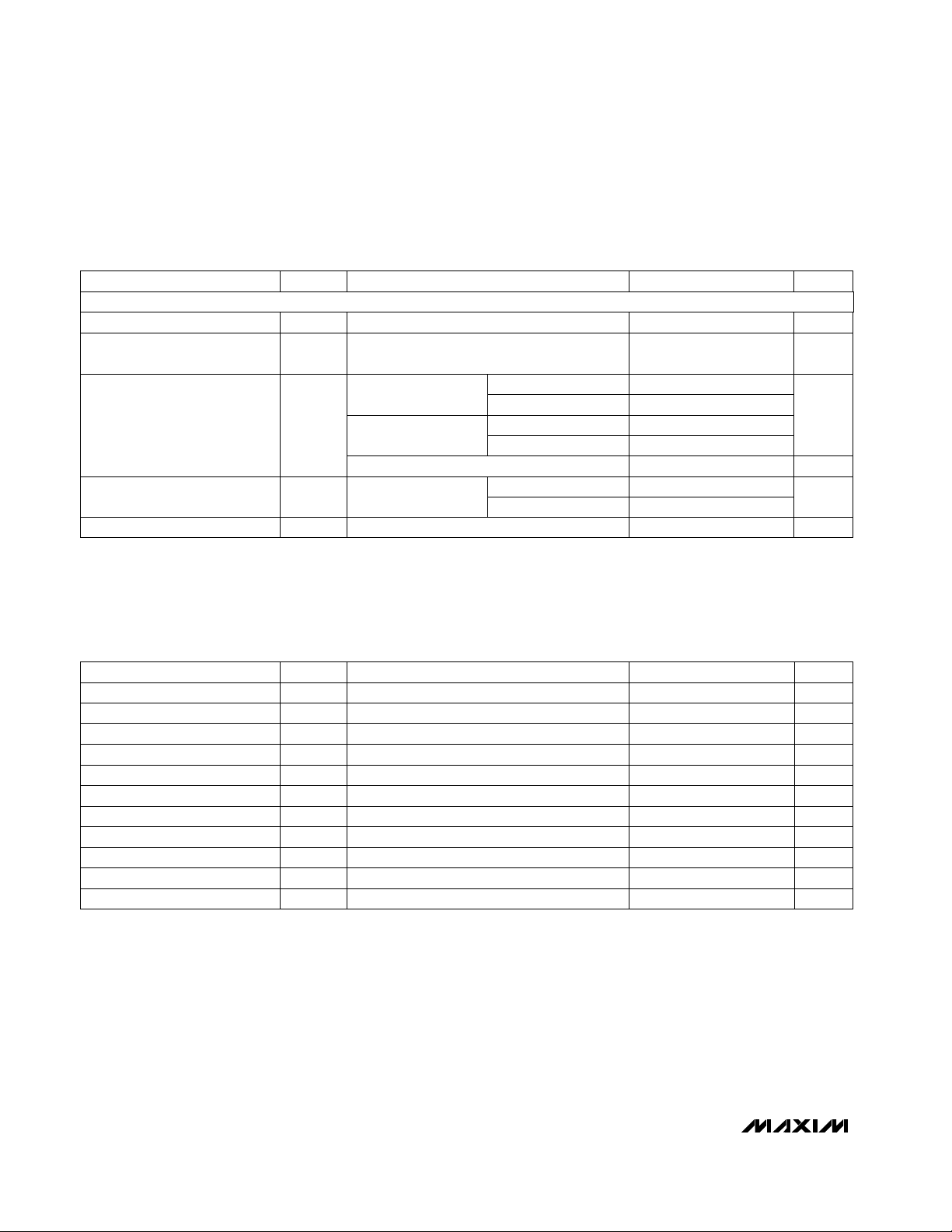
TIMING CHARACTERISTICS
(VDD= V
LOGIC
= +5V ±10%, COM = GND, REFADJ = VDD, V
REF
= +2.5V, 4.7µF capacitor at REF pin, f
CLK
= 7.6MHz (50% duty
cycle), T
A
= T
MIN
to T
MAX
, unless otherwise noted. Typical values are at TA= +25°C.)
CONDITIONS UNITSMIN TYP MAXSYMBOLPARAMETER
Standby mode
Operating mode,
f
SAMPLE
= 400ksps
1.0 1.2
mA
2.5 2.9
2.9 3.4
I
DD
Positive Supply Current
V
4.5 5.5
V
DD
Analog Supply Voltage
200
ELECTRICAL CHARACTERISTICS (continued)
(VDD= V
LOGIC
= +5V ±10%, COM = GND, REFADJ = VDD, V
REF
= +2.5V, 4.7µF capacitor at REF pin, f
CLK
= 7.6MHz (50% duty
cycle), T
A
= T
MIN
to T
MAX
, unless otherwise noted. Typical values are at TA= +25°C.)
V
LOGIC
Current I
LOGIC
CL= 20pF
210
µA
Power-Supply Rejection PSR VDD= 5V ±10%, full-scale input
±0.3 ±0.9
mV
f
SAMPLE
= 400ksps
Nonconverting
V
2.7
V
DD
+
0.3
V
LOGIC
Digital Supply Voltage
WR to CLK Fall Setup Time
t
CWS
40
ns
nsCLK Pulse Width High
nsCLK Period
t
CH
40
t
CP
132
CLK Pulse Width Low t
CL
40
ns
Data Valid to WR Rise Time
t
DS
40
ns
WR Rise to Data Valid Hold Time
t
DH
0
ns
CLK Fall to WR Hold Time
t
CWH
40
ns
CS to CLK or WR Setup Time
t
CSWS
60
ns
CLK or WR to CS Hold Time
t
CSWH
0
ns
CS Pulse Width
t
CS
100
ns
WR Pulse Width
t
WR
60
ns(Note 8)
PARAMETER SYMBOL MIN TYP MAX UNITSCONDITIONS
Shutdown mode
210
0.5 0.8
POWER REQUIREMENTS
µA
External reference
Internal reference
External reference
Internal reference
Page 5
MAX1060/MAX1064
400ksps, +5V, 8-/4-Channel, 10-Bit ADCs
with +2.5V Reference and Parallel Interface
_______________________________________________________________________________________ 5
Note 1: Tested at VDD= +5V, COM = GND, unipolar single-ended input mode.
Note 2: Relative accuracy is the deviation of the analog value at any code from its theoretical value after offset and gain errors have
been removed.
Note 3: Offset nulled.
Note 4: On channel is grounded; sine wave applied to off channels.
Note 5: Conversion time is defined as the number of clock cycles times the clock period; clock has 50% duty cycle.
Note 6: Input voltage range referenced to negative input. The absolute range for the analog inputs is from GND to V
DD
.
Note 7: External load should not change during conversion for specified accuracy.
Note 8: When bit 5 is set low for internal acquisition, WR must not return low until after the first falling clock edge of the conversion.
TIMING CHARACTERISTICS (continued)
(VDD= V
LOGIC
= +5V ±10%, COM = GND, REFADJ = VDD, V
REF
= +2.5V, 4.7µF capacitor at REF pin, f
CLK
= 7.6MHz (50% duty
cycle), T
A
= T
MIN
to T
MAX
, unless otherwise noted. Typical values are at TA= +25°C.)
Figure 1. Load Circuits for Enable/Disable Times
t
TR
10 40
nsC
LOAD
= 20pF, Figure 1
RD Rise to Output Disable
RD Fall to Output Data Valid
t
DO
10 50
ns
RD Fall to INT High Delay
t
INT1
50
ns
CS Fall to Output Data Valid
t
DO2
100
ns
C
LOAD
= 20pF, Figure 1
C
LOAD
= 20pF, Figure 1
C
LOAD
= 20pF, Figure 1
t
TC
10 60
nsC
LOAD
= 20pF, Figure 1
PARAMETER SYMBOL MIN TYP MAX UNITSCONDITIONS
CS Rise to Output Disable
HBEN Rise to Output Data Valid t
DO1
10 50
nsC
LOAD
= 20pF, Figure 1
HBEN Fall to Output Data Valid t
DO1
10 80
nsC
LOAD
= 20pF, Figure 1
V
LOGIC
3kΩ
DOUT
3kΩ
a) HIGH-Z TO VOH AND VOL TO V
C
LOAD
20pF
OH
DOUT
b) HIGH-Z TO VOL AND VOH TO V
C
LOAD
20pF
OL
Page 6
MAX1060/MAX1064
400ksps, +5V, 8-/4-Channel, 10-Bit ADCs
with +2.5V Reference and Parallel Interface
6 _______________________________________________________________________________________
Typical Operating Characteristics
(VDD= V
LOGIC
= +5V, V
REF
= +2.500V, f
CLK
= 7.6MHz, CL= 20pF, TA= +25°C, unless otherwise noted.)
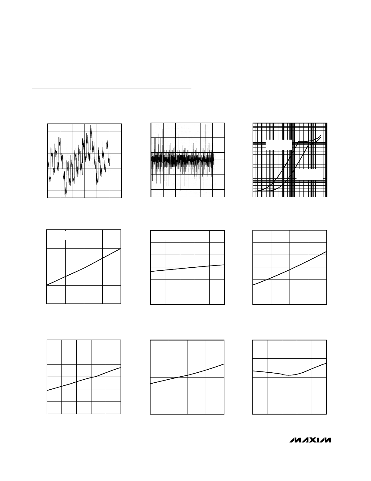
-0.25
-0.10
-0.15
-0.20
-0.05
0
0.05
0.10
0.15
0.20
0.25
0 400200 600 800 1000 1200
INTEGRAL NONLINEARITY
vs. OUTPUT CODE
MAX1060/64 toc01
OUTPUT CODE
INL (LSB)
0.1 10k101 100 1k 100k 1M
SUPPLY CURRENT
vs. SAMPLE FREQUENCY
MAX1060/64 toc03
f
SAMPLE
(Hz)
I
DD
(µA)
1
10
100
1k
10k
WITH INTERNAL
REFERENCE
WITH EXTERNAL
REFERENCE
1.8
1.9
2.0
2.1
2.2
SUPPLY CURRENT vs. SUPPLY VOLTAGE
MAX1060/64 toc04
VDD (V)
I
DD
(mA)
4.50 5.004.75 5.25 5.50
RL = ∞
CODE = 1010100000
1.7
1.9
1.8
2.1
2.0
2.2
2.3
-40 10-15 35 60 85
SUPPLY CURRENT vs. TEMPERATURE
MAX1060/64 toc05
TEMPERATURE (°C)
I
DD
(mA)
RL = ∞
CODE = 1010100000
930
950
940
970
960
980
990
4.50 5.004.75 5.25 5.50
STANDBY CURRENT vs. SUPPLY VOLTAGE
MAX1060/64 toc06
VDD (V)
STANDBY I
DD
(µA)
930
950
940
970
960
980
990
-40 10-15 35 60 85
STANDBY CURRENT vs. TEMPERATURE
MAX1060/64 toc07
TEMPERATURE (°C)
STANDBY I
DD
(µA)
1.0
1.5
2.0
2.5
3.0
POWER-DOWN CURRENT
vs. SUPPLY VOLTAGE
MAX1060/64 toc08
VDD (V)
POWER-DOWN I
DD
(µA)
4.50 5.004.75 5.25 5.50
1.8
2.0
1.9
2.1
2.2
-40 10-15 35 60 85
POWER-DOWN CURRENT
vs. TEMPERATURE
MAX1060/64 toc09
TEMPERATURE (°C)
POWER-DOWN I
DD
(µA)
-0.25
-0.10
-0.15
-0.20
-0.05
0
0.05
0.10
0.15
0.20
0.25
0 400200 600 800 1000 1200
DIFFERENTIAL NONLINEARITY
vs. OUTPUT CODE
MAX1060/64 toc02
OUTPUT CODE
DNL (LSB)
Page 7

MAX1060/MAX1064
400ksps, +5V, 8-/4-Channel, 10-Bit ADCs
with +2.5V Reference and Parallel Interface
_______________________________________________________________________________________ 7
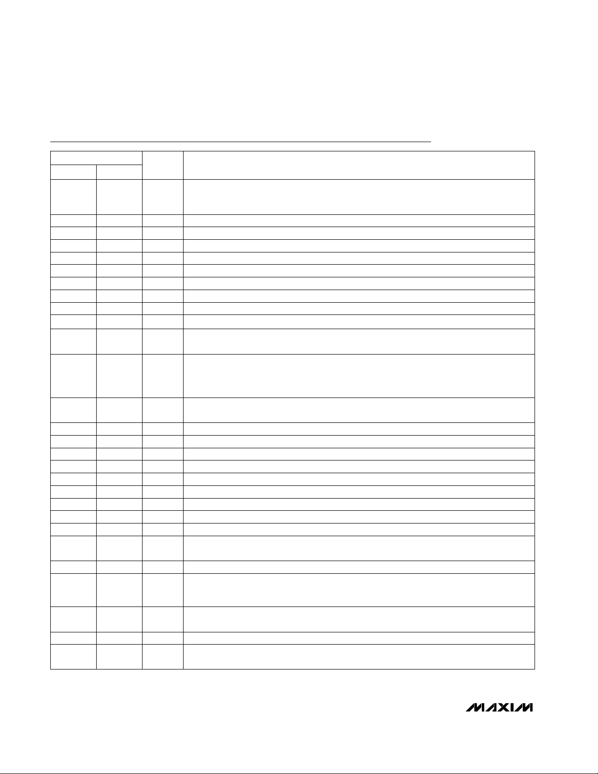
Typical Operating Characteristics (continued)
(VDD= V
LOGIC
= +5V, V
REF
= +2.500V, f
CLK
= 7.6MHz, CL= 20pF, TA= +25°C, unless otherwise noted.)
0
50
150
100
200
250
-40 10-15 35 60 85
LOGIC SUPPLY CURRENT
vs. TEMPERATURE
MAX1060/64 toc17
TEMPERATURE (°C)
I
LOGIC
(µA)
-140
-120
-100
-80
-60
-40
-20
0
20
0 400200 600 800 1000 1200
FFT PLOT
MAX1060/64 toc18
FREQUENCY (kHz)
AMPLITUDE (dB)
VDD = 5V
f
IN
= 50kHz
f
SAMPLE
= 400ksps
INTERNAL REFERENCE VOLTAGE
vs. SUPPLY VOLTAGE
2.53
2.52
2.51
(V)
REF
V
2.50
2.49
2.48
4.50 5.004.75 5.25 5.50
VDD (V)
OFFSET ERROR
vs. TEMPERATURE
1.0
0.5
MAX1060/64 toc10
MAX1060/64 toc13
INTERNAL REFERENCE VOLTAGE
vs. TEMPERATURE
2.53
2.52
2.51
(V)
REF
V
2.50
2.49
2.48
-40 10-15 35 60 85
TEMPERATURE (°C)
GAIN ERROR vs. SUPPLY VOLTAGE
0.50
0.25
MAX1060/64 toc11
MAX1060/64 toc14
1.0
0.5
0
OFFSET ERROR (LSB)
-0.5
-1.0
4.50 5.004.75 5.25 5.50
0.500
0.375
OFFSET ERROR
vs. SUPPLY VOLTAGE
V
DD
GAIN ERROR vs. TEMPERATURE
MAX1060/64 toc12
(V)
MAX1060/64 toc15
0
OFFSET ERROR (LSB)
-0.5
-1.0
-40 10-15 35 60 85
LOGIC SUPPLY CURRENT
vs. SUPPLY VOLTAGE
250
200
(µA)
150
LOGIC
I
100
50
4.50 5.004.75 5.25 5.50
TEMPERATURE (°C)
VDD (V)
MAX1060/64 toc16
0
GAIN ERROR (LSB)
-0.25
-0.50
4.50 5.004.75 5.25 5.50
VDD (V)
0.250
GAIN ERROR (LSB)
0.125
0
-40 35 60-15 10 85
TEMPERATURE (°C)
Page 8
MAX1060/MAX1064
400ksps, +5V, 8-/4-Channel, 10-Bit ADCs
with +2.5V Reference and Parallel Interface
8 _______________________________________________________________________________________
Pin Description
NAME FUNCTION
1 HBEN
High Byte Enable. Used to multiplex the 10-bit conversion result.
1: 2 MSBs are multiplexed on the data bus.
0: 8 LSBs are available on the data bus.
PIN
2 D7 Tri-State Digital I/O Line (D7)
3 D6 Tri-State Digital I/O Line (D6)
4 D5 Tri-State Digital I/O Line (D5)
5 D4 Tri-State Digital I/O Line (D4)
6 D3 Tri-State Digital I/O Line (D3)
7 D2 Tri-State Digital I/O Line (D2)
8 D1/D9 Tri-State Digital I/O Line (D1, HBEN = 0; D9, HBEN = 1)
9 D0/D8 Tri-State Digital I/O Line (D0, HBEN = 0; D8, HBEN = 1)
10
INT INT goes low when the conversion is complete and the output data is ready.
11
RD
Active-Low Read Select. If CS is low, a falling edge on RD enables the read operation on the
data bus.
12
WR
Active-Low Write Select. When CS is low in internal acquisition mode, a rising edge on WR
latches in configuration data and starts an acquisition plus a conversion cycle. When CS is
low in external acquisition mode, the first rising edge on WR ends acquisition and starts a
conversion.
13 CLK
Clock Input. In external clock mode, drive CLK with a TTL-/CMOS-compatible clock. In internal clock mode, connect this pin to either V
DD
or GND.
14
CS Active-Low Chip Select. When CS is high, digital outputs (D7–D0) are high impedance.
15 CH7 Analog Input Channel 7
16 CH6 Analog Input Channel 6
17 CH5 Analog Input Channel 5
18 CH4 Analog Input Channel 4
19 CH3 Analog Input Channel 3
20 CH2 Analog Input Channel 2
21 CH1 Analog Input Channel 1
22 CH0 Analog Input Channel 0
23 COM
Ground Reference for Analog Inputs. Sets zero-code voltage in single-ended mode and
must be stable to ±0.5 LSB during conversion.
24 GND Analog and Digital Ground
25 REFADJ
Bandgap Reference Output/Bandgap Reference Buffer Input. Bypass to GND with a 0.01µF
capacitor. When using an external reference, connect REFADJ to V
DD
to disable the internal
bandgap reference.
26 REF
Bandgap Reference Buffer Output/External Reference Input. Add a 4.7µF capacitor to GND
when using the internal reference.
27 V
DD
Analog +5V Power Supply. Bypass with a 0.1µF capacitor to GND.
28 V
LOGIC
Digital Power Supply. V
LOGIC
powers the digital outputs of the data converter and can range
from +2.7V to (V
DD
+ 300mV).
1
2
3
4
5
6
7
8
9
10
11
12
13
14
—
—
—
—
15
16
17
18
19
20
21
22
23
24
MAX1060 MAX1064
Page 9

MAX1060/MAX1064
400ksps, +5V, 8-/4-Channel, 10-Bit ADCs
with +2.5V Reference and Parallel Interface
_______________________________________________________________________________________ 9
Detailed Description
Converter Operation
The MAX1060/MAX1064 ADCs use a successiveapproximation (SAR) conversion technique and an
input track-and-hold (T/H) stage to convert an analog
input signal to a 10-bit digital output. Their parallel (8 + 2)
output format provides an easy interface to standard
microprocessors (µPs). Figure 2 shows the simplified
internal architecture of the MAX1060/MAX1064.
Single-Ended and
Pseudo-Differential Operation
The sampling architecture of the ADC’s analog comparator is illustrated in the equivalent input circuits in
Figures 3a and 3b. In single-ended mode, IN+ is internally switched to channels CH0–CH7 for the MAX1060
(Figure 3a) and to CH0–CH3 for the MAX1064 (Figure
3b), while IN- is switched to COM (Table 3). In differential mode, IN+ and IN- are selected from analog input
pairs (Table 4).
In differential mode, IN- and IN+ are internally switched to
either of the analog inputs. This configuration is pseudodifferential in that only the signal at IN+ is sampled. The
return side (IN-) must remain stable within ±0.5 LSB
(±0.1 LSB for best performance) with respect to GND
during a conversion. To accomplish this, connect a
0.1µF capacitor from IN- (the selected input) to GND.
During the acquisition interval, the channel selected as
the positive input (IN+) charges capacitor C
HOLD
. At
the end of the acquisition interval, the T/H switch
opens, retaining the charge on C
HOLD
as a sample of
the signal at IN+.
The conversion interval begins with the input multiplexer switching C
HOLD
from the positive input (IN+) to the
negative input (IN-). This unbalances node zero at the
comparator’s positive input. The capacitive digital-toanalog converter (DAC) adjusts during the remainder of
the conversion cycle to restore node zero to 0V within
the limits of 10-bit resolution. This action is equivalent to
transferring a 12pF [(V
IN+
) - (V
IN-
)] charge from C
HOLD
to the binary-weighted capacitive DAC, which in turn
forms a digital representation of the analog input signal.
Figure 2. Simplified Functional Diagram of 8-/4-Channel MAX1060/MAX1064
(CH7)
(CH6)
(CH5)
(CH4)
CH3
CH2
CH1
CH0
COM
CLK
WR
INT
CS
RD
( ) ARE FOR MAX1060 ONLY.
MULTIPLEXER
CLOCK
ANALOG
INPUT
CONTROL LOGIC
AND
LATCHES
REF REFADJ
T/H
CHARGE REDISTRIBUTION
10-BIT DAC
10
SUCCESSIVE-
APPROXIMATION
REGISTER
2
2
MUX
8
TRI-STATE, BIDIRECTIONAL
I/O INTERFACE
8
D0–D7
8-BIT DATA BUS
AV =
2.05
8
8
17kΩ
COMP
MAX1060
MAX1064
1.22V
REFERENCE
HBEN
V
DD
V
LOGIC
GND
Page 10

Analog Input Protection
Internal protection diodes, which clamp the analog
input to VDDand GND, allow each input channel to
swing within (GND - 300mV) to (VDD+ 300mV) without
damage. However, for accurate conversions near full
scale, neither input should exceed (VDD+ 50mV) or be
less than (GND - 50mV).
If an off-channel analog input voltage exceeds the supplies by more than 50mV, limit the forward-bias input
current to 4mA.
Track/Hold
The MAX1060/MAX1064 T/H stage enters its tracking
mode on the rising edge of WR. In external acquisition
mode, the part enters its hold mode on the next rising
edge of WR. In internal acquisition mode, the part enters
its hold mode on the fourth falling edge of the clock after
writing the control byte. Note that, in internal clock mode,
this is approximately 1µs after writing the control byte.
In single-ended operation, IN- is connected to COM
and the converter samples the positive (+) input. In
pseudo-differential operation, IN- connects to the negative input (-) and the difference of |(IN+) - (IN-)|is sampled. At the beginning of the next conversion, the
positive input connects back to IN+ and C
HOLD
charges to the input signal.
The time required for the T/H stage to acquire an input
signal depends on how quickly its input capacitance is
charged. If the input signal’s source impedance is high,
the acquisition time lengthens and more time must be
allowed between conversions. The acquisition time,
t
ACQ
, is the maximum time the device takes to acquire
the signal and is also the minimum time required for the
signal to be acquired. Calculate this with the following
equation:
t
ACQ
= 7(RS + RIN)C
IN
where RSis the source impedance of the input signal,
RIN(800Ω) is the input resistance, and CIN(12pF) is
the input capacitance of the ADC. Source impedances
below 3kΩ have no significant impact on the MAX1060/
MAX1064s’ AC performance.
Higher source impedances can be used if a 0.01µF
capacitor is connected to the individual analog inputs.
Along with the input impedance, this capacitor forms
an RC filter, limiting the ADC’s signal bandwidth.
Input Bandwidth
The MAX1060/MAX1064 T/H stage offers a 350kHz fulllinear and a 6MHz full-power bandwidth. These features make it possible to digitize high-speed transients
and measure periodic signals with bandwidths exceeding the ADC’s sampling rate by using undersampling
techniques. To avoid aliasing high-frequency signals
into the frequency band of interest, anti-alias filtering is
recommended.
Starting a Conversion
Initiate a conversion by writing a control byte that
selects the multiplexer channel and configures the
MAX1060/MAX1064 for either unipolar or bipolar operation. A write pulse (WR + CS) can either start an acquisition interval or initiate a combined acquisition plus
conversion. The sampling interval occurs at the end of
MAX1060/MAX1064
400ksps, +5V, 8-/4-Channel, 10-Bit ADCs
with +2.5V Reference and Parallel Interface
10 ______________________________________________________________________________________
Figure 3a. MAX1060 Simplified Input Structure
Figure 3b. MAX1064 Simplified Input Structure
10-BIT CAPACITIVE DAC
REF
INPUT
C
–
C
SWITCH
HOLD
12pF
TRACK
SWITCH
ZERO
+
R
IN
800Ω
HOLD
T/H
CH0
CH1
CH2
CH3
CH4
CH5
CH6
CH7
COM
SINGLE-ENDED MODE: IN+ = CH0–CH7, IN- = COM
PSEUDO-DIFFERENTIAL MODE: IN+ AND IN- SELECTED FROM PAIRS CH0/CH1,
CH2/CH3, CH4/CH5, AND CH6/CH7
MUX
COMPARATOR
AT THE SAMPLING INSTANT,
THE MUX INPUT SWITCHES
FROM THE SELECTED IN+
CHANNEL TO THE SELECTED
IN- CHANNEL.
10-BIT CAPACITIVE DAC
REF
INPUT
C
–
C
SWITCH
HOLD
12pF
TRACK
+
T/H
SWITCH
R
IN
800Ω
ZERO
HOLD
CH0
CH1
CH2
CH3
COM
SINGLE-ENDED MODE: IN+ = CH0–CH3, IN- = COM
PSEUDO-DIFFERENTIAL MODE: IN+ AND IN- SELECTED FROM PAIRS CH0/CH1
AND CH2/CH3
MUX
COMPARATOR
AT THE SAMPLING INSTANT,
THE MUX INPUT SWITCHES
FROM THE SELECTED IN+
CHANNEL TO THE SELECTED
IN- CHANNEL.
Page 11

MAX1060/MAX1064
400ksps, +5V, 8-/4-Channel, 10-Bit ADCs
with +2.5V Reference and Parallel Interface
______________________________________________________________________________________ 11
Table 1. Control Byte Functional Description
NAME FUNCTION
D4
0
SGL/DIF
SGL/DIF = 0: Pseudo-differential analog input mode
SGL/DIF = 1: Single-ended analog input mode
In single-ended mode, input signals are referred to COM. In pseudo-differential mode, the voltage
difference between two channels is measured (Tables 2 and 3).
10
D3
UNI/BIP
Standby power-down mode. Clock mode is unaffected.
0
11
UNI/BIP = 0: Bipolar mode
UNI/BIP = 1: Unipolar mode
In unipolar mode, an analog input signal from 0 to V
REF
can be converted; in bipolar mode, the
signal can range from -V
REF
/2 to +V
REF
/2.
D2, D1, D0
Normal operation mode. External clock mode is selected.
1
A2, A1, A0
Address bits A2, A1, A0 select which of the 8/4 (MAX1060/MAX1064) channels are to be converted
(Tables 3 and 4).
Normal operation mode. Internal clock mode is selected.
BIT
PD1, PD0
0
D7, D6
PD1 and PD0 select the various clock and power-down modes.
Full power-down mode. Clock mode is unaffected.
D5 ACQMOD
ACQMOD = 0: Internal acquisition mode
ACQMOD = 1: External acquisition mode
the acquisition interval. The ACQMOD (acquisition
mode) bit in the input control byte (Table 1) offers two
options for acquiring the signal: an internal and an
external acquisition. The conversion period lasts for 13
clock cycles in either the internal or external clock or
acquisition mode. Writing a new control byte during a
conversion cycle aborts the conversion and starts a
new acquisition interval.
Internal Acquisition
Select internal acquisition by writing the control byte
with the ACQMOD bit cleared (ACQMOD = 0). This
causes the write pulse to initiate an acquisition interval
whose duration is internally timed. Conversion starts
when this acquisition interval (three external clock
cycles or approximately 1µs in internal clock mode)
ends (Figure 4). When the internal acquisition is combined with the internal clock, the aperture jitter can be
as high as 200ps. Internal clock users wishing to
achieve the 50ps jitter specification should always use
external acquisition mode.
External Acquisition
Use external acquisition mode for precise control of the
sampling aperture and/or dependent control of acquisition and conversion times. The user controls acquisition
and start-of-conversion with two separate write pulses.
The first pulse, written with ACQMOD = 1, starts an
acquisition interval of indeterminate length. The second
write pulse, written with ACQMOD = 0 (all other bits in
the control byte are unchanged), terminates acquisition
and starts conversion on WR rising edge (Figure 5).
The address bits for the input multiplexer must have the
same values on the first and second write pulses.
Power-down mode bits (PD0, PD1) can assume new
values on the second write pulse (see the Power-Down
Modes section). Changing other bits in the control byte
corrupts the conversion.
Reading a Conversion
A standard interrupt signal, INT, is provided to allow the
MAX1060/MAX1064 to flag the µP when the conversion
has ended and a valid result is available. INT goes low
when the conversion is complete and the output data is
ready (Figures 4 and 5). INT returns high on the first
read cycle or if a new control byte is written.
Selecting Clock Mode
The MAX1060/MAX1064 operate with an internal or
external clock. Control bits D6 and D7 select either
internal or external clock mode. The part retains the
last-requested clock mode if a power-down mode is
selected in the current input word. For both internal and
external clock modes, internal or external acquisition
can be used. At power-up, the MAX1060/MAX1064
enter the default external clock mode.
Page 12

MAX1060/MAX1064
400ksps, +5V, 8-/4-Channel, 10-Bit ADCs
with +2.5V Reference and Parallel Interface
12 ______________________________________________________________________________________
Figure 4. Conversion Timing Using Internal Acquisition Mode
Figure 5. Conversion Timing Using External Acquisition Mode
t
CS
CS
WR
D7–D0
INT
RD
HBEN
t
CSWS
t
WR
t
DS
CONTROL
BYTE
ACQMOD = 0
t
ACQ
t
t
DH
CSWH
DOUT
CS
t
CSWS
WR
D7–D0
t
DS
t
CS
t
WR
CONTROL
BYTE
ACQMOD = 1
t
CSHW
t
DH
t
ACQ
t
CONV
CONTROL
BYTE
ACQMOD = 0
t
CONV
t
INT1
t
D0
HIGH/LOW
BYTE VALID
t
D01
HIGH/LOW
BYTE VALID
t
INT1
t
TR
HIGH-ZHIGH-Z
INT
RD
HBEN
t
t
D0
HIGH-Z HIGH-Z
DOUT
D01
HIGH/LOW
BYTE VALID
HIGH/LOW
BYTE VALID
t
TR
Page 13

Internal Clock Mode
Select internal clock mode to release the µP from the
burden of running the SAR conversion clock. To select
this mode, bit D7 of the control byte must be set to 1 and
bit D6 must be set to zero. The internal clock frequency
is then selected, resulting in a 3.6µs conversion time.
When using the internal clock mode, connect the CLK
pin either high or low to prevent the pin from floating.
External Clock Mode
To select the external clock mode, bits D6 and D7 of
the control byte must be set to 1. Figure 6 shows the
clock and WR timing relationship for internal (Figure 6a)
and external (Figure 6b) acquisition modes with an
external clock. Proper operation requires a 100kHz to
7.6MHz clock frequency with 30% to 70% duty cycle.
Operating the MAX1060/MAX1064 with clock frequencies lower than 100kHz is not recommended, because
it causes a voltage droop across the hold capacitor in
the T/H stage that results in degraded performance.
MAX1060/MAX1064
400ksps, +5V, 8-/4-Channel, 10-Bit ADCs
with +2.5V Reference and Parallel Interface
______________________________________________________________________________________ 13
Figure 6a. External Clock and WRTiming (Internal Acquisition Mode)
Figure 6b. External Clock and WRTiming (External Acquisition Mode)
CLK
WR
CLK
WR
t
CWH
ACQMOD = 0
ACQMOD = 0
ACQUISITION STARTS
ACQUISITION STARTS
t
CWS
t
CP
t
CH
ACQUISITION ENDS
t
CL
WR GOES HIGH WHEN CLK IS HIGH.
ACQUISITION ENDS
WR GOES HIGH WHEN CLK IS LOW.
CONVERSION STARTS
CONVERSION STARTS
ACQUISITION STARTS
CLK
t
DH
WR
WR GOES HIGH WHEN CLK IS HIGH.
WR GOES HIGH WHEN CLK IS LOW.
CLK
WR
ACQMOD = 1
ACQMOD = 1
ACQUISITION STARTS
t
DH
ACQUISITION ENDS
ACQUISITION ENDS
t
CWH
ACQMOD = "0"
t
CWS
ACQMOD = "0"
CONVERSION STARTS
CONVERSION STARTS
Page 14

MAX1060/MAX1064
Digital Interface
Input (control byte) and output data are multiplexed on a
tri-state parallel interface. This parallel interface (I/O) can
easily be interfaced with standard µPs. Signals CS, WR,
and RD control the write and read operations. CS represents the chip-select signal, which enables a µP to
address the MAX1060/MAX1064 as an I/O port. When
high, CS disables the CLK, WR, and RD inputs and
forces the interface into a high-impedance (high-Z) state.
Input Format
The control byte is latched into the device on pins D7–
D0 during a write command. Table 2 shows the control
byte format.
Output Format
The output format for the MAX1060/MAX1064 is binary in
unipolar mode and two’s complement in bipolar mode.
When reading the output data, CS and RD must be low.
When HBEN = 0, the lower 8 bits are read. With HBEN =
1, the upper 2 bits are available and the output data bits
D7–D2 are set either low in unipolar mode or to the value
of the MSB in bipolar mode (Table 5).
400ksps, +5V, 8-/4-Channel, 10-Bit ADCs
with +2.5V Reference and Parallel Interface
14 ______________________________________________________________________________________
Table 2. Control Byte Format
Table 4. Channel Selection for Pseudo-Differential Operation (SGL/DIF = 0)
Table 3. Channel Selection for Single-Ended Operation (SGL/DIF = 1)
*Channels CH4–CH7 apply to MAX1060 only.
*Channels CH4
–CH7 apply to MAX1060 only.
A1 CH0
0 +0 -0
A0
0 -1
CH2 CH4*
+0
1 0 + -
CH3
0
CH1 CH7*CH6*
1
CH5*
1 - +0
0 0
A2
+ -1
0 1 - +1
1 0 -1
1 1
+
1 +-
A1 CH0
0 +00
A0
0 1
CH2 CH4*
+0
1 0 +
CH3
-
0
CH1 CH7*
-
CH6*
-
COM
1
CH5*
1 + -0
0 0
A2
+1
0 1 +1
-
-
1 01
1 1
+
1
-
+ -
D6 D4
PD0
SGL/DIF
ACQMOD A2 A0A1
UNI/BIP
PD1
D5 D2 D0 (LSB)D1D3D7 (MSB)
Page 15

___________Applications Information
Power-On Reset
When power is first applied, internal power-on reset circuitry activates the MAX1060/MAX1064 in external
clock mode and sets INT high. After the power supplies
stabilize, the internal reset time is 10µs, and no conversions should be attempted during this phase. When
using the internal reference, 500µs are required for
V
REF
to stabilize.
Internal and External Reference
The MAX1060/MAX1064 can be used with an internal
or external reference voltage. An external reference
can be connected directly to REF or REFADJ.
An internal buffer is designed to provide +2.5V at REF
for both devices. The internally trimmed +1.22V reference is buffered with a +2.05V/V gain.
Internal Reference
The full-scale range with the internal reference is +2.5V
with unipolar inputs and ±1.25V with bipolar inputs. The
internal reference buffer allows for small adjustments
(±100mV) in the reference voltage (Figure 7).
Note: The reference buffer must be compensated with
an external capacitor (4.7µF min) connected between
REF and GND to reduce reference noise and switching
spikes from the ADC. To further minimize reference
noise, connect a 0.01µF capacitor between REFADJ
and GND.
External Reference
With the MAX1060/MAX1064, an external reference can
be placed at either the input (REFADJ) or the output
(REF) of the internal reference-buffer amplifier.
Using the REFADJ input makes buffering the external
reference unnecessary. The REFADJ input impedance
is typically 17kΩ.
When applying an external reference to REF, disable
the internal reference buffer by connecting REFADJ to
V
DD
. The DC input resistance at REF is 25kΩ.
Therefore, an external reference at REF must deliver up
to 200µA DC load current during a conversion and
have an output impedance less than 10Ω. If the reference has higher output impedance or is noisy, bypass
it close to the REF pin with a 4.7µF capacitor.
Power-Down Modes
To save power, place the converter in a low-current
shutdown state between conversions. Select standby
mode or shutdown mode using bits D6 and D7 of the
control byte (Tables 1 and 2). In both software powerdown modes, the parallel interface remains active, but
the ADC does not convert.
Standby Mode
While in standby mode, the supply current is 1mA (typ).
The part powers up on the next rising edge on WR and
is ready to perform conversions. This quick turn-on time
allows the user to realize significantly reduced power
consumption for conversion rates below 400ksps.
Shutdown Mode
Shutdown mode turns off all chip functions that draw
quiescent current, reducing the typical supply current
to 2µA immediately after the current conversion is completed. A rising edge on WR causes the MAX1060/
MAX1064 to exit shutdown mode and return to normal
operation. To achieve full 10-bit accuracy with a 4.7µF
reference bypass capacitor, 500µs is required after
power-up. Waiting 500µs in standby mode, instead of in
full-power mode, can reduce power consumption by a
factor of 3 or more. When using an external reference,
MAX1060/MAX1064
400ksps, +5V, 8-/4-Channel, 10-Bit ADCs
with +2.5V Reference and Parallel Interface
______________________________________________________________________________________ 15
Table 5. Data-Bus Output (8 + 2 Parallel
Interface)
Figure 7. Reference Voltage Adjustment with External
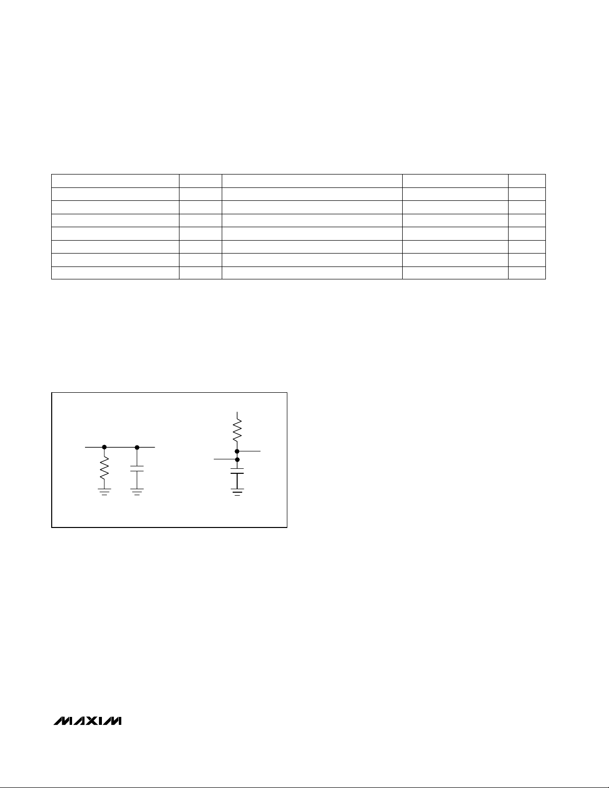
Potentiometer
PIN HBEN = 0 HBEN = 1
D0 Bit 0 (LSB) Bit 8
D1 Bit 1 Bit 9 (MSB)
BIPOLAR
(UNI/BIP = 0)
UNIPOLAR
(UNI/BIP = 1)
D2 Bit 2 Bit 9 0
D5 Bit 5 Bit 9 0
D6 Bit 6 Bit 9 0
D7 Bit 7 Bit 9 0
D4 Bit 4 Bit 9 0
D3 Bit 3 Bit 9 0
VDD = +5V
50kΩ
MAX1060
MAX1064
REFADJ
REF
GND
330kΩ
0.01µF
4.7µF
50kΩ
Page 16

MAX1060/MAX1064
only 50µs are required after power-up. Enter standby
mode by performing a dummy conversion with the control byte specifying standby mode.
Note: Bypass capacitors larger than 4.7µF between
REF and GND result in longer power-up delays.
Transfer Function
Table 6 shows the full-scale voltage ranges for unipolar
and bipolar modes.
Figure 8 depicts the nominal, unipolar input/output (I/O)
transfer function, and Figure 9 shows the bipolar I/O
transfer function. Code transitions occur halfway
between successive-integer LSB values. Output coding
is binary, with 1 LSB = V
REF
/ 1024.
Maximum Sampling Rate/
Achieving 475ksps
When running at the maximum clock frequency of
7.6MHz, the specified 400ksps throughput is achieved
by completing a conversion every 19 clock cycles: 1
write cycle, 3 acquisition cycles, 13 conversion cycles,
and 2 read cycles. This assumes that the results of the
last conversion are read before the next control byte is
written. It is possible to achieve higher throughputs
(Figure 10), up to 475ksps, by first writing a control
word to begin the acquisition cycle of the next conversion, then reading the results of the previous conversion from the bus. This technique allows a conversion
to be completed every 16 clock cycles. Note that
switching the data bus during acquisition or conversion
can cause additional supply noise that can make it difficult to achieve true 10-bit performance.
Layout, Grounding, and Bypassing
For best performance, use printed circuit boards. Wirewrap configurations are not recommended since the layout should ensure proper separation of analog and digital
traces. Do not run analog and digital lines parallel to each
other, and do not lay out digital signal paths underneath
the ADC package. Use separate analog and digital PC
board ground sections with only one star point (Figure
11) connecting the two ground systems (analog and digital). For lowest noise operation, ensure the ground return
to the star ground’s power supply is low impedance and
as short as possible. Route digital signals far away from
sensitive analog and reference inputs.
400ksps, +5V, 8-/4-Channel, 10-Bit ADCs
with +2.5V Reference and Parallel Interface
16 ______________________________________________________________________________________
Figure 8. Unipolar Transfer Function
Figure 9. Bipolar Transfer Function
Table 6. Full Scale and Zero Scale for Unipolar and Bipolar Operation
UNIPOLAR MODE BIPOLAR MODE
COM COMZero scaleZero scale
— -V
REF
/2 + COM Negative full scale—
V
REF
+ COM V
REF
/2 + COMPositive full scaleFull scale
OUTPUT CODE
111 . . . 111
111 . . . 110
100 . . . 010
100 . . . 001
100 . . . 000
011 . . . 111
011 . . . 110
011 . . . 101
000 . . . 001
000 . . . 000
FS = REF + COM
ZS = COM
1 LSB =
102
(COM)
REF
1024
INPUT VOLTAGE (LSB)
OUTPUT CODE
REF
011 . . . 111
011 . . . 110
000 . . . 010
000 . . . 001
000 . . . 000
111 . . . 111
111 . . . 110
111 . . . 101
100 . . . 001
100 . . . 000
*COM V
FS
ZS = COM
-FS = + COM
1 LSB =
- FS
≤
/ 2
REF
+ COM
=
2
-REF
2
REF
1024
INPUT VOLTAGE (LSB)
COM*
FULL-SCALE
TRANSITION
FS -
3
/2 LSB
+FS - 1 LSB
FS512
Page 17

High-frequency noise in the power supply (VDD) could
influence the proper operation of the ADC’s fast comparator. Bypass VDDto the star ground with a network
of two parallel capacitors, 0.1µF and 4.7µF, located as
close as possible to the MAX1060/MAX1064s’ powersupply pin. Minimize capacitor lead length for best supply-noise rejection, and add an attenuation resistor (5Ω)
if the power supply is extremely noisy.
__________________________Definitions
Integral Nonlinearity
Integral nonlinearity (INL) is the deviation of the values
on an actual transfer function from a straight line. This
straight line can be either a best-straight-line fit or a line
drawn between the end points of the transfer function,
once offset and gain errors have been nullified. The
MAX1060/MAX1064s’ INL is measured using the endpoint method.
Differential Nonlinearity
Differential nonlinearity (DNL) is the difference between
an actual step width and the ideal value of 1 LSB. A
DNL error specification of less than 1 LSB guarantees
no missing codes and a monotonic transfer function.
Aperture Jitter
Aperture jitter (tAJ) is the sample-to-sample variation in
the time between the samples.
Aperture Delay
Aperture delay (tAD) is the time between the rising
edge of the sampling clock and the instant when an
actual sample is taken.
MAX1060/MAX1064
400ksps, +5V, 8-/4-Channel, 10-Bit ADCs
with +2.5V Reference and Parallel Interface
______________________________________________________________________________________ 17
Figure 10. Timing Diagram for Fastest Conversion
123 456 78910111213141516
CLK
WR
RD
HBEN
CONTROL
D7–D0
BYTE
STATE
D7–D0 D9–D8
LOW
HIGH
BYTE
BYTE
ACQUISITION
SAMPLING INSTANT
CONTROL BYTE
CONVERSION
D7–D0
LOW
BYTE
ACQUISITION
D9–D8
HIGH
BYTE
Page 18

MAX1060/MAX1064
Signal-to-Noise Ratio
For a waveform perfectly reconstructed from digital samples, signal-to-noise ratio (SNR) is the ratio of the fullscale analog input (RMS value) to the RMS quantization
error (residual error). The ideal theoretical minimum analog-to-digital noise is caused by quantization error only
and results directly from the ADC’s resolution (N bits):
SNR = (6.02 x N + 1.76)dB
In reality, there are other noise sources besides quantization noise, including thermal noise, reference noise,
clock jitter, etc. Therefore, SNR is computed by taking
the ratio of the RMS signal to the RMS noise, which
includes all spectral components minus the fundamental, the first five harmonics, and the DC offset.
Signal-to-Noise Plus Distortion
Signal-to-noise plus distortion (SINAD) is the ratio of the
fundamental input frequency’s RMS amplitude to the
RMS equivalent of all other ADC output signals.
SINAD (dB) = 20 x log (Signal
RMS
/ Noise
RMS
)
Effective Number of Bits
Effective number of bits (ENOB) indicates the global
accuracy of an ADC at a specific input frequency and
sampling rate. An ideal ADC error consists of quantization noise only. With an input range equal to the ADC’s
full-scale range, calculate the ENOB as follows:
ENOB = (SINAD - 1.76) / 6.02
Total Harmonic Distortion
Total harmonic distortion (THD) is the ratio of the RMS
sum of the input signal’s first five harmonics to the fundamental itself. This is expressed as:
where V1is the fundamental amplitude, and V2through
V5are the amplitudes of the 2nd- through 5th-order
harmonics.
Spurious-Free Dynamic Range
Spurious-free dynamic range (SFDR) is the ratio of the
RMS amplitude of the fundamental (maximum signal
component) to the RMS value of the next-largest distortion component.
400ksps, +5V, 8-/4-Channel, 10-Bit ADCs
with +2.5V Reference and Parallel Interface
18 ______________________________________________________________________________________
Figure 11. Power-Supply and Grounding Connections
R* = 5Ω
V
+3V
SUPPLIES
V
= +3V/+5V
LOGIC
4.7µF
0.1µF
DD
GND
GND
DGND+3V/+5VCOM
DIGITAL
MAX1060
MAX1064
*OPTIONAL
CIRCUITRY
2
THD 20 log V V V V / V
=× +++
2
2
3
2
4
5
2
1
Page 19

MAX1060/MAX1064
400ksps, +5V, 8-/4-Channel, 10-Bit ADCs
with +2.5V Reference and Parallel Interface
______________________________________________________________________________________ 19
Typical Operating Circuits
Pin Configurations (continued)
Ordering Information (continued)
Chip Information
TRANSISTOR COUNT: 5781
PART
TEMP RANGE PIN-PACKAGE
INL
(LSB)
MAX1064BEEG
MAX1064AEEG
-40°C to +85°C ±1
-40°C to +85°C ±0.524 QSOP
24 QSOP
MAX1064BCEG
MAX1064ACEG
0°C to +70°C ±1
0°C to +70°C ±0.524 QSOP
24 QSOP
µP
CONTROL
INPUTS
µP DATA BUS
CLK
CS
WR
RD
HBEN
D7
D6
D5
D4
D3
D2
D1/D9
D0/D8
MAX1060
V
LOGIC
V
REF
REFADJ
INT
CH7
CH6
CH5
CH4
CH3
CH2
CH1
CH0
COM
GND
+2.7V TO +5.5V
ANALOG
INPUTS
+5V
+2.5V
4.7µF
µP
CONTROL
INPUTS
µP DATA BUS
DD
0.1µF
OUTPUT STATUS
CLK
CS
WR
RD
HBEN
D7
D6
D5
D4
D3
D2
D1/D9
D0/D8
MAX1064
V
LOGIC
V
REF
REFADJ
INT
CH3
CH2
CH1
CH0
COM
GND
DD
+2.7V TO +5.5V
0.1µF
OUTPUT STATUS
GNDGND
+5V
+2.5V
4.7µF
ANALOG
INPUTS
TOP VIEW
1
HBEN
2
D7
3
D6
4
D5
5
D4
D3
D2
D1/D9
D0/D8
INT
RD
WR
CLK
CS
MAX1060
6
7
8
9
10
11
12
13
14
QSOP
28
27
26
25
24
23
22
21
20
19
18
17
16
15
V
LOGIC
V
DD
REF
REFADJ
GND
COM
CH0
CH1
CH2
CH3
CH4
CH5
CH6
CH7
Page 20

MAX1060/MAX1064
400ksps, +5V, 8-/4-Channel, 10-Bit ADCs
with +2.5V Reference and Parallel Interface
Maxim cannot assume responsibility for use of any circuitry other than circuitry entirely embodied in a Maxim product. No circuit patent licenses are
implied. Maxim reserves the right to change the circuitry and specifications without notice at any time.
20 ____________________Maxim Integrated Products, 120 San Gabriel Drive, Sunnyvale, CA 94086 408-737-7600
© 2003 Maxim Integrated Products Printed USA is a registered trademark of Maxim Integrated Products.
Package Information
(The package drawing(s) in this data sheet may not reflect the most current specifications. For the latest package outline information
go to www.maxim-ic.com/packages
.)
QSOP.EPS
 Loading...