

For the latest literature: http://www.maxim-ic.com, or phone 1-800-998-8800.
For small orders, phone 1-800-835-8769.
General Description
The MAX104 PECL-compatible, 1Gsps, 8-bit analog-todigital converter (ADC) allows accurate digitizing of
analog signals with bandwidths to 2.2GHz. Fabricated
on Maxim’s proprietary advanced GST-2 bipolar
process, the MAX104 integrates a high-performance
track/hold (T/H) amplifier and a quantizer on a single
monolithic die.
The innovative design of the internal T/H, which has an
exceptionally wide 2.2GHz full-power input bandwidth,
results in high performance (greater than 7.5 effective
bits) at the Nyquist frequency. A fully differential comparator design and decoding circuitry reduce out-ofsequence code errors (thermometer bubbles or sparkle
codes) and provide excellent metastable performance
of one error per 1016clock cycles. Unlike other ADCs
that can have errors resulting in false full- or zero-scale
outputs, the MAX104 limits the error magnitude to
1LSB.
The analog input is designed for either differential or
single-ended use with a ±250mV input voltage range.
Dual, differential, PECL-compatible output data paths
ensure easy interfacing and include an 8:16 demultiplexer feature that reduces output data rates to one-half
the sampling clock rate. The PECL outputs can be
operated from any supply between +3V to +5V for compatibility with +3.3V or +5V referenced systems. Control
inputs are provided for interleaving additional MAX104
devices to increase the effective system sampling rate.
The MAX104 is packaged in a 25mm x 25mm, 192-contact Enhanced Super-Ball Grid Array (ESBGA™) and is
specified over the commercial (0°C to +70°C) temperature range.
Applications
Digital RF/IF Signal Processing
Direct RF Downconversion
High-Speed Data Acquisition
Digital Oscilloscopes
High-Energy Physics
Radar/Sonar/ECM Systems
ATE Systems
Features
♦ 1Gsps Conversion Rate
♦ 2.2GHz Full-Power Analog Input Bandwidth
♦ >7.5 Effective Bits at f
IN
= 500MHz (Nyquist
Frequency)
♦ ±0.25LSB INL and DNL
♦ 50Ω Differential Analog Inputs
♦ ±250mV Input Signal Range
♦ On-Chip, +2.5V Precision Bandgap Voltage
Reference
♦ Latched, Differential PECL Digital Outputs
♦ Low Error Rate: 10
-16
Metastable States at 1Gsps
♦ Selectable 8:16 Demultiplexer
♦ Internal Demux Reset Input with Reset Output
♦ 192-Contact ESBGA Package
MAX104
±5V, 1Gsps, 8-Bit ADC with
On-Chip 2.2GHz Track/Hold Amplifier
________________________________________________________________
Maxim Integrated Products
1
ESBGA
TOP VIEW
MAX104
19-1459; Rev 1; 5/99
PART
MAX104CHC 0°C to +70°C
TEMP. RANGE PIN-PACKAGE
192 ESBGA
EVALUATION KIT
AVAILABLE
Typical Operating Circuit appears at end of data sheet.
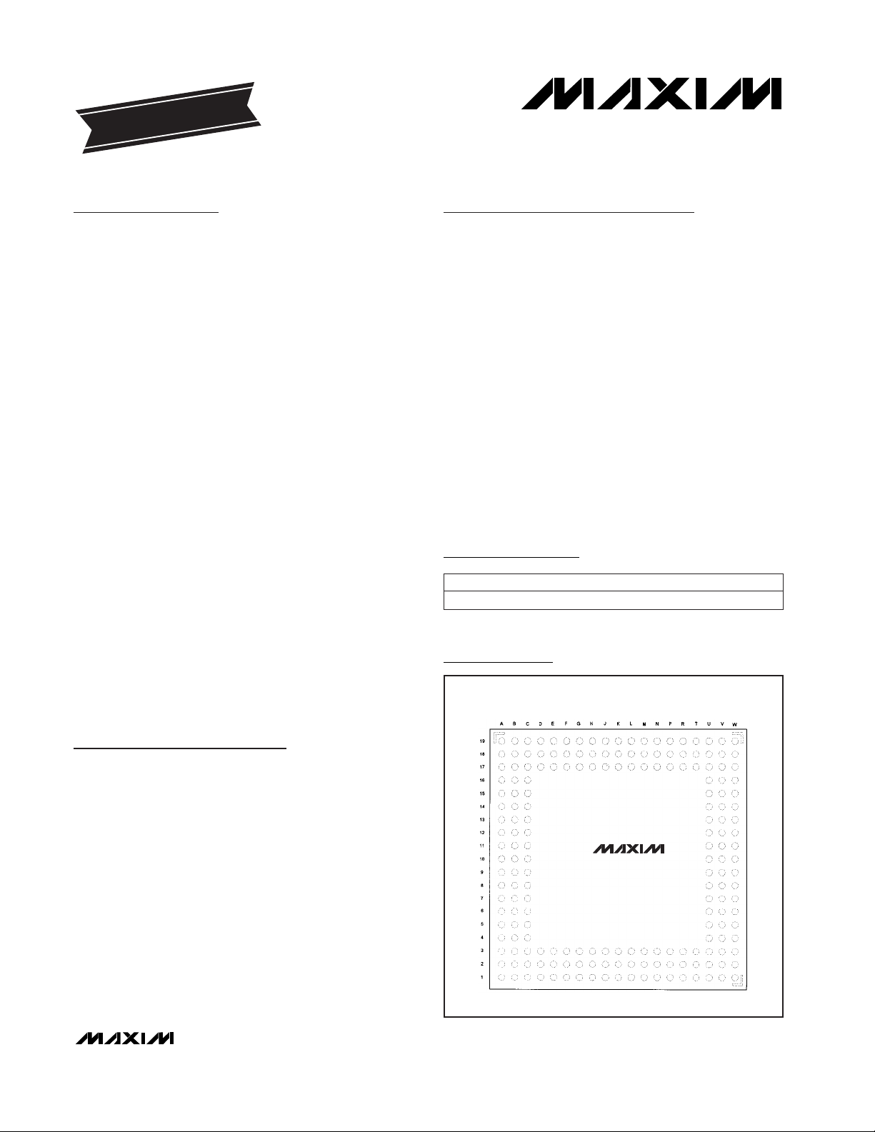
192-Contact ESBGA
Ball Assignment Matrix
Ordering Information
ESBGA is a trademark of Amkor/Anam.
MAX104
±5V, 1Gsps, 8-Bit ADC with
On-Chip 2.2GHz Track/Hold Amplifier
2 _______________________________________________________________________________________
ABSOLUTE MAXIMUM RATINGS
DC ELECTRICAL CHARACTERISTICS
(VCCA = VCCI = VCCD = +5.0V ±5%, VEE= -5.0V ±5%, VCCO = +3.0V to VCCD, REFIN connected to REFOUT, TA= T
MIN
to T
MAX
,
unless otherwise noted. Typical values are at T
A
= +25°C.)
Stresses beyond those listed under “Absolute Maximum Ratings” may cause permanent damage to the device. These are stress ratings only, and functional
operation of the device at these or any other conditions beyond those indicated in the operational sections of the specifications is not implied. Exposure to
absolute maximum rating conditions for extended periods may affect device reliability.
VCCA to GNDA.........................................................-0.3V to +6V
V
CC
D to GNDD.........................................................-0.3V to +6V
V
CC
I to GNDI............................................................-0.3V to +6V
V
CC
O to GNDD........................................-0.3V to (VCCD + 0.3V)
AUXEN1, AUXEN2 to GND .....................-0.3V to (V
CC
D + 0.3V)
V
EE
to GNDI..............................................................-6V to +0.3V
Between GNDs......................................................-0.3V to +0.3V
V
CC
A to VCCD.......................................................-0.3V to +0.3V
V
CC
A to VCCI.........................................................-0.3V to +0.3V
PECL Digital Output Current...............................................50mA
REFIN to GNDR ........................................-0.3V to (V
CC
I + 0.3V)
REFOUT Current................................................+100µA to -5mA
ICONST, IPTAT to GNDI .......................................-0.3V to +1.0V
TTL/CMOS Control Inputs (DEMUXEN,
DIVSELECT)..........................................-0.3V to (V
CC
D + 0.3V)
RSTIN+, RSTIN- ......................................-0.3V to (VCCO + 0.3V)
VOSADJ Adjust Input................................-0.3V to (V
CC
I + 0.3V)
CLK+ to CLK- Voltage Difference..........................................±3V
CLK+, CLK-.....................................(V
EE
- 0.3V) to (GNDD + 1V)
CLKCOM.........................................(V
EE
- 0.3V) to (GNDD + 1V)
VIN+ to VIN- Voltage Difference............................................±2V
VIN+, VIN- to GNDI................................................................±2V
Continuous Power Dissipation (T
A
= +70°C)
192-Contact ESBGA (derate 61mW/°C above +70°C)......4.88W
(with heatsink and 200 LFM airflow,
derate 106mW/°C above +70°C) ........................................8.48W
Operating Temperature Range
MAX104CHC........................................................0°C to +70°C
Operating Junction Temperature.....................................+150°C
Storage Temperature Range.............................-65°C to +150°C
T
A
= +25°C
Referenced to GNDR
0 < I
SOURCE
< 2.5mA
Driving REFIN input only
VIN+ and VIN- to GNDI, TA= +25°C
VOSADJ = 0 to 2.5V
Signal + offset w.r.t. GNDI
Note 1
TA= +25°C
No missing codes guaranteed
CONDITIONS
kΩ45R
REF
Reference Input Resistance
mV5∆REFOUT
Reference Output Load
Regulation
V2.475 2.50 2.525REFOUTReference Output Voltage
LSB±4 ±5.5Input VOSAdjust Range
kΩ14 25R
VOS
Input Resistance (Note 2)
LSB-0.5 ±0.25 0.5INLIntegral Nonlinearity (Note 1)
Bits8RESResolution
ppm/°C150TC
R
Input Resistance Temperature
Coefficient
Ω49 50 51R
IN
Input Resistance
V±0.8V
CM
Common-Mode Input Range
mVp-p475 500 525V
FSR
Full-Scale Input Range
LSB-0.5 ±0.25 0.5DNLDifferential Nonlinearity (Note 1)
CodesNoneMissing Codes
UNITSMIN TYP MAXSYMBOLPARAMETER
ACCURACY
ANALOG INPUTS
VOS ADJUST CONTROL INPUT
REFERENCE INPUT AND OUTPUT
MAX104
±5V, 1Gsps, 8-Bit ADC with
On-Chip 2.2GHz Track/Hold Amplifier
_______________________________________________________________________________________ 3
DC ELECTRICAL CHARACTERISTICS (continued)
(VCCA = VCCI = VCCD = +5.0V ±5%, VEE= -5.0V ±5%, VCCO = +3.0V to VCCD, REFIN connected to REFOUT, TA= T
MIN
to T
MAX
,
unless otherwise noted. Typical values are at T
A
= +25°C.)
CLK+ and CLK- to CLKCOM, TA= +25°C
VIH= 2.4V
VIL= 0
CONDITIONS
V-1.475V
IL
Digital Input Low Voltage
V-1.165V
IH
Digital Input High Voltage
µA-1 1I
IL
Low-Level Input Current
ppm/°C150TC
R
Input Resistance Temperature
Coefficient
Ω48 50 52R
CLK
Clock Input Resistance
µA50I
IH
High-Level Input Current
V0.8V
IL
Low-Level Input Voltage
V2.0V
IH
High-Level Input Voltage
UNITSMIN TYP MAXSYMBOLPARAMETER
V-1.810 -1.620V
OL
Digital Output Low Voltage
V-1.025 -0.880V
OH
Digital Output High Voltage
W5.25P
DISS
Power Dissipation (Note 6)
mA75 115ICCOOutput Supply Current (Note 6)
mA205 340ICCDDigital Supply Current
mA-290 -210I
EE
Negative Input Supply Current
mA108 150ICCIPositive Input Supply Current
mA480 780ICCAPositive Analog Supply Current
(Note 9)
VIN+ = VIN- = ±0.1V
dB40 73PSRR+
Positive Power-Supply Rejection
Ratio (Note 8)
dB40 68CMRR
Common-Mode Rejection Ratio
(Note 7)
(Note 10) dB40 68PSRR-
Negative Power-Supply
Rejection Ratio (Note 8)
CLOCK INPUTS (Note 3)
TTL/CMOS CONTROL INPUTS (DEMUXEN, DIVSELECT)
DEMUX RESET INPUT (Note 4)
PECL DIGITAL OUTPUTS (Note 5)
POWER REQUIREMENTS
MAX104
±5V, 1Gsps, 8-Bit ADC with
On-Chip 2.2GHz Track/Hold Amplifier
4 _______________________________________________________________________________________
AC ELECTRICAL CHARACTERISTICS
(VCCA = VCCI = VCCD = +5.0V, VEE= -5.0V, VCCO = +3.3V, REFIN connected to REFOUT, fS= 1Gsps, fINat -1dBFS, TA= +25°C,
unless otherwise noted.)
f
IN1
= 124MHz, f
IN2
= 126MHz,
at -7dB below full-scale
fIN= 500MHz
fIN= 1000MHz
CONDITIONS
dB-57.7IMDTwo-Tone Intermodulation
7.40
ENOB
1000
GHz2.2BW
-3dB
Analog Input Full-Power
Bandwidth
V/V1.1:1VSWRAnalog Input VSWR
7.52
UNITSMIN TYP MAXSYMBOLPARAMETER
Differential
Single-ended
fIN= 500MHz
7.49
ENOB
500
7.2 7.55Differential
Single-ended
fIN= 1000MHz
46.4
SNR
1000
46.4
fIN= 125MHz
Differential
Single-ended
Bits
7.73
ENOB
125
Effective Number of Bits
(Note 11)
7.4 7.74Differential
Single-ended
fIN= 500MHz
47.1
SNR
500
43.5 47.0Differential
Single-ended
fIN= 125MHz
dB
47.4
SNR
125
Signal-to-Noise Ratio
(No Harmonics)
44.2 47.4Differential
Single-ended
fIN= 500MHz
fIN= 1000MHz
-49.6
THD
1000
-52.6
-51.3
THD
500
Differential
Single-ended
-50 -52.5Differential
Single-ended
fIN= 125MHz
dB
-67.4
THD
125
Total Harmonic Distortion
(Note 12)
-61 -66.2Differential
Single-ended
fIN= 500MHz
fIN= 1000MHz
52.5
SFDR
1000
52.8
52.3
SFDR
500
Differential
Single-ended
50 52.3Differential
Single-ended
fIN= 125MHz
dB
69.5
SFDR
125
Spurious-Free Dynamic Range
62 68.9Differential
Single-ended
fIN= 500MHz
fIN= 1000MHz
46.3
SINAD
1000
47.0
46.9
SINAD
500
Differential
Single-ended
45.1 47.2Differential
Single-ended
fIN= 125MHz
dB
48.3
SINAD
125
Signal-to-Noise Ratio and
Distortion (Note 11)
46.3 48.3Differential
Single-ended
VOSADJ control input open LSB-1.5 0 +1.5V
OS
Transfer Curve Offset
ANALOG INPUT
DYNAMIC SPECIFICATIONS
MAX104
±5V, 1Gsps, 8-Bit ADC with
On-Chip 2.2GHz Track/Hold Amplifier
_______________________________________________________________________________________ 5
Note 1: Static linearity parameters are computed from a “best-fit” straight line through the code transition points. The full-scale
range (FSR) is defined as 256
· slope of the line.
Note 2: The offset control input is a self-biased voltage divider from the internal +2.5V reference voltage. The nominal open-circuit
voltage is +1.25V. It may be driven from an external potentiometer connected between REFOUT and GNDI.
Note 3: The clock input’s termination voltage can be operated between -2.0V and GNDI. Observe the absolute maximum ratings
on the CLK+ and CLK- inputs.
Note 4: Input logic levels are measured with respect to the V
CC
O power-supply voltage.
Note 5: All PECL digital outputs are loaded with 50Ω to V
CC
O - 2.0V. Measurements are made with respect to the VCCO power-
supply voltage.
Note 6: The current in the V
CC
O power supply does not include the current in the digital output’s emitter followers, which is a func-
tion of the load resistance and the V
TT
termination voltage.
Note 7: Common-Mode Rejection Ratio is defined as the ratio of the change in the transfer-curve offset voltage to the change in
the common-mode voltage, expressed in dB.
Note 8: Power-Supply Rejection Ratio is defined as the ratio of the change in the transfer-curve offset voltage to the change in
power-supply voltage, expressed in dB.
Note 9: Measured with the positive supplies tied to the same potential; V
CC
A = VCCD = VCCI. VCCvaries from +4.75V to +5.25V.
Note 10: V
EE
varies from -5.25V to -4.75V.
AC ELECTRICAL CHARACTERISTICS (continued)
(VCCA = VCCI = VCCD = +5.0V, VEE= -5.0V, VCCO = +3.3V, REFIN connected to REFOUT, fS= 1Gsps, fINat -1dBFS, TA= +25°C,
unless otherwise noted.)
Figure 17
20% to 80%, CL= 3pF
20% to 80%, CL= 3pF
20% to 80%, CL= 3pF
20% to 80%, CL= 3pF
Figure 15
Figure 4
Figure 4
CONDITIONS
Clock
Cycles
7.5
Primary Port Pipeline
Delay
ps180t
FDREADY
DREADY Fall Time
ps220t
RDREADY
DREADY Rise Time
ps360t
FDATA
DATA Fall Time
ns0.45t
PWL
Clock Pulse Width Low
Gsps1f
MAX
Maximum Sample Rate
ps420 t
RDATA
DATA Rise Time
ps0t
SU
Reset Input Data Setup Time
(Note 13)
ps100t
AD
Aperture Delay
ps<0.5t
AJ
Aperture Jitter
UNITSMIN TYP MAXSYMBOLPARAMETER
Figure 17 ns0.45 5t
PWH
Clock Pulse Width High
Figure 15 ps0t
HD
Reset Input Data Hold Time
(Note 13)
Figure 17 ns2.2t
PD1
CLK to DREADY Propagation
Delay
Figure 17 ps-50 150 350t
PD2
DREADY to DATA Propagation
Delay (Note 14)
8.5
Figures 6, 7, 8
Clock
Cycles
9.5
t
PDA
Auxiliary Port Pipeline
Delay
t
PDP
Figures 6, 7, 8
TIMING CHARACTERISTICS
DIV1, DIV2 modes
DIV4 mode 7.5
DIV1, DIV2 modes
DIV4 mode
MAX104
±5V, 1Gsps, 8-Bit ADC with
On-Chip 2.2GHz Track/Hold Amplifier
6 _______________________________________________________________________________________
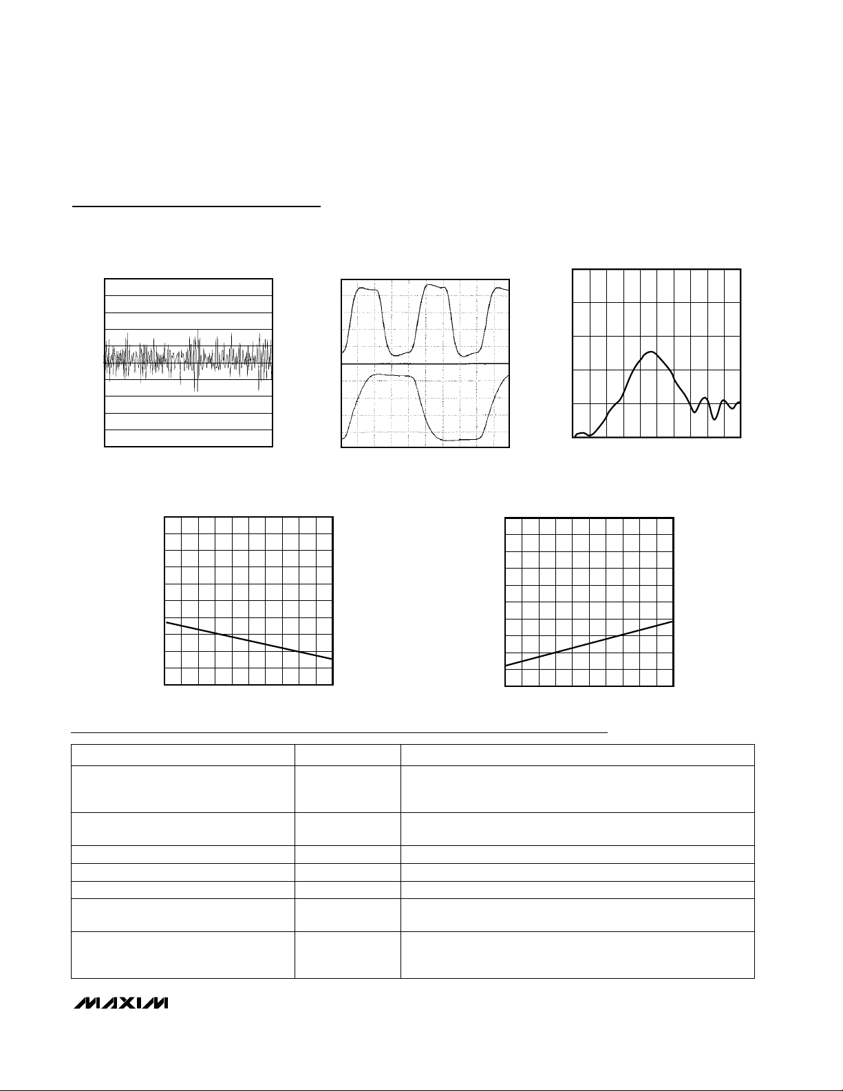
Typical Operating Characteristics
(VCCA = VCCI = VCCD = +5V, VEE= -5V, VCCO = +3.3V, REFIN connected to REFOUT, fS= 1Gsps, TA= +25°C, unless otherwise
noted.)
8.00
6.50
10 100 1000
EFFECTIVE NUMBER OF BITS vs.
ANALOG INPUT FREQUENCY
(SINGLE-ENDED ANALOG INPUT DRIVE)
6.75
7.00
7.25
7.50
7.75
MAX104toc01
ANALOG INPUT FREQUENCY (MHz)
ENOB (Bits)
-12dBFS
-6dBFS
-1dBFS
1250
8.00
6.50
10 100 1000
EFFECTIVE NUMBER OF BITS vs.
ANALOG INPUT FREQUENCY
(DIFFERENTIAL ANALOG INPUT DRIVE)
6.75
7.00
7.25
7.50
7.75
MAX104toc02
ANALOG INPUT FREQUENCY (MHz)
ENOB (Bits)
-12dBFS
-6dBFS
-1dBFS
1250
49
43
10 100 1000
SIGNAL-TO-NOISE PLUS DISTORTION vs.
ANALOG INPUT FREQUENCY
(DIFFERENTIAL ANALOG INPUT DRIVE)
44
45
46
48
47
MAX104toc04
ANALOG INPUT FREQUENCY (MHz)
SINAD (dB)
-12dBFS
-6dBFS
-1dBFS
1250
49
43
10 100
1000
SIGNAL-TO-NOISE PLUS DISTORTION vs.
ANALOG INPUT FREQUENCY
(SINGLE-ENDED ANALOG INPUT DRIVE)
44
45
46
47
48
MAX104toc03
ANALOG INPUT FREQUENCY (MHz)
SINAD (dB)
-12dBFS
-6dBFS
-1dBFS
1250
50
30
10 100
1000
SIGNAL-TO-NOISE RATIO vs.
ANALOG INPUT FREQUENCY
(SINGLE-ENDED ANALOG INPUT DRIVE)
34
38
46
42
MAX104toc05
ANALOG INPUT FREQUENCY (MHz)
SNR (dB)
-12dBFS
-6dBFS
-1dBFS
1250
50
30
10 100 1000
1250
SIGNAL-TO-NOISE RATIO vs.
ANALOG INPUT FREQUENCY
(DIFFERENTIAL ANALOG INPUT DRIVE)
34
38
46
42
MAX104toc06
ANALOG INPUT FREQUENCY (MHz)
SNR (dB)
-12dBFS
-6dBFS
-1dBFS
Note 11: Effective Number of Bits (ENOB) and Signal-to-Noise Plus Distortion (SINAD) are computed from a curve fit referenced to
the theoretical full-scale range.
Note 12: Total Harmonic Distortion (THD) is computed from the first five harmonics.
Note 13: Guaranteed by design with a reset pulse one clock period long or greater.
Note 14: The DREADY to DATA propagation delay is measured from the 50% point on the rising edge of the DREADY signal (when
the output data changes) to the 50% point on a data output bit. This places the falling edge of the DREADY signal in the
middle of the data output valid window, within the differences between the DREADY and DATA rise and fall times, which
gives maximum setup and hold time for latching external data latches.
MAX104
±5V, 1Gsps, 8-Bit ADC with
On-Chip 2.2GHz Track/Hold Amplifier
_______________________________________________________________________________________
7
80
30
10 100 1000
SPURIOUS-FREE DYNAMIC RANGE vs.
ANALOG INPUT FREQUENCY
(SINGLE-ENDED ANALOG INPUT DRIVE)
40
50
60
70
MAX104toc09
ANALOG INPUT FREQUENCY (MHz)
SFDR (dB)
-1dBFS
-6dBFS
-12dBFS
1250
80
30
10 100 1000
SPURIOUS-FREE DYNAMIC RANGE vs.
ANALOG INPUT FREQUENCY
(DIFFERENTIAL ANALOG INPUT DRIVE)
40
50
60
70
MAX104toc10
ANALOG INPUT FREQUENCY (MHz)
SFDR (dB)
-1dBFS
-6dBFS
-12dBFS
1250
6.50
7.25
7.00
6.75
7.50
7.75
8.00
4.50 4.904.70 5.10 5.30 5.50
EFFECTIVE NUMBER OF BITS
vs. V
CC
I = VCCA = VCCD
(f
IN
= 125MHz, -1dBFS)
MAX104-13
VCC (V)
ENOB (Bits)
8.00
6.50
100 1000
EFFECTIVE NUMBER OF BITS vs.
CLOCK FREQUENCY
(f
IN
= 125MHz, -1dBFS)
6.75
7.00
7.25
7.50
7.75
MAX104toc11
CLOCK FREQUENCY (MHz)
ENOB (Bits)
8.00
6.50
-12 -10
-6
-2 2 6-8 -4 0 4 108
EFFECTIVE NUMBER OF BITS vs.
CLOCK POWER
(f
IN
= 125MHz, -1dBFS)
6.75
7.00
7.25
7.50
7.75
MAX104toc12
CLOCK POWER (dBm) PER SIDE
ENOB (Bits)
SINGLE-ENDED CLOCK DRIVE
DIFFERENTIAL CLOCK DRIVE
6.50
7.25
7.00
6.75
7.50
7.75
8.00
-5.50 -5.10-5.30 -4.90 -4.70 -4.50
EFFECTIVE NUMBER OF BITS vs. V
EE
(fIN = 125MHz, -1dBFS)
MAX104-14
VEE (V)
ENOB (Bits)
55
59
57
65
63
61
67
69
73
71
75
-12 -10 -8 -6 -4 -2 0 2 4 8610
SPURIOUS-FREE DYNAMIC RANGE
vs. CLOCK POWER
(f
IN
= 125MHz, -1dBFS)
MAX104toc15
CLOCK POWER (dBm) PER SIDE
SFDR (dB)
DIFFERENTIAL CLOCK DRIVE
SINGLE-ENDED CLOCK DRIVE
Typical Operating Characteristics (continued)
(VCCA = VCCI = VCCD = +5V, VEE= -5V, VCCO = +3.3V, REFIN connected to REFOUT, fS= 1Gsps, TA= +25°C, unless otherwise
noted.)
MAX104
±5V, 1Gsps, 8-Bit ADC with
On-Chip 2.2GHz Track/Hold Amplifier
8 _______________________________________________________________________________________
Typical Operating Characteristics (continued)
(VCCA = VCCI = VCCD = +5V, VEE= -5V, VCCO = +3.3V, REFIN connected to REFOUT, fS= 1Gsps, TA= +25°C, unless otherwise
noted.)
65
67
66
69
68
71
70
72
74
73
75
4.50 4.70 4.90 5.10 5.30 5.50
SPURIOUS-FREE DYNAMIC RANGE
vs. V
CC
I = VCCA = VCCD
(f
IN
= 125MHz, -1dBFS)
MAX104-16
VCC (V)
SFDR (dB)
65
67
66
69
68
71
70
72
74
73
75
-5.50 -5.30 -5.10 -4.90 -4.70 -4.50
SPURIOUS-FREE DYNAMIC RANGE vs. V
EE
(fIN = 125MHz, -1dBFS)
MAX104-17
VEE (V)
SFDR (dB)
-128.0
-102.4
-51.2
-76.8
-25.6
0
0 200100 300 400 500
FFT PLOT
(f
IN
= 125.8545MHz, RECORD LENGTH 8192)
MAX104toc18
ANALOG INPUT FREQUENCY (MHz)
AMPLITUDE (dB)
ENOB = 7.75 BITS
SNR = 47.4dB
THD = -66.2dB
SFDR = 70.3dB
-128.0
-102.4
-51.2
-76.8
-25.6
0
0 200100 300 400 500
FFT PLOT
(f
IN
= 494.5068MHz, RECORD LENGTH 8192)
MAX104toc19
ANALOG INPUT FREQUENCY (MHz)
AMPLITUDE (dB)
ENOB = 7.51 BITS
SNR = 46.8dB
THD = -51.9dB
SFDR = 52.1dB
-5
-6
-7
-8
-9
-10
500 1500 2500
ANALOG INPUT BANDWIDTH
-6dB BELOW FULL-SCALE
MAX104toc22
ANALOG INPUT FREQUENCY (MHz)
AMPLITUDE (dB)
SMALL-SIGNAL BANDWIDTH = 2.4GHz
-128.0
-102.4
-51.2
-76.8
-25.6
0
0 200100 300 400 500
FFT PLOT
(f
IN
= 1005.0049MHz, RECORD LENGTH 8192)
MAX104toc20
ANALOG INPUT FREQUENCY (MHz)
AMPLITUDE (dB)
ENOB = 7.51 BITS
SNR = 46.3dB
THD = -52.8dB
SFDR = 53.7dB
-128.0
-76.8
-51.2
-102.4
-25.6
0
0 200100 300 400 500
TWO-TONE INTERMODULATION
FFT PLOT (f
IN1
= 124MHz, f
IN2
= 126MHz,
7dB BELOW FULL-SCALE, RECORD LENGTH 8192)
MAX104toc21
ANALOG INPUT FREQUENCY (MHz)
AMPLITUDE (dB)
f
IN1
f
IN2
0
-1
-2
-3
-4
-5
500 1500 2500
ANALOG INPUT BANDWIDTH
FULL-POWER
MAX104toc23
ANALOG INPUT FREQUENCY (MHz)
AMPLITUDE (dB)
FULL-POWER BANDWIDTH = 2.2GHz
-0.5
-0.2
-0.3
-0.4
-0.1
0
0.1
0.2
0.3
0.4
0.5
0 32 64 96 128 160 192 224 256
INTEGRAL NONLINEARITY
vs. OUTPUT CODE
(LOW-FREQUENCY SERVO LOOP DATA)
MAX104toc24
OUTPUT CODE
INL (LSB)
MAX104
±5V, 1Gsps, 8-Bit ADC with
On-Chip 2.2GHz Track/Hold Amplifier
_______________________________________________________________________________________ 9
Typical Operating Characteristics (continued)
(VCCA = VCCI = VCCD = +5V, VEE= -5V, VCCO = +3.3V, REFIN connected to REFOUT, fS= 1Gsps, TA= +25°C, unless otherwise
noted.)
Pin Description
-0.5
-0.2
-0.3
-0.4
-0.1
0
0.1
0.2
0.3
0.4
0.5
0 32 64 96 128 160 192 224 256
DIFFERENTIAL NONLINEARITY
vs. OUTPUT CODE
(LOW-FREQUENCY SERVO LOOP DATA)
MAX104toc25
OUTPUT CODE
DNL (LSB)
-70
-68
-69
-66
-67
-64
-65
-63
-61
-62
-60
-5.50 -5.30 -5.10 -4.90 -4.70 -4.50
TOTAL HARMONIC DISTORTION vs. V
EE
(f
IN
= 125MHz, -1dBFS)
MAX104-28
V
EE
(V)
THD (dB)
-70
-68
-69
-66
-67
-64
-65
-63
-61
-62
-60
4.50 4.70 4.90 5.10 5.30 5.50
TOTAL HARMONIC DISTORTION
vs. V
CC
I = VCCA = VCCD
(f
IN
= 125MHz, -1dBFS)
MAX104-29
V
CC
(V)
THD (dB)
500ps/div
DREADY RISE/FALL TIME,
DATA OUTPUT RISE/FALL TIME
DREADY
(200mV/div)
DATA
(200mV/div)
MAX104toc26
1.0
1.1
1.2
1.3
1.4
1.5
0 1000500 1500 2000 2500
VSWR vs. ANALOG INPUT FREQUENCY
MAX104toc27
ANALOG INPUT FREQUENCY (MHz)
VSWR
Test Point. Do not connect.
TESTPOINT (T.P.)A10, E17, F2, P3, R17, R18
Digital GroundGNDD
A11, B11, B16, B17, C11, C16, U9, U17,
V9, V17, V18, W9
PECL Supply Voltage, +3V to +5VVCCO
A12–A19, B19, C19, D19, E19, F19,
G19, H19, J19, K19, L19, M19, N19,
P19, T19, U19, V19, W10-W19
Analog Supply Voltage, +5V. Supplies analog comparator array.VCCAA9, B9, C9, U7, V7, W7
Analog Ground. For comparator array.GNDAA8, B8, C8, U6, V6, W6
CONTACT
Analog Supply Voltage, +5V. Supplies T/H amplifier, clock distribution, bandgap reference, and reference amplifier.
VCCIA5, B5, C5, H2, H3, M2, M3, U5, V5, W5
Analog Ground. For T/H amplifier, clock distribution, bandgap
reference, and reference amplifier.
GNDI
A1–A4, A6, A7, B1, B2, C1, C2, D1, D2,
D3, G1, H1, J2, J3, K1–K3, L2, L3, M1,
N1, T2, T3, U1, V1, V2, W1–W4
FUNCTIONNAME
MAX104
±5V, 1Gsps, 8-Bit ADC with
On-Chip 2.2GHz Track/Hold Amplifier
10 ______________________________________________________________________________________
Pin Description (continued)
CONTACT
Analog Supply Voltage, -5V. Supplies T/H amplifier, clock distribution, bandgap reference, and reference amplifier.
V
EE
B3, B4, C3, C4, E3, F3, G2, G3, N2, N3,
U2, U3, U4, V3, V4
FUNCTIONNAME
Reference Ground. Must be connected to GNDI.
GNDRB6, B7
Primary Output Data Bit 0 (LSB)P0+B12
Digital Supply Voltage, +5VVCCD
B10, B18, C10, C17, C18, T17, T18, U8,
U18, V8, W8
Primary Output Data Bit 1P1+B14
Reference InputREFINC6
Auxiliary Output Data Bit 1A1+B15
Auxiliary Output Data Bit 0 (LSB)A0+B13
Complementary Primary Output Data Bit 0 (LSB)P0-C12
Complementary Primary Output Data Bit 1P1-C14
Complementary Auxiliary Output Data Bit 0 (LSB)A0-C13
TTL/CMOS Demux Divide Selection Input
1: Decimation DIV4 mode
0: Demultiplexed DIV2 mode
DIVSELECTD17
Die Temperature Measurement Test Point. See
Die Temperature
Measurement
section.
ICONSTE1
Tie to VCCO to power the auxiliary port. Tie to GNDD to power
down.
AUXEN2D18
Complementary Auxiliary Output Data Bit 1A1-C15
Reference OutputREFOUTC7
Die Temperature Measurement Test Point. See
Die Temperature
Measurement
section.
IPTATE2
Offset Adjust InputVOSADJF1
TTL/CMOS Demux Enable Control
1: Enable Demux
0: Disable Demux
DEMUXENE18
Primary Output Data Bit 2P2+F18
Auxiliary Output Data Bit 2A2+G18
Complementary Auxiliary Output Data Bit 2A2-G17
Complementary Primary Output Data Bit 2P2-F17
Complementary Primary Output Data Bit 3P3-H17
Primary Output Data Bit 3P3+H18

MAX104
±5V, 1Gsps, 8-Bit ADC with
On-Chip 2.2GHz Track/Hold Amplifier
______________________________________________________________________________________ 11
Pin Description (continued)
Differential Input Voltage (-)VIN-J1
Auxiliary Output Data Bit 3A3+J18
Primary Output Data Bit 4P4+L18
Complementary Primary Output Data Bit 4P4-L17
Complementary Auxiliary Output Data Bit 3A3-J17
Auxiliary Output Data Bit 4A4+M18
Primary Output Data Bit 5P5+N18
Complementary Primary Output Data Bit 5P5-N17
CONTACT
Complementary Auxiliary Output Data Bit 5A5-P17
FUNCTIONNAME
This contact must be connected to GNDI.
TESTPOINT (T.P.)P2
Complementary Sampling-Clock InputCLK-P1
Complementary Auxiliary Output Data Bit 4A4-M17
Auxiliary Output Data Bit 5A5+P18
50Ω Clock Termination ReturnCLKCOMR1, R2, R3
Sampling Clock InputCLK+T1
Complementary PECL Reset OutputRSTOUT-U11
Complementary PECL Demux Reset InputRSTIN-U10
Tie to VCCO to power the auxiliary port. Tie to GNDD to power
down.
AUXEN1R19
Complementary PECL Overrange BitOR-U12
Complementary Primary Output Data Bit 7 (MSB)P7-U14
Complementary Primary Output Data Bit 6P6-U16
Complementary Auxiliary Output Data Bit 6A6-U15
Complementary Auxiliary Output Data Bit 7 (MSB)A7-U13
PECL Reset OutputRSTOUT+V11
PECL Demux Reset InputRSTIN+V10
PECL Overrange BitOR+V12
Primary Output Data Bit 7 (MSB)P7+V14
Primary Output Data Bit 6P6+V16
Auxiliary Output Data Bit 6A6+V15
Auxiliary Output Data Bit 7 (MSB)A7+V13
Complementary Data-Ready ClockDREADY-K17
Differential Input Voltage (+)VIN+L1
Data-Ready ClockDREADY+K18

MAX104
±5V, 1Gsps, 8-Bit ADC with
On-Chip 2.2GHz Track/Hold Amplifier
12 ______________________________________________________________________________________
_______________Detailed Description
The MAX104 is an 8-bit, 1Gsps flash analog-to-digital
converter (ADC) with on-chip track/hold (T/H) amplifier
and differential PECL-compatible outputs. The ADC
(Figure 1) employs a fully differential 8-bit quantizer
and a unique encoding scheme to limit metastable
states to typically one error per 1016clock cycles, with
no error exceeding 1LSB max.
An integrated 8:16 output demultiplexer simplifies interfacing to the part by reducing the output data rate to
one-half the sampling clock rate. This demultiplexer
has internal reset capability that allows multiple
MAX104s to be time-interleaved to achieve higher
effective sampling rates.
When clocked at 1Gsps, the MAX104 provides a typical effective number of bits (ENOB) of >7.5 bits at an
analog input frequency of 500MHz. The analog input of
the MAX104 is designed for differential or single-ended
use with a ±250mV full-scale input range. In addition,
this ADC features an on-chip +2.5V precision bandgap
reference. If desired, an external reference can also be
used.
CLK-
RSTIN+
RSTIN-
VOSADJ
BANDGAP
REFERENCE
+2.5V
CLK+
CLKCOM
VIN-
VIN+
REF
OUT
REF
IN
DEMUXEN
DIVSELECT
DEMUX
CLOCK
DRIVER
16
50Ω
50Ω
50Ω
50Ω
RSTOUT
A0–A7
P0–P7
DREADY
OR
DIFFERENTIAL
PECL OUTPUTS
T/H
CLOCK
DRIVER
ADC
CLOCK
DRIVER
REFERENCE
AMPLIFIER
2
2
DEMUX
CLOCK
GENERATOR
RESET INPUT
DUAL LATCH
RESET
PIPELINE
GNDI
GNDI
GNDR
DELAYED
RESET
16
16
2
2
T/H AMPLIFIER
LOGIC
CLOCK
DRIVER
BIAS CURRENTS
OVERRANGE
BIT
AUXILIARY
DATA PORT
PRIMARY
DATA PORT
DATA
READY CLOCK
DEMUX
RESET OUTPUT
8-BIT
FLASH ADC
MAX104
Figure 1. Simplified Functional Diagram

Principle of Operation
The MAX104’s flash or parallel architecture provides
the fastest multibit conversion of all common integrated
ADC designs. The key to this high-speed flash architecture is the use of an innovative, high-performance
comparator design. The flash converter and downstream logic translate the comparator outputs into a
parallel 8-bit output code and pass this binary code on
to the optional 8:16 demultiplexer, where primary and
auxiliary ports output PECL-compatible data at up to
500Msps per port (depending on how the demultiplexer section is set on the MAX104).
The ideal transfer function appears in Figure 2.
On-Chip Track/Hold Amplifier
As with all ADCs, if the input waveform is changing
rapidly during conversion, effective number of bits
(ENOB) and signal-to-noise ratio (SNR) specifications
will degrade. The MAX104’s on-chip, wide-bandwidth
(2.2GHz) T/H amplifier reduces this effect and increases
the ENOB performance significantly, allowing precise
capture of fast analog data at high conversion rates.
The T/H amplifier buffers the input signal and allows a
full-scale signal input range of ±250mV. The T/H amplifier’s differential 50Ω input termination simplifies interfacing to the MAX104 with controlled impedance lines.
Figure 3 shows a simplified diagram of the T/H amplifier
stage internal to the MAX104.
Aperture width, delay, and jitter (or uncertainty) are
parameters that affect the dynamic performance of
high-speed converters. Aperture jitter, in particular,
directly influences SNR and limits the maximum slew
rate (dV/dt) that can be digitized without contributing
significant errors. The MAX104’s innovative T/H amplifier
design limits aperture jitter typically to less than 0.5ps.
Aperture Width
Aperture width (tAW) is the time the T/H circuit requires
(Figure 4) to disconnect the hold capacitor from the
input circuit (for instance, to turn off the sampling
bridge and put the T/H unit in hold mode).
Aperture Jitter
Aperture jitter (tAJ) is the sample-to-sample variation
(Figure 4) in the time between the samples.
Aperture Delay
Aperture delay (tAD) is the time defined between the
rising edge of the sampling clock and the instant when
an actual sample is taken (Figure 4).
Internal Reference
The MAX104 features an on-chip +2.5V precision
bandgap reference, which can be used by connecting
MAX104
±5V, 1Gsps, 8-Bit ADC with
On-Chip 2.2GHz Track/Hold Amplifier
______________________________________________________________________________________ 13
(-FS + 1LSB)
0
+FS
(+FS - 1LSB)
255
255
254
129
128
127
126
3
2
1
0
ANALOG INPUT
OVERRANGE +
DIGITAL OUTPUT
Figure 2. Transfer Function
HOLD
CLK
ANALOG
INPUT
SAMPLED
DATA (T/H)
T/H
t
AW
t
AD
t
AJ
TRACK TRACK
APERTURE DELAY (t
AD
)
APERTURE WIDTH (t
AW
)
APERTURE JITTER (t
AJ
)
CLK
Figure 4. T/H Aperture Timing
TO
COMPARATORS
TO
COMPARATORS
BUFFER
AMPLIFIER
INPUT
AMPLIFIER
CLOCK
SPLITTER
ALL INPUTS ARE ESD PROTECTED
(NOT SHOWN IN THIS
SIMPLIFIED DRAWING).
SAMPLING
BRIDGE
GNDI
50Ω50Ω
VIN+
VIN-
GNDI
C
HOLD
50Ω50Ω
CLK+
CLK-
CLKCOM
Figure 3. Internal Structure of the 2.2GHz T/H Amplifier

MAX104
REFOUT to REFIN. This connects the reference output
to the positive input of the reference buffer. The buffer’s
negative input is internally connected to GNDR. GNDR
must be connected to GNDI on the user’s application
board. REFOUT can source up to 2.5mA to supply
external devices if required.
An adjustable external reference can be used to adjust
the ADC’s full-scale range. To use an external reference supply, simply connect a high-precision reference
to the REFIN pin and leave the REFOUT pin floating. In
this configuration, REFOUT must not be simultaneously
connected to avoid conflicts between the two references. REFIN has a typical input resistance of 5kΩ and
accepts input voltages of +2.5V ±200mV. Using the
MAX104’s internal reference is recommended for best
performance.
Digital Outputs
The MAX104 provides data in offset binary format to differential PECL outputs. A simplified circuit schematic of
the PECL output cell is shown in Figure 5. All PECL outputs are powered from VCCO, which may be operated
from any voltage between +3.0V to VCCD for flexible
interfacing with either +3.3V or +5V systems. The nominal VCCO supply voltage is +3.3V.
All PECL outputs on the MAX104 are open-emitter
types and must be terminated at the far end of each
transmission line with 50Ω to VCCO - 2V. Table 1 lists all
MAX104 PECL outputs and their functions.
Demultiplexer Operation
The MAX104 features an internal data demultiplexer
that provides for three different modes of operation (see
the following sections on
Demultiplexed DIV2 Mode,
Non-Demultiplexed DIV1 Mode,
and
Decimation DIV4
Mode
) controlled by two TTL/CMOS-compatible inputs:
DEMUXEN and DIVSELECT.
DEMUXEN enables or disables operation of the internal
1:2 demultiplexer. A logic high on DEMUXEN activates
the internal demultiplexer, and a logic low deactivates
it. With the internal demultiplexer enabled, DIVSELECT
controls the selection of the operational mode. DIVSELECT low selects demultiplexed DIV2 mode, and DIVSELECT high selects decimation DIV4 mode (Table 2).
±5V, 1Gsps, 8-Bit ADC with
On-Chip 2.2GHz Track/Hold Amplifier
14 ______________________________________________________________________________________
Auxiliary-Port Differential Outputs from LSB to MSB. A “+” indicates the true outputs; a “-”
denotes the complementary outputs.
A0+, A0-, A1+, A1-, A2+, A2-,
A3+, A3-, A4+, A4-, A5+, A5-,
A6+, A6-, A7+, A7-
Overrange True and Complementary OutputsOR+, OR-
Data-Ready Clock True and Complementary Outputs. These signal lines are used to latch
the output data from the primary to the auxiliary output ports. Data changes on the rising
edge of the DREADY clock.
DREADY+, DREADY-
Reset Output True and Complementary OutputsRSTOUT+, RSTOUT-
PECL OUTPUT SIGNALS
Primary-Port Differential Outputs from LSB to MSB. A “+” indicates the true outputs; a “-”
denotes the complementary outputs.
P0+, P0-, P1+, P1-, P2+, P2-,
P3+, P3-, P4+, P4-, P5+, P5-,
P6+, P6-, P7+, P7-
FUNCTIONAL DESCRIPTION
Figure 5. Simplified PECL Output Structure
Table 1. PECL Output Functions
500Ω 500Ω
DIFF.
PAIR
1.8mA
GNDD GNDD
V
CC
A_+/P_+
GNDD
A_-/P_-
O

Non-Demultiplexed DIV1 Mode
The MAX104 may be operated at up to 500Msps in nondemultiplexed DIV1 mode (Table 2). In this mode, the
internal demultiplexer is disabled, and sampled data is
presented to the primary port only, with the data repeated at the auxiliary port but delayed by one clock cycle
(Figure 6). Since the auxiliary output port contains the
same data stream as the primary output port, the auxiliary port can be shut down to save power by connecting
AUXEN1 and AUXEN2 to digital ground (GNDD). This
powers down the internal bias cells and causes both
outputs (true and complementary) of the auxiliary port to
pull up to a logic-high level. To save additional power,
the external 50Ω termination resistors connected to the
PECL termination power supply (V
CC
O - 2V) may be
removed from all auxiliary output ports.
Demultiplexed DIV2 Mode
The MAX104 features an internally selectable DIV2
mode (Table 2) that reduces the output data rate to
one-half of the sample clock rate. The demultiplexed
outputs are presented in dual 8-bit format with two consecutive samples appearing in the primary and auxiliary output ports on the rising edge of the data-ready
clock (Figure 7). The auxiliary data port contains the
previous sample, and the primary output contains the
most recent data sample. AUXEN1 and AUXEN2 must
be connected to VCCO to power-up the auxiliary port
PECL output drivers.
MAX104
±5V, 1Gsps, 8-Bit ADC with
On-Chip 2.2GHz Track/Hold Amplifier
______________________________________________________________________________________ 15
NOTE: THE AUXILIARY PORT DATA IS DELAYED ONE ADDITIONAL CLOCK CYCLE FROM THE PRIMARY PORT DATA.
GROUNDING AUXEN1 AND AUXEN2 WILL POWER DOWN THE AUXILIARY PORT TO SAVE POWER.
CLK-
CLK+
n n+1 n+2 n+3 n+4 n+5
n+1 n+2 n+3 n+4
n n+1 n+2 n+3 n+4
n+5
n+6 n+7 n+8 n+9 n+10 n+11 n+12 n+13
ADC SAMPLE NUMBER
ADC SAMPLES ON THE RISING EDGE OF CLK+
CLK
DREADY
AUXILIARY
DATA PORT
PRIMARY
DATA PORT
DREADY+
DREADY-
Figure 6. Non-Demuxed, DIV1-Mode Timing Diagram
NOTE: THE LATENCY TO THE PRIMARY PORT IS 7.5 CLOCK CYCLES, AND THE LATENCY TO THE AUXILIARY PORT IS 8.5 CLOCK CYCLES.
BOTH THE PRIMARY AND AUXILIARY DATA PORTS ARE UPDATED ON THE RISING EDGE OF THE DREADY+ CLOCK.
CLK-
CLK+
n n+1 n+2 n+3 n+4 n+5
n+1n-1 n+3
n+6 n+7 n+8 n+9 n+10 n+11 n+12 n+13
ADC SAMPLE NUMBER
ADC SAMPLES ON THE RISING EDGE OF CLK+
CLK
DREADY
AUXILIARY
DATA PORT
PRIMARY
DATA PORT
DREADY+
DREADY-
n n+2 n+4
Figure 7. Demuxed DIV2-Mode Timing Diagram

MAX104
Decimation DIV4 Mode
The MAX104 also offers a special decimated, demultiplexed output (Figure 8) that discards every other input
sample and outputs data at one-quarter the input sampling rate for system debugging at slower output data
rates. With an input clock of 1GHz, the effective output
data rate will be reduced to 250MHz per output port in
the DIV4 mode (Table 2). Since every other sample is
discarded, the effective sampling rate is 500Msps.
Overrange Operation
A single differential PECL overrange output bit (OR+,
OR-) is provided for both primary and auxiliary demultiplexed outputs. The operation of the overrange bit
depends on the status of the internal demultiplexer. In
demultiplexed DIV2 mode and decimation DIV4 mode,
the OR bit will flag an overrange condition if either the
primary or auxiliary port contains an overranged sample (Table 2). In non-demultiplexed DIV1 mode, the OR
port will flag an overrange condition only when the primary output port contains an overranged sample.
Applications Information
Single-Ended Analog Inputs
The MAX104 T/H amplifier is designed to work at full
speed for both single-ended and differential analog
inputs (Figure 9). Inputs VIN+ and VIN- feature on-chip,
laser-trimmed 50Ω termination resistors to provide
excellent voltage standing wave ratio (VSWR) performance.
±5V, 1Gsps, 8-Bit ADC with
On-Chip 2.2GHz Track/Hold Amplifier
16 ______________________________________________________________________________________
NOTE: THE LATENCY TO THE PRIMARY PORT REMAINS 7.5 CLOCK CYCLES, WHILE THE LATENCY OF THE AUXILIARY PORT INCREASES TO 9.5 CLOCK CYCLES.
THIS EFFECTIVELY DISCARDS EVERY OTHER SAMPLE AND REDUCES THE OUTPUT DATA RATE TO 1/4 THE SAMPLE CLOCK RATE.
CLK-
CLK+
n n+1 n+2 n+3 n+4 n+5
n-2 n+2
n+6 n+7 n+8 n+9 n+10 n+11 n+12 n+13
ADC SAMPLE NUMBER
ADC SAMPLES ON THE RISING EDGE OF CLK+
CLK
DREADY
AUXILIARY
DATA PORT
PRIMARY
DATA PORT
DREADY+
DREADY-
n
n+4
Figure 8. Decimation DIV4-Mode Timing Diagram
Table 2. Demultiplexer Operation
Flags overrange data appearing in primary
port only.
Low
High
DEMUXEN OVERRANGE BIT OPERATION
X
Low
DIVSELECT
DIV1
500Msps (max)
DIV2
500Msps/port
DEMUX MODE
High
Flags overrange data appearing in either
the primary or auxiliary port.
High
DIV4
250Msps/port
X = Don’t care

In a typical single-ended configuration, the analog
input signal (Figure 10a) enters the T/H amplifier stage
at the in-phase input (VIN+), while the inverted phase
input (VIN-) is reverse-terminated to GNDI with an
external 50Ω resistor. Single-ended operation allows for
an input amplitude of ±250mV. Table 3 shows a selection of input voltages and their corresponding output
codes for single-ended operation.
Differential Analog Inputs
To obtain a full-scale digital output with differential input
drive (Figure 10b), 250mVp-p must be applied between
VIN+ and VIN- (VIN+ = +125mV and VIN- = -125mV).
Midscale digital output codes (01111111 or 10000000)
occur when there is no voltage difference between
VIN+ and VIN-. For a zero-scale digital output code, the
in-phase (VIN+) input must see -125mV and the inverted input (VIN-) must see +125mV. A differential input
drive is recommended for best performance. Table 4
represents a selection of differential input voltages and
their corresponding output codes.
MAX104
±5V, 1Gsps, 8-Bit ADC with
On-Chip 2.2GHz Track/Hold Amplifier
______________________________________________________________________________________ 17
+2.8V
50Ω
50Ω
VIN+
ANALOG INPUTS ARE ESD PROTECTED
(NOT SHOWN IN THIS SIMPLIFIED DRAWING).
VIN-
GNDI
V
EE
Figure 9. Simplified Analog Input Structure (Single-Ended/
Differential)
V
IN+
V
IN-
OV
+250mV
-250mV
t
500mVp-p
FS ANALOG
INPUT RANGE
V
IN
= ±250mV
500mV
Figure 10a. Single-Ended Analog Input Signals
V
IN+
V
IN-
+125mV
-125mV
t
±250mV
FS ANALOG
INPUT RANGE
OV
250mV
-250mV
Figure 10b. Differential Analog Input Signals
Table 3. Ideal Input Voltage and Output Code Results for Single-Ended Operation
0V 11111111 (full scale)+250mV
VIN-
1
OVERRANGE BITVIN+ OUTPUT CODE
0V 11111111+250mV - 1LSB 0
0V
0V
01111111
toggles
10000000
0V 0
0000001 -250mV + 1LSB 0
0V 00000000 (zero scale)-250mV 0

MAX104
Offset Adjust
The MAX104 provides a control input (VOSADJ) to compensate for system offsets. The offset adjust input is a
self-biased voltage divider from the internal +2.5V precision reference. The nominal open-circuit voltage is onehalf the reference voltage. With an input resistance of
typically 25kΩ, this pin may be driven by an external
10kΩ potentiometer (Figure 11) connected between
REFOUT and GNDI to correct for offset errors. This control provides a typical ±5.5LSB offset adjustment range.
Clock Operation
The MAX104 clock inputs are designed for either singleended or differential operation (Figure 12) with flexible
input drive requirements. Each clock input is terminated
with an on-chip, laser-trimmed 50Ω resistor to CLKCOM
(clock-termination return). The CLKCOM termination
voltage can be connected anywhere between ground
and -2V for compatibility with standard ECL drive levels.
The clock inputs are internally buffered with a preamplifier to ensure proper operation of the data converter
with even small-amplitude sine-wave sources. The
MAX104 was designed for single-ended, low-phasenoise sine-wave clock signals with as little as 100mV
amplitude (-10dBm). This eliminates the need for an
external ECL clock buffer and its added jitter.
Single-Ended Clock Inputs (Sine-Wave Drive)
Excellent performance is obtained by AC- or DC-coupling a low-phase-noise sine-wave source into a single
clock input (Figure 13a, Table 5). For proper DC balance, the undriven clock input should be externally
50Ω reverse-terminated to GNDI.
The dynamic performance of the data converter is
essentially unaffected by clock-drive power levels from
±5V, 1Gsps, 8-Bit ADC with
On-Chip 2.2GHz Track/Hold Amplifier
18 ______________________________________________________________________________________
Table 4. Ideal Input Voltage and Output Code Results for Differential Operation
-125mV
-125mV + 0.5LSB
11111111 (full scale)+125mV
VIN-
1
11111111+125mV - 0.5LSB 0
OVERRANGE BIT
0V
+125mV - 0.5LSB
01111111
toggles
10000000
0V 0
00000001-125mV + 0.5LSB 0
+125mV 00000000 (zero scale)-125mV 0
VIN+ OUTPUT CODE
Figure 11. Offset Adjust with External 10kΩPotentiometer
CLK+
CLKCOM
CLOCK INPUTS ARE
ESD PROTECTED
(NOT SHOWN IN THIS
SIMPLIFIED DRAWING).
CLK-
50Ω
+0.8V
50Ω
GNDI
V
EE
Figure 12. Simplified Clock Input Structure (Single-Ended/
Differential)
REFOUT
POT
10k
GNDI
MAX104
VOSADJ

-10dBm (100mV clock signal amplitude) to +10dBm
(1V clock signal amplitude). The MAX104 dynamic performance specifications are determined by a singleended clock drive of +4dBm (500mV clock signal
amplitude). To avoid saturation of the input amplifier
stage, limit the clock power level to a maximum of
+10dBm.
Differential Clock Inputs (Sine-Wave Drive)
The advantages of differential clock drive (Figure 13b,
Table 5) can be obtained by using an appropriate
balun or transformer to convert single-ended sine-wave
sources into differential drives. The precision on-chip,
laser-trimmed 50Ω clock-termination resistors ensure
excellent amplitude matching. Refer to
Single-Ended
Clock Inputs (Sine-Wave Drive)
for proper input ampli-
tude requirements.
Single-Ended Clock Inputs (ECL Drive)
Configure the MAX104 for single-ended ECL clock drive
by connecting the clock inputs as shown in Figure 13c
(Table 5). A well bypassed VBBsupply (-1.3V) is essential to avoid coupling noise into the undriven clock input,
which would degrade dynamic performance.
Differential Clock Inputs (ECL Drive)
The MAX104 may be driven from a standard differential
(Figure 13d, Table 5) ECL clock source by setting the
clock termination voltage at CLKCOM to -2V. Bypass
the clock-termination return (CLKCOM) as close as
possible to the ADC with a 0.01µF capacitor connected
to GNDI.
AC-Coupling Clock Inputs
The clock inputs CLK+ and CLK- can also be driven
with positive referenced ECL (PECL) logic if the clock
MAX104
±5V, 1Gsps, 8-Bit ADC with
On-Chip 2.2GHz Track/Hold Amplifier
______________________________________________________________________________________ 19
CLK+
CLK- = 0V
+0.5V
-0.5V
NOTE: CLKCOM = 0V
t
Figure 13a. Single-Ended Clock Input Signals
CLK+
-0.8V
-1.8V
t
CLK- = -1.3V
NOTE: CLKCOM = -2V
Figure 13c. Single-Ended ECL Clock Drive
CLK+
CLK-
+0.5V
-0.5V
t
NOTE: CLKCOM = 0V
Figure 13b. Differential Clock Input Signals
CLK+
CLK-
-0.8V
-1.8V
t
NOTE: CLKCOM = -2V
Figure 13d. Differential ECL Clock Drive

MAX104
inputs are AC-coupled. Under this condition, connect
CLKCOM to GNDI. Single-ended ECL/PECL/sine-wave
drive is also possible if the undriven clock input is
reverse-terminated to GNDI through a 50Ω resistor in
series with a capacitor whose value is identical to that
used to couple the driven input.
Demux Reset Operation
The MAX104 features an internal 1:2 demultiplexer that
reduces the data rate of the output digital data to onehalf the sample clock rate. Demux reset is necessary
when interleaving multiple MAX104s and/or synchronizing external demultiplexers. The simplified block diagram
of Figure 1 shows that the demux reset signal path consists of four main circuit blocks. From input to output,
they are the reset input dual latch, the reset pipeline, the
demux clock generator, and the reset output. The signals associated with the demux reset operation and the
control of this section are listed in Table 6.
Reset Input Dual Latch
The reset input dual-latch circuit block accepts differential PECL reset inputs referenced to the same VCCO
power supply that powers the MAX104 PECL outputs.
For applications that do not require a synchronizing
reset, the reset inputs can be left open. In this case,
they will self-bias to a proper level with internal 50kΩ
resistors and 20µA current source. This combination
creates a -1V difference between RSTIN+ and RSTINto disable the internal reset circuitry. When driven with
PECL logic levels terminated with 50Ω to (VCCO - 2V),
the internal biasing network can easily be overdriven.
Figure 14 shows a simplified schematic of the reset
input structure.
To properly latch the reset input data, the setup time
(tSU) and the data hold time (tHD) must be met with
respect to the rising edge of the sample clock. The timing diagram of Figure 15 shows the timing relationship
of the reset input and sampling clock.
±5V, 1Gsps, 8-Bit ADC with
On-Chip 2.2GHz Track/Hold Amplifier
20 ______________________________________________________________________________________
Table 5. DC-Coupled Clock Drive Options
-10dBm to +4dBm Figure 13aSingle-Ended Sine Wave
CLK+
GNDI
CLKCOMCLOCK DRIVE REFERENCE
External 50Ω to GNDI
CLK-
-10dBm to +4dBm -10dBm to +4dBm Figure 13bDifferential Sine Wave GNDI
ECL Drive -1.3V Figure 13cSingle-Ended ECL -2V
ECL Drive
ECL Drive
Figure 13dDifferential ECL -2V
Figure 14. Simplified Reset Input Structure
RSTIN+
50% 50%
CLK+
CLK-
RSTIN-
50%
t
SU
t
HD
Figure 15. Reset Input Timing Definitions
RSTIN+
RSTIN-
V
50k50k
20µA
O
CC
RESET INPUTS ARE
ESD PROTECTED
(NOT SHOWN IN THIS
SIMPLIFIED DRAWING).
GNDD

Reset Pipeline
The next section in the reset signal path is the reset
pipeline. The purpose of this block is to add clock
cycles of latency to the reset signal, to match the latency of the converted analog data through the ADC. In
this way, when reset data arrives at the RSTOUT+/
RSTOUT- PECL output, it will be time-aligned with the
analog data present in the primary and auxiliary ports
at the time the reset input was deasserted at RSTIN+/
RSTIN-.
Demux Clock Generator
The demux clock generator creates the DIV1, DIV2, or
DIV4 clocks required for the different modes of demux
and non-demux operation. The TTL/CMOS control
inputs DEMUXEN and DIVSELECT control the demuxed
mode selection, as described in Table 2. The timing
diagrams in Figure 16 and Figure 17 show the output
timing and data alignment in DIV1, DIV2, and DIV4
modes, respectively.
The phase relationship between the sampling clock at
the CLK+/CLK- inputs and the data-ready clock at the
DREADY+/DREADY- outputs will be random at device
power-up. As with all divide-by-two circuits, two possible phase relationships exist between these clocks.
The difference between the phases is simply the inversion of the DIV2-DREADY clock. The timing diagram in
Figure 16 shows this relationship.
Reset all MAX104 devices to a known DREADY phase
after initial power-up for applications such as interleaving, where two or more MAX104 devices are used to
achieve higher effective sampling rates. This synchronization is necessary to set the order of output samples
between the devices. Resetting the converters accomplishes this synchronization. The reset signal is used to
force the internal counter in the demux clock-generator
block to a known phase state.
MAX104
±5V, 1Gsps, 8-Bit ADC with
On-Chip 2.2GHz Track/Hold Amplifier
______________________________________________________________________________________ 21
Table 6. Demux Operating and Reset Control Signal
50%
CLK+
CLK-
DREADY +
DREADY -
"PHASE 1"
"PHASE 2"
20% 20%
50%
80% 80%
t
PD1
DREADY-
DREADY+
t
RDREADY
t
FDREADY
Figure 16. CLK and DREADY Timing in Demuxed DIV2 Mode
Showing Two Possible DREADY Phases
CLK+
CLK-
DREADY +
DREADY -
AUXILIARY PORT DATA
PRIMARY PORT DATA
t
PWH
t
PWL
t
PD1
t
PD2
Figure 17. Output Timing for All Modes (DIV1, DIV2, DIV4)
Sampling clock inputs Master ADC timing signal. The ADC samples on the rising edge of CLK+.CLK+, CLK-
TYPE
Differential PECL outputs
Data-Ready PECL Output. Output data changes on the rising edge of
DREADY+.
DREADY+, DREADY-
Differential PECL inputs Demux reset input signals. Resets the internal demux when asserted.RSTIN+, RSTINDifferential PECL outputs Reset outputs for resetting additional external demux devicesRSTOUT+, RSTOUT-
SIGNAL NAME FUNCTION

MAX104
Reset Output
Finally, the reset signal is presented in differential PECL
format to the last block of the reset signal path.
RSTOUT+/RSTOUT- output the time-aligned reset signal used for resetting additional external demuxes in
applications that need further output data rate reduction. Many demux devices require that their reset signal
be asserted for several clock cycles while they are
clocked. To accomplish this, the MAX104 DREADY
clock will continue to toggle while RSTOUT is asserted.
When a single MAX104 device is used, no synchronizing reset is required, because the order of the samples
in the output ports is unchanged regardless of the
phase of the DREADY clock. In DIV2 mode, the data in
the auxiliary port is delayed by 8.5 clock cycles, while
the data in the primary port is delayed by 7.5 clock
cycles. The older data is always in the auxiliary port,
regardless of the phase of the DREADY clock.
The reset output signal, RSTOUT, is delayed by one
less clock cycle (6.5 clock cycles) than the primary
port. The reduced latency of RSTOUT serves to mark
the start of synchronized data in the primary and auxiliary ports. When the RSTOUT signal returns to a zero,
the DREADY clock phase is reset.
Since there are two possible phases of the DREADY
clock with respect to the input clock, there are two possible timing diagrams to consider. The first timing diagram (Figure 18) shows the RSTOUT timing and data
alignment of the auxiliary and primary output ports
when the DREADY clock phase is already reset. For
this example, the RSTIN pulse is two clock cycles long.
Under this condition, the DREADY clock continues
uninterrupted, as does the data stream in the auxiliary
and primary ports.
The second timing diagram (Figure 19) shows the
results when the DREADY phase is opposite from the
reset phase. In this case, the DREADY clock “swallows”
a clock cycle of the sample clock, resynchronizing to
the reset phase. Note that the data stream in the auxiliary and primary ports has reversed. Before reset was
±5V, 1Gsps, 8-Bit ADC with
On-Chip 2.2GHz Track/Hold Amplifier
22 ______________________________________________________________________________________
NOTE: THE LATENCY TO THE RESET OUTPUT IS 6.5 CLOCK CYCLES. THE LATENCY TO THE PRIMARY PORT IS 7.5 CLOCK CYCLES, AND
THE LATENCY TO THE AUXILIARY PORT IS 8.5 CLOCK CYCLES. ALL DATA PORTS ARE UPDATED ON THE RISING EDGE OF THE DREADY+ CLOCK.
CLK-
CLK+
t
SU
t
HD
n n+1 n+2 n+3 n+4 n+5 n+6 n+7 n+8 n+9 n+10 n+11 n+12 n+13
ADC SAMPLE NUMBER
ADC SAMPLES ON THE RISING EDGE OF CLK+
CLK
DREADY
DREADY+
DREADY-
RSTIN+
RSTIN-
RSTOUT+
RSTOUT-
RESET
INPUT
n+1n-1 n+3
AUXILIARY
DATA PORT
PRIMARY
DATA PORT
n n+2 n+4
RESET OUT
DATA PORT
Figure 18. Reset Output Timing in Demuxed DIV2 Mode (DREADY Aligned)

asserted, the auxiliary port contained “even” samples
while the primary port contained “odd” samples. After
the RSTOUT is deasserted (which marks the start of the
DREADY clock’s reset phase), note that the order of the
samples in the ports has been reversed. The auxiliary
port also contains an out-of-sequence sample. This is a
consequence of the “swallowed” clock cycle that was
needed to resynchronize DREADY to the reset phase.
Also note that the older sample data is always in the auxiliary port, regardless of the DREADY phase.
These examples illustrate the combinations that result
with a reset input signal of two clock cycles. It is also
possible to reset the internal MAX104 demux successfully with a reset pulse of only one clock cycle, provided
that the setup-time and hold-time requirements are met
with respect to the sample clock. However, this is not
recommended when additional external demuxes are
used.
Note that many external demuxes require that their
reset signals be asserted while they are clocked, and
may require more than one clock cycle of reset. More
importantly, if the phase of the DREADY clock is such
that a clock pulse will be “swallowed” to resynchronize,
then no reset output will occur at all. In effect, the
RSTOUT signal will be “swallowed” with the clock
pulse. The best method to ensure complete system
reset is to assert RSTIN for the appropriate number of
DREADY clock cycles required to complete reset of the
external demuxes.
Die Temperature Measurement
For applications that require monitoring of the die temperature, it is possible to determine the die temperature
of the MAX104 under normal operating conditions by
observing the currents I
CONST
and I
PTAT
, at contacts
ICONST and IPTAT. I
CONST
and I
PTAT
are two 100µA
(nominal) currents that are designed to be equal at
+27°C. These currents are derived from the MAX104’s
internal precision +2.5V bandgap reference. I
CONST
is
designed to be temperature independent, while I
PTAT
is
directly proportional to the absolute temperature. These
currents are derived from pnp current sources referenced from VCCI and driven into two series diodes connected to GNDI. The contacts ICONST and IPTAT may
be left open, because internal catch diodes prevent
saturation of the current sources. The simplest method
MAX104
±5V, 1Gsps, 8-Bit ADC with
On-Chip 2.2GHz Track/Hold Amplifier
______________________________________________________________________________________ 23
NOTE: DREADY PHASE WAS ADJUSTED TO MATCH THE RESET PHASE BY “SWALLOWING” ONE INPUT CLOCK CYCLE.
THE AUXILIARY PORT CONTAINS AN OUT-OF-SEQUENCE SAMPLE AS A RESULT OF THE DELAY.
CLK-
CLK+
t
SU t
HD
n n+1 n+2 n+3 n+4 n+5 n+6 n+7 n+8 n+9 n+10 n+11 n+12 n+13
ADC SAMPLE NUMBER
ADC SAMPLES ON THE RISING EDGE OF CLK+
CLOCK PULSE “SWALLOWED”
OUT-OF-SEQUENCE SAMPLE
CLK
DREADY
DREADY+
DREADY-
RSTIN+
RSTIN-
RSTOUT+
RSTOUT-
RESET
INPUT
n-1 n+1
n-2
AUXILIARY
DATA PORT
PRIMARY
DATA PORT
n
n+2
n+4
RESET OUT
DATA PORT
Figure 19. Reset Output Timing in Demuxed DIV2 Mode (DREADY Realigned)

MAX104
of determining the die temperature is to measure each
current with an ammeter (which shuts off the internal
catch diodes) referenced to GNDI. The die temperature
in °C is then calculated by the expression:
Another method of determining the die temperature
uses the operational amplifier circuit shown in Figure 20.
The circuit produces a voltage that is proportional to
the die temperature. A possible application for this signal is speed control for a cooling fan, to maintain constant MAX104 die temperature. The circuit operates by
converting the I
CONST
and I
PTAT
currents to voltages
V
CONST
and V
PTAT
, with appropriate scaling to account
for their equal values at +27°C. This voltage difference
is then amplified by two amplifiers in an instrumentation-amplifier configuration with adjustable gain. The
nominal value of the circuit gain is 4.5092V/V. The gain
of the instrumentation amplifier is given by the expression:
To calibrate the circuit, first connect pins 2-3 on JU1 to
zero the input of the PTAT path. With the MAX104 powered up, adjust potentiometer R3 until the voltage at the
V
TEMP
output is -2.728V. Connecting pins 1-2 on JU1
restores normal operation to the circuit after the calibration is complete. The voltage at the V
TEMP
node will
then be proportional to the actual MAX104 die temperature according to the equation:
T
DIE
(°C) = 100 · V
TEMP
The overall accuracy of the die temperature measurement using the operational-amplifier scaling circuitry is
limited mainly by the accuracy and matching of the
resistors in the circuit.
Thermal Management
Depending on the application environment for the
ESBGA-packaged MAX104, the customer may have to
apply an external heatsink to the package after board
assembly. Existing open-tooled heatsinks are available
from standard heatsink suppliers (see
Heatsink
Manufacturers
). The heatsinks are available with pre-
applied adhesive for easy package mounting.
A
V
VV
A
R
R
R
R
V
TEMP
CONST PTAT
V
=
−
=+ +
⋅1
1
2
2
1
3
T
I
I
DIE
PTAT
CONST
=
−⋅300 273
±5V, 1Gsps, 8-Bit ADC with
On-Chip 2.2GHz Track/Hold Amplifier
24 ______________________________________________________________________________________
V
CONST
V
TEMP
R1
7.5k
R2
15k
R2
15k
3.32k
5k
R1
7.5k
6.65k
6.65k
6.05k
12.1k
12.1k
1
2
3
JU1
10-TURN
I
PTAT
V
PTAT
I
CONST
1/4 MAX479
1/4 MAX479
1/4 MAX479
1/4 MAX479
Figure 20. Die Temperature Acquisition Circuit with the MAX479

Thermal Performance
The MAX104 has been modeled to determine the thermal resistance from junction to ambient. Table 7 lists
the ADC’s thermal performance parameters:
Ambient Temperature: TA= +70°C
Heatsink Dimensions: 25mm x 25mm x 10mm
PC Board Size and Layout: 4" x 4"
2 Signal Layers
2 Power Layers
Heatsink Manufacturers
Aavid Engineering and IERC provide open-tool, lowprofile heatsinks, fitting the 25mm x 25mm ESBGA
package.
Aavid Engineering, Inc.
Phone: 714-556-2665
Heatsink Catalog #: 335224B00032
Heatsink Dimensions: 25mm x 25mm x 10mm
International Electronic Research Corporation (IERC)
Phone: 818-842-7277
Heatsink Catalog #: BDN09-3CB/A01
Heatsink Dimensions: 23.1mm x 23.1mm x 9mm
Bypassing/Layout/Power Supply
Grounding and power-supply decoupling strongly influence the MAX104’s performance. At 1GHz clock frequency and 8-bit resolution, unwanted digital crosstalk
may couple through the input, reference, power supply,
and ground connections and adversely influence the
dynamic performance of the ADC. Therefore, closely
follow the grounding and power-supply decoupling
guidelines (Figure 22).
Maxim strongly recommends using a multilayer printed
circuit board (PCB) with separate ground and powersupply planes. Since the MAX104 has separate analog
and digital ground connections (GNDA, GNDI, GNDR,
and GNDD, respectively), the PCB should feature separate analog and digital ground sections connected at
only one point (star ground at the power supply). Digital
signals should run above the digital ground plane, and
analog signals should run above the analog ground
plane. Keep digital signals far away from the sensitive
analog inputs, reference inputs, and clock inputs. Highspeed signals, including clocks, analog inputs, and
digital outputs, should be routed on 50Ω microstrip
lines, such as those employed on the MAX104EVKIT.
The MAX104 has separate analog and digital powersupply inputs: V
EE
(-5V analog and substrate supply)
and VCCI (+5V) to power the T/H amplifier, clock distribution, bandgap reference, and reference amplifier;
VCCA (+5V) to supply the ADC’s comparator array;
VCCO (+3V to VCCD) to establish power for all PECLbased circuit sections; and VCCD (+5V) to supply all
logic circuits of the data converter.
The MAX104 VEEsupply contacts must not be left
open while the part is being powered up. To avoid this
condition, add a high-speed Schottky diode (such as a
Motorola 1N5817) between VEEand GNDI. This diode
prevents the device substrate from forward biasing,
which could cause latchup.
MAX104
±5V, 1Gsps, 8-Bit ADC with
On-Chip 2.2GHz Track/Hold Amplifier
______________________________________________________________________________________ 25
Table 7. Thermal Performance for
MAX104 With or Without Heatsink
16.50 12.5
14.3 9.4200
13 8.3400
12.5 7.4800
Figure 21. MAX104 Thermal Performance
MAX104 θJA(°C/W)
WITHOUT
HEATSINK
WITH HEATSINK
AIRFLOW
(linear ft./min.)
THERMAL RESISTANCE vs. AIRFLOW
18
16
14
12
(°C/W)
JA
θ
10
8
6
0 200100 300 400 500 600 700 800
AIRFLOW (linear ft./min.)
WITHOUT
HEATSINK
WITH HEATSINK

MAX104
All supplies should be decoupled with large tantalum or
electrolytic capacitors at the point where they enter the
PCB. For best performance, bypass all power supplies
to the appropriate ground with a 10µF tantalum capacitor, to filter power-supply noise, in parallel with a 0.01µF
capacitor and a high-quality 47pF ceramic chip capacitor located very close to the MAX104 device, to filter
very high-frequency noise.
Static Parameter Definitions
Integral Nonlinearity (INL)
Integral nonlinearity is the deviation of the values on an
actual transfer function from a straight line. This straight
line can be either a best-straight-line fit or a line drawn
between the endpoints of the transfer function, once
offset and gain errors have been nullified. The static linearity parameters for the MAX104 are measured using
the best-straight-line fit method.
Differential Nonlinearity (DNL)
Differential nonlinearity is the difference between an
actual step width and the ideal value of 1LSB. A DNL
error specification of less than 1LSB guarantees no
missing codes and a monotonic transfer function.
±5V, 1Gsps, 8-Bit ADC with
On-Chip 2.2GHz Track/Hold Amplifier
26 ______________________________________________________________________________________
10µF
GNDD
V
CC
D
GNDA
V
CC
A
GNDI
V
CC
I
GNDI
1N5817
V
EE
VCCA = +4.75V TO +5.25V
VCCD = +4.75V TO +5.25V
VCCI = +4.75V TO +5.25V
VCCO = +3.0V TO VCCD
VEE = -4.75V TO -5.25V
NOTE:
LOCATE ALL 47pF CAPACITORS AS CLOSE
AS POSSIBLE TO THE MAX104 DEVICE.
GNDD
V
CC
O
10nF 10nF 47pF 47pF 47pF 47pF
10µF 10nF 10nF 47pF 47pF 47pF 47pF
10µF 10nF 10nF 47pF 47pF
10µF
10nF 10nF 47pF 47pF 47pF 47pF
10µF 10nF 10nF 47pF 47pF 47pF 47pF
Figure 22. MAX104 Bypassing and Grounding

Bit Error Rates (BER)
Errors resulting from metastable states may occur when
the analog input voltage (at the time the sample is taken)
falls close to the decision point of any one of the input
comparators. Here, the magnitude of the error depends
on the location of the comparator in the comparator network. If it is the comparator for the MSB, the error will
reach full scale. The MAX104’s unique encoding scheme
solves this problem by limiting the magnitude of these
errors to 1LSB; it reduces the probability of these errors
occurring to typically one in every 1016clock cycles.
Dynamic Parameter Definitions
Signal-to-Noise Ratio (SNR)
For a waveform perfectly reconstructed from digital
samples, the theoretical maximum SNR is the ratio of
the full-scale analog input (RMS value) to the RMS
quantization error (residual error). The ideal, theoretical
minimum analog-to-digital noise is caused by quantization error only and results directly from the ADC’s resolution (N bits):
SNR
(MAX)
= (6.02 · N + 1.76)dB
In reality, there are other noise sources besides quantization noise: thermal noise, reference noise, clock jitter,
etc. SNR is calculated by taking the ratio of the RMS
signal to the RMS noise, which includes all spectral
components minus the fundamental, the first five harmonics, and the DC offset.
Effective Number of Bits (ENOB)
ENOB indicates the global accuracy of an ADC at a
specific input frequency and sampling rate. An ideal
ADC’s error consists of quantization noise only. ENOB
is calculated from a curve fit referenced to the theoretical full-scale range.
Signal-to-Noise Plus Distortion (SINAD)
SINAD is calculated from the effective number of bits
(ENOB) as follows:
SINAD = (6.02 · ENOB) + 1.76
Total Harmonic Distortion (THD)
THD is the ratio of the RMS sum of the first five harmonics of the input signal to the fundamental itself. This is
expressed as:
where V1is the fundamental amplitude, and V2through
V5are the amplitudes of the 2nd- through 5th-order
harmonics.
Spurious-Free Dynamic Range (SFDR)
SFDR is the ratio, expressed in decibels, of the RMS
amplitude of the fundamental (maximum signal component) to the RMS value of the next largest spurious
component, excluding DC offset.
Intermodulation Distortion (IMD)
The two-tone IMD is the ratio, expressed in decibels, of
either input tone to the worst 3rd-order (or higher) intermodulation products. The input tone levels are at -7dB
full scale.
THD 20 log V V V V / V
2
2
3
242
5
2
1
=+++
⋅
MAX104
±5V, 1Gsps, 8-Bit ADC with
On-Chip 2.2GHz Track/Hold Amplifier
______________________________________________________________________________________ 27
Chip Information
TRANSISTOR COUNT: 20,486
SUBSTRATE CONNECTED TO V
EE

MAX104
±5V, 1Gsps, 8-Bit ADC with
On-Chip 2.2GHz Track/Hold Amplifier
28 ______________________________________________________________________________________
Typical Operating Circuit
MAX104
Z0 = 50Ω
50Ω
ALL PECL OUTPUTS
MUST BE TERMINATED
LIKE THIS.
V
CC
O - 2V
P7+/P7-
P5+/P5-
P3+/P3-
P1+/P1-
A7+/A7-
A5+/A5-
A3+/A3-
TO MEMORY OR DIGITAL SIGNAL PROCESSOR
A1+/A1-
2
2
P6+/P6-
2
P4+/P4-
2
P2+/P2-
2
OR+/OR-
V
EEVCC
AVCCIVCCDV
CC
OAUXEN1 AUXEN2
-5V ANALOG
DIVSELECT
DEMUXEN
+5V DIGITAL
VOSADJ
VIN-
CLK+
CLK-
CLKCOM
RSTIN+
RSTIN-
+5V ANALOG
+5V DIGITAL
+3.3V DIGITAL
DREADY+/DREADY-
RSTOUT+/RSTOUT-
PRIMARY
PECL
OUTPUTS
P0+/P0-
2
A6+/A6-
2
A4+/A4-
2
A2+/A2-
2
A0+/A0-
2
2
2
2
2
2
2
2
2
2
AUXILARY
PECL
OUTPUTS
GNDA
GNDI
GNDI
GNDR GNDI GNDD REFOUT REFIN
Z0 = 50Ω
Z0 = 50Ω
VIN+
DIFFERENTIAL
ANALOG
INPUT
500mVp-p FS
SAMPLE
CLOCK
1GHz
+4dBm
Z0 = 50Ω
50Ω

MAX104
±5V, 1Gsps, 8-Bit ADC with
On-Chip 2.2GHz Track/Hold Amplifier
______________________________________________________________________________________ 29
TOP VIEW
MAX104
192-Contact ESBGA PCB Land Pattern

MAX104
±5V, 1Gsps, 8-Bit ADC with
On-Chip 2.2GHz Track/Hold Amplifier
30 ______________________________________________________________________________________
Package Information
SUPER BGA.EPS

MAX104
±5V, 1Gsps, 8-Bit ADC with
On-Chip 2.2GHz Track/Hold Amplifier
______________________________________________________________________________________ 31
Package Information (continued)

MAX104
±5V, 1Gsps, 8-Bit ADC with
On-Chip 2.2GHz Track/Hold Amplifier
Maxim cannot assume responsibility for use of any circuitry other than circuitry entirely embodied in a Maxim product. No circuit patent licenses are
implied. Maxim reserves the right to change the circuitry and specifications without notice at any time.
32
____________________Maxim Integrated Products, 120 San Gabriel Drive, Sunnyvale, CA 94086 408-737-7600
© 1999 Maxim Integrated Products Printed USA is a registered trademark of Maxim Integrated Products.
NOTES
 Loading...