Maxim MAX1044EPA, MAX1044C-D, MAX1044CSA, MAX1044CPA Datasheet

_______________General Description
The MAX1044 and ICL7660 are monolithic, CMOS
switched-capacitor voltage converters that invert, double, divide, or multiply a positive input voltage. They are
pin compatible with the industry-standard ICL7660 and
LTC1044. Operation is guaranteed from 1.5V to 10V with
no external diode over the full temperature range. They
deliver 10mA with a 0.5V output drop. The MAX1044
has a BOOST pin that raises the oscillator frequency
above the audio band and reduces external capacitor
size requirements.
The MAX1044/ICL7660 combine low quiescent current
and high efficiency. Oscillator control circuitry and four
power MOSFET switches are included on-chip.
Applications include generating a -5V supply from a
+5V logic supply to power analog circuitry. For applications requiring more power, the MAX660 delivers up to
100mA with a voltage drop of less than 0.65V.
________________________Applications
-5V Supply from +5V Logic Supply
Personal Communications Equipment
Portable Telephones
Op-Amp Power Supplies
EIA/TIA-232E and EIA/TIA-562 Power Supplies
Data-Acquisition Systems
Hand-Held Instruments
Panel Meters
____________________________Features
♦ Miniature µMAX Package
♦ 1.5V to 10.0V Operating Supply Voltage Range
♦ 98% Typical Power-Conversion Efficiency
♦ Invert, Double, Divide, or Multiply Input Voltages
♦ BOOST Pin Increases Switching Frequencies
(MAX1044)
♦ No-Load Supply Current: 200µA Max at 5V
♦ No External Diode Required for Higher-Voltage
Operation
______________Ordering Information
Ordering Information continued at end of data sheet.
* Contact factory for dice specifications.
MAX1044/ICL7660
Switched-Capacitor Voltage Converters
________________________________________________________________
Maxim Integrated Products
1
Call toll free 1-800-998-8800 for free samples or literature.
19-4667; Rev 1; 7/94
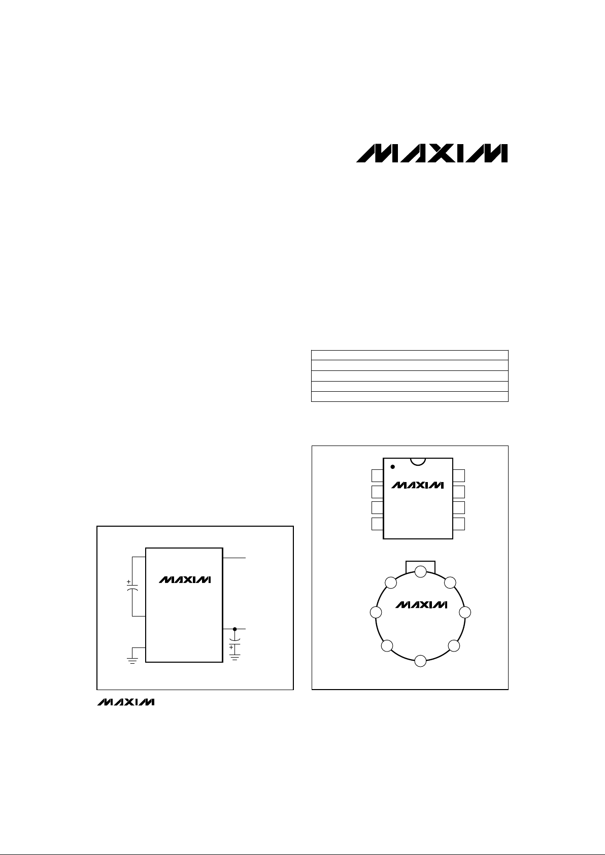
MAX1044
ICL7660
4
3
2
1
CAP-
GND
CAP+
(N.C.) BOOST
5
6
7
8
V
OUT
LV
OSC
V+
TOP VIEW
( ) ARE FOR ICL7660
DIP/SO/µMAX
TO-99
ICL7660
N.C.
CAP+
GND
CAP-
V
OUT
LV
OSC
V+ AND CASE
1
2
3
4
5
6
7
8
_________________Pin Configurations
NEGATIVE VOLTAGE CONVERTER
CAP+
CAP-
V+
V
OUT
GND
INPUT
SUPPLY
VOLTAGE
NEGATIVE
OUTPUT
VOLTAGE
MAX1044
ICL7660
__________Typical Operating Circuit
Dice*
8 SO
8 Plastic DIP
PIN-PACKAGETEMP. RANGE
0°C to +70°C
0°C to +70°C
0°C to +70°CMAX1044C/D
MAX1044CSA
MAX1044CPA
PART
8 Plastic DIP-40°C to +85°CMAX1044EPA

MAX1044/ICL7660
Switched-Capacitor Voltage Converters
2 _______________________________________________________________________________________
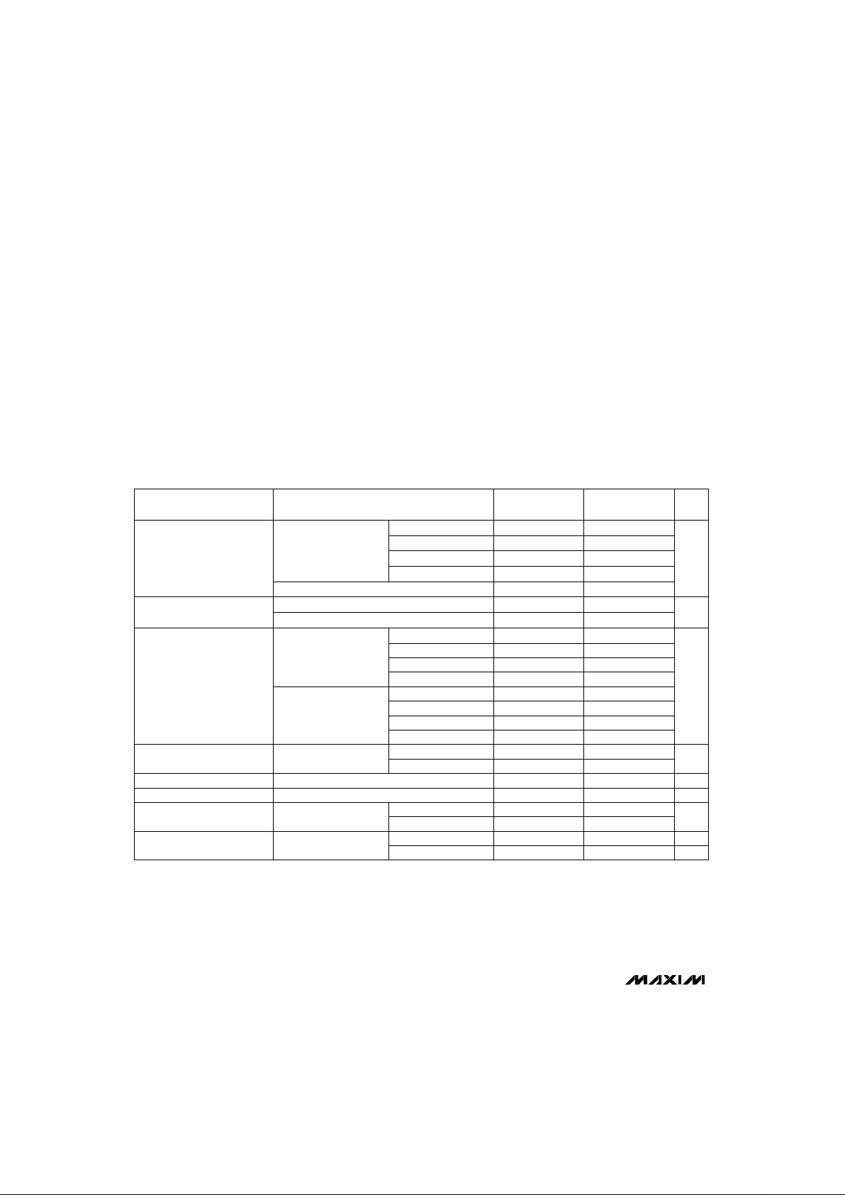
ABSOLUTE MAXIMUM RATINGS
ELECTRICAL CHARACTERISTICS
(Circuit of Figure 1, V+ = 5.0V, LV pin = 0V, BOOST pin = open, I
LOAD
= 0mA, TA= T
MIN
to T
MAX
, unless otherwise noted.)
Stresses beyond those listed under “Absolute Maximum Ratings” may cause permanent damage to the device. These are stress ratings only, and functional
operation of the device at these or any other conditions beyond those indicated in the operational sections of the specifications is not implied. Exposure to
absolute maximum rating conditions for extended periods may affect device reliability.
Note 1: The Maxim ICL7660 and MAX1044 can operate without an external output diode over the full temperature and voltage
ranges. The Maxim ICL7660 can also be used with an external output diode in series with pin 5 (cathode at V
OUT
) when
replacing the Intersil ICL7660. Tests are performed without diode in circuit.
Note 2: f
OSC
is tested with C
OSC
= 100pF to minimize the effects of test fixture capacitance loading. The 1pF frequency is correlated to this 100pF test point, and is intended to simulate pin 7’s capacitance when the device is plugged into a test socket
with no external capacitor. For this test, the LV pin is connected to GND for comparison to the original manufacturer’s
device, which automatically connects this pin to GND for (V+ > 3V).
Supply Voltage (V+ to GND, or GND to V
OUT
)....................10.5V
Input Voltage on Pins 1, 6, and 7.........-0.3V ≤ V
IN
≤ (V+ + 0.3V)
LV Input Current ..................................................................20µA
Output Short-Circuit Duration (V+ ≤ 5.5V)..................Continuous
Continuous Power Dissipation (T
A
= +70°C)
Plastic DIP (derate 9.09mW/°C above +70°C) ............727mW
SO (derate 5.88mW/°C above +70°C).........................471mW
µMAX (derate 4.1mW/°C above +70°C) ......................330mW
CERDIP (derate 8.00mW/°C above +70°C).................640mW
TO-99 (derate 6.67mW/°C above +70°C)....................533mW
Operating Temperature Ranges
MAX1044C_ _ /ICL7660C_ _ ..............................0°C to +70°C
MAX1044E_ _ /ICL7660E_ _............................-40°C to +85°C
MAX1044M_ _ /ICL7660M_ _ ........................-55°C to +125°C
Storage Temperature Range............................-65°C to + 150°C
Lead Temperature (soldering, 10sec).............................+300°C
kHz
TA= 0°C to +70°C
TA= +25°C
TA= -55°C to +125°C
V
OSC
= 0V or V+, LV open
RL= 5kΩ, TA= +25°C, f
OSC
5kHz, LV open
TA= -40°C to +85°C
RL= 10kΩ, LV open
RL= 10kΩ, LV to GND
f
OSC
= 2.7kHz (ICL7660),
f
OSC
= 1kHz (MAX1044),
V+ = 2V, IL = 3mA,
LV to GND
30 200
RL= ∞,
pins 1 and 7
no connection,
LV open
µA
10
Supply Current
20
Pin 1 = 0V
Pin 1 = V+
3
Oscillator Sink or
Source Current
%95 98Power Efficiency
C
OSC
= 1pF,
LV to GND (Note 2)
400
1
Ω
325
Output Resistance
IL= 20mA,
f
OSC
= 5kHz,
LV open
200
TA= 0°C to +70°C
TA= -40°C to +85°C
200
UNITS
MAX1044
MIN TYP MAX
PARAMETER
325
TA= +25°C
130
325
130
150
200
V
1.5 10
Supply Voltage
Range (Note 1)
65 100
5
Oscillator Frequency
100
V+ = 2V
V+ = 5V
MΩ1.0
Oscillator Impedance
80 175
95 98
400
300
250
225
ICL7660
MIN TYP MAX
300
140
250
120
150
250
3.0 10.0
1.5 3.5
55 100
10
100
1.0
TA= -55°C to +125°C
RL= ∞, pins 1 and 7 = V+ = 3V
TA= +25°C
TA= +25°C
TA= 0°C to +70°C
TA= -40°C to +85°C
TA= -55°C to +125°C
V+ = 5V
V+ = 2V
RL= ∞, TA = +25°C, LV open 99.0 99.9 %97.0 99.9Voltage Conversion Efficiency
µA
kΩ
CONDITIONS

80
90
100
30
10
1
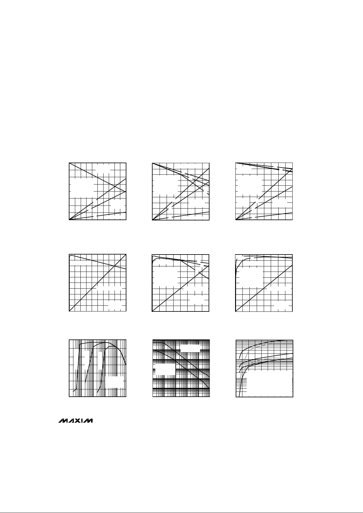
EFFICIENCY
vs. OSCILLATOR FREQUENCY
70
MAX1044-Fig 7
OSCILLATOR FREQUENCY (Hz)
EFFICIENCY (%)
10
4
50
40
10
2103
6x10
5
60
10
5
C1, C2 = 100µF
C1, C2 = 10µF
C1, C2 = 1µF
EXTERNAL
HCMOS
OSCILLATOR
10,000
100,000
0.1
1
OSCILLATOR FREQUENCY
vs. EXTERNAL CAPACITANCE
1000
MAX1044-Fig 8
C
OSC
(pF)
OSCILLATOR FREQUENCY (Hz)
1000
10
1
10 100 100,000
100
10,000
ICL7660 and
MAX1044 with
BOOST = OPEN
MAX1044 with
BOOST -V+
100
1
OSCILLATOR FREQUENCY
vs. SUPPLY VOLTAGE
MAX1044-Fig 9
SUPPLY VOLTAGE (V)
OSCILLATOR FREQUENCY (Hz)
4
10,000
1000
23 678910
100,000
5
FROM TOP TO BOTTOM AT 5V
MAX1044, BOOST = V+, LV = GND
MAX1044, BOOST = V+, LV = OPEN
ICL7660, LV = GND
ICL7660, LV = OPEN
MAX1044, BOOST = OPEN, LV = GND
MAX1044, BOOST = OPEN, LV = OPEN
0
012345678910
OUTPUT VOLTAGE and OUTPUT RIPPLE
vs. LOAD CURRENT
-0.5
-2.0
MAX1044-Fig 1
LOAD CURRENT (mA)
OUTPUT VOLTAGE (V)
OUTPUT RIPPLE (mVp-p)
-1.5
-1.0
0
250
200
150
100
50
400
350
300
OUTPUT
VOLTAGE
V+ = 2V
LV = GND
OUTPUT RIPPLE
A: MAX1044 with
BOOST = V+
B: ICL7660
C: MAX1044 with
BOOST = OPEN
A
B
C
0
0 5 10 15 20 25 30 35 40
OUTPUT VOLTAGE and OUTPUT RIPPLE
vs. LOAD CURRENT
-0.5
-2.0
-2.5
-3.0
-3.5
-4.0
-4.5
-5.0
MAX1044-Fig 2
LOAD CURRENT (mA)
OUTPUT VOLTAGE (V)
OUTPUT RIPPLE (mVp-p)
-1.5
-1.0
0
720
640
560
480
400
320
240
160
80
800
OUTPUT VOLTAGE
OUTPUT RIPPLE
V+ = 5V
LV = OPEN
A
A
B
C
B
C
A: MAX1044 with
BOOST = V+
B: ICL7660
C: MAX1044 with
BOOST = OPEN
0
0 5 10 15 20 25 30 35 40
OUTPUT VOLTAGE and OUTPUT RIPPLE
vs. LOAD CURRENT
-1
-4
-5
-6
-7
-8
-9
-10
MAX1044-Fig 3
LOAD CURRENT (mA)
OUTPUT VOLTAGE (V)
OUTPUT RIPPLE (mVp-p)
-3
-2
0
700
630
560
490
420
350
280
210
140
70
V+ = 10V
LV = OPEN
OUTPUT
RIPPLE
A
B
A: MAX1044 with
BOOST = V+
B: ICL7660
C: MAX1044 with
BOOST = OPEN
C
B
C
A
OUTPUT
VOLTAGE
0
012345678910
EFFICIENCY and SUPPLY CURRENT
vs. LOAD CURRENT
10
40
50
60
70
80
90
100
MAX1044-Fig 4
LOAD CURRENT (mA)
EFFICIENCY (%)
SUPPLY CURRENT (mA)
30
20
0
7
8
9
10
6
5
4
3
2
1
SUPPLY CURRENT
EFFICIENCY
V+ = 2V
LV = GND
0
0 5 10 15 20 25 30 35 40
EFFICIENCY and SUPPLY CURRENT
vs. LOAD CURRENT
10
40
50
60
70
80
90
100
MAX1044-Fig 5
LOAD CURRENT (mA)
EFFICIENCY (%)
SUPPLY CURRENT (mA)
30
20
0
35
40
45
50
30
25
20
15
10
5
V+ = 5V
LV = OPEN
EFFICIENCY
A: MAX1044 with
BOOST = V+
B: ICL7660
C: MAX1044 with
BOOST = OPEN
SUPPLY CURRENT
B
C
A
0
0 5 10 15 20 25 30 35 40
EFFICIENCY and SUPPLY CURRENT
vs. LOAD CURRENT
10
40
50
60
70
80
90
100
MAX1044-Fig 6
LOAD CURRENT (mA)
EFFICIENCY (%)
SUPPLY CURRENT (mA)
30
20
0
35
40
45
50
30
25
20
15
10
5
V+ = 10V
LV = OPEN
A: MAX1044 with
BOOST = V+
B: ICL7660
C: MAX1044 with
BOOST = OPEN
SUPPLY CURRENT
B, C
EFFICIENCY
A
MAX1044/ICL7660
Switched-Capacitor Voltage Converters
_______________________________________________________________________________________
3
__________________________________________Typical Operating Characteristics
(V+ = 5V; C
BYPASS
= 0.1µF; C1 = C2 = 10µF; LV = open; OSC = open; TA= +25°C; unless otherwise noted.)

0.1
12345678910
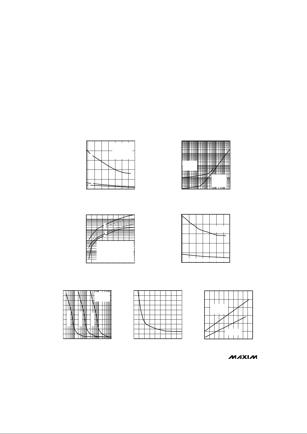
QUIESCENT CURRENT
vs. SUPPLY VOLTAGE
MAX1044-Fig 12
SUPPLY VOLTAGE (V)
QUIESCENT CURRENT (µA)
10
1
100
1000
2000
A
B
D
C
A: MAX1044, BOOST = V+, LV = GND
B: MAX1044, BOOST = V+, LV = OPEN
C: ICL7660 and MAX1044 with
BOOST = OPEN, LV = GND;
ABOVE 5V, MAX1044 ONLY
D: ICL7660 and MAX1044 with
BOOST = OPEN, LV = OPEN
0
10
1
10210310410
5
OUTPUT RESISTANCE
vs. OSCILLATOR FREQUENCY
MAX1044-Fig 14
FREQUENCY (Hz)
RESISTANCE (Ω)
200
100
300
400
500
600
700
800
900
1000
C1, C2 = 100µF
C1, C2 = 1µF
C1, C2 = 10µF
EXTERNAL
HCMOS
OSCILLATOR
0
-50 -25 0 25 50 75 100 125
QUIESCENT CURRENT
vs. TEMPERATURE
MAX1044-Fig 13
TEMPERATURE (°C)
QUIESCENT CURRENT (µA)
200
100
300
400
500
ICL7660, MAX1044 with BOOST = OPEN
MAX1044 with
BOOST = V+
0
12345678910
OUTPUT RESISTANCE
vs. SUPPLY VOLTAGE
MAX1044-Fig 15
SUPPLY VOLTAGE (V)
OUTPUT RESISTANCE (Ω)
40
20
60
80
100
120
140
160
180
200
20
-60 -40 -20 0 20 40 60 80 100 120 140
OUTPUT RESISTANCE
vs. TEMPERATURE
MAX1044-Fig 16
TEMPERATURE (°C)
OUTPUT RESISTANCE (Ω)
40
30
50
60
70
80
ICL7660,
MAX1044 with
BOOST = OPEN
MAX1044 with
BOOST = V+
MAX1044/ICL7660
Switched-Capacitor Voltage Converters
4 _______________________________________________________________________________________
____________________________Typical Operating Characteristics (continued)
(V+ = 5V; C
BYPASS
= 0.1µF; C1 = C2 = 10µF; LV = open; OSC = open; TA= +25°C; unless otherwise noted.)
0
-50
OSCILLATOR FREQUENCY
vs. TEMPERATURE
MAX1044-Fig 10
TEMPERATURE (°C)
OSCILLATOR FREQUENCY (kHz)
25
40
20
-25 0 75 100 125
60
80
100
50
A: MAX1044 with
BOOST = V+
B: ICL7600
C: MAX1044 with
BOOST = OPEN
B
A
C
1
10
0101102103104105
5x10
5
QUIESCENT CURRENT
vs. OSCILLATOR FREQUENCY
MAX1044-Fig 11
OSCILLATOR FREQUENCY (Hz)
QUIESCENT CURRENT (µA)
100
10
1000
10,000
USING
EXTERNAL
HCMOS
OSCILLATOR
USING
EXTERNAL
CAPACITOR
 Loading...