

General Description
The MAX104/MAX106/MAX108 evaluation kits (EV kits)
are designed to simplify evaluation of the devices’ analog-to-digital converters (ADCs). Each EV kit contains
all circuitry necessary to evaluate the dynamic performance of these ultra-high-speed converters, including
the power-supply generation for the PECL termination
voltage (PECLVTT). Since the design combines highspeed analog and digital circuitry, the board layout
calls for special precautions and design features.
Connectors for the power supplies (VCCA/VCCI, VCCD,
VCCO, VEE), SMA connectors for analog and clock
inputs (VIN+, VIN-, CLK+, CLK-), and all digital PECL
outputs simplify connection to the EV kit. The four-layer
board layout (GETek™ material) is optimized for best
dynamic performance of the MAX104 family.
The EV kits come with a MAX104/MAX106/MAX108
installed on the board with a heatsink attached for operation over the full commercial temperature range.
Features
♦ 50Ω Clock and Analog Inputs Through SMA
Coaxial Connectors
♦ ±250mV Input Signal Range
♦ Demultiplexed Differential PECL Outputs
♦ On-Board Generation of PECL Termination
Voltage (PECLV
TT
)
♦ On-Board Generation of ECL Termination Voltage
(ECLV
TT
)
♦ Separate Analog and Digital Power and Ground
Connections with Optimized Four-Layer PCB
♦ Square-Pin Headers for Easy Connection of Logic
Analyzer to Digital Outputs
♦ Fully Assembled and Tested
Evaluate: MAX104/MAX106/MAX108
MAX104/MAX106/MAX108 Evaluation Kits
________________________________________________________________
Maxim Integrated Products
1
19-1503; Rev 0; 6/99
Component List
PART
MAX104EVKIT
MAX106EVKIT
0°C to +70°C
0°C to +70°C
TEMP.
RANGE
PIN-
PACKAGE
192 ESBGA
192 ESBGA
For free samples & the latest literature: http://www.maxim-ic.com, or phone 1-800-998-8800.
For small orders, phone 1-800-835-8769.
Ordering Information
Not populated; see text for description of reset input operation.
2R3, R4
DESIGNATION
10kΩ potentiometer 1R2
1N5819 Schottky diode1D1
47pF ±10% ceramic capacitors
(0402)
20
C3–C6, C15, C16,
C22–C25,
C33–C37,
C42–C45, C50
0.01µF ±10% ceramic capacitors
(0603)
30
C2, C7–C12, C14,
C17, C18, C19,
C21, C26–C30,
C32, C41, C47,
C49, C51–C59
10µF ±10%, 16V tantalum caps
AVX TAJD106D016
7
C1, C13, C20, C31,
C40, C46, C48
DESCRIPTIONQTY
MAX108EVKIT*
0°C to +70°C 192 ESBGA
SAMPLING
RATE
1Gsps
600Msps
1.5Gsps
GETek is trademark of GE Electromaterials.
49.9Ω ±1% resistors (0603)38
R5–R38,
R44–R47
DESIGNATION DESCRIPTIONQTY
2-pin headers41
JU2, JU4, JU5,
JUA0- to JUA7-,
JUA0+ to JUA7+,
JUP0- to JUP7-,
JUP0+ to JUP7+,
JUOR+, JUOR-,
JUDR-, JUDR+,
JURO-, JURO+
3-pin headers5JU3, JU6–JU9
SMA connectors (edge mounted)10J1–J10
158Ω ±1% resistors (0603)2R52, R54
243Ω ±1% resistors (0603)2R51, R53
*
Future product—contact factory for availability.
查询MAX104EVKIT供应商

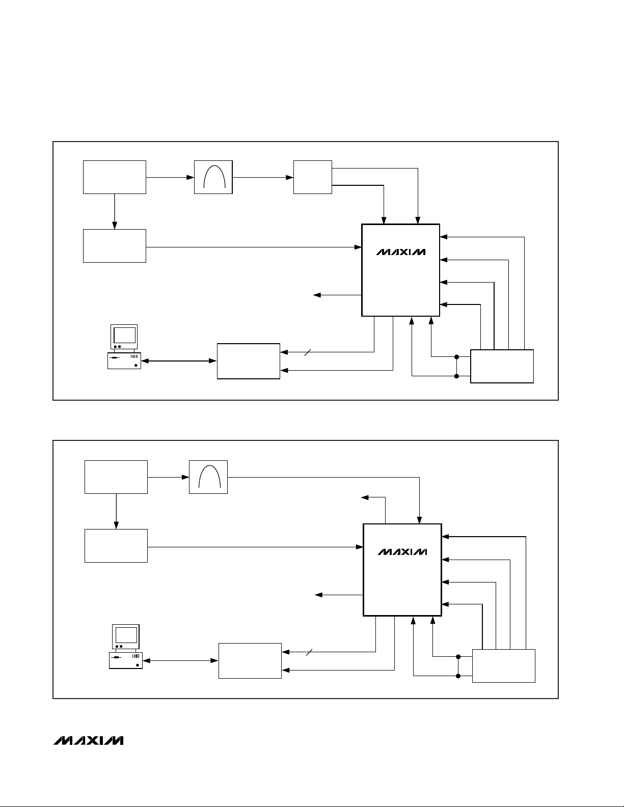
_________________________Quick Start
The EV kit is delivered fully assembled, tested, and
sealed in an antistatic bag. To ensure proper operation,
open the antistatic bag only at a static-safe work area
and follow the instructions below. Do not turn on the
power supplies until all power connections to the
EV kit are established. Figure 1 shows a typical evalu-
ation setup with differential analog inputs and singleended sine- wave (CLK- is 50Ω reverse-terminated to
GNDI) clock drive. Figure 2 shows a typical evaluation
setup with single-ended analog inputs (VIN- is 50Ω
reverse-terminated to GNDI) and a single-ended sinewave clock drive.
1) Connect a -5V power supply capable of providing
-250mA to the pad marked VEE. Connect the supply’s ground to the GNDI pad. Set the current limit
to 500mA or less.
2) Connect a +5V power supply capable of providing
600mA to the VCCI pad. Connect the supply’s
ground to the GNDI pad.
3) Connect a +5V power supply capable of providing
250mA to the VCCD pad. Connect the supply’s
ground to the GNDD pad.
4) Connect a +3.3V or +5V power supply capable of
providing approximately 600mA to the VCCO pad.
Connect the supply’s ground to the GNDD pad.
5) Connect GNDI to GNDD at the power supplies.
6) Connect an RF source with low phase jitter, such as
an HP8662A (up to 1.28GHz) or an HP8663A (up to
2.56GHz), to clock inputs CLK- and CLK+. For single-ended clock inputs, feed a +4dBm (500mV
amplitude) power level from the signal generator
into the CLK+ input and terminate the unused CLKinput with 50Ω to GNDI.
7) Connect a ±225mV (approximately -1dB below FS)
sine-wave test signal to the analog inputs. Use
VIN+ and VIN- through a balun if the test signal is
differential, or either VIN+ or VIN- if the signal is single-ended (see the sections
Single-Ended Analog
Inputs
and
Differential Analog Inputs
in the devices’
data sheets). For best results, use a narrow bandpass filter designed for the frequency of interest to
reduce the harmonic distortion from the signal generator.
8) Connect a logic analyzer, such as an HP16500C
with an HP16517A plug-in card for monitoring all 16
output channels (8 channels for primary and 8
channels for auxiliary outputs) of the device.
9) Connect the logic analyzer clock to the DREADY+
output on the EV kit, and set the logic analyzer to
trigger on the falling edge of the acquisition clock.
Set the logic analyzer’s threshold voltage to the
VCCO supply voltage -1.3V. For example, if VCCO =
+3.3V, the threshold voltage should be set to
+2.0V.
10) Turn on the supplies and signal sources. Capture
the digitized outputs from the ADC with the logic
analyzer and transfer the digital record to a PC for
data analysis.
Evaluate: MAX104/MAX106/MAX108
MAX104/MAX106/MAX108 Evaluation Kits
2 _______________________________________________________________________________________
Component List (continued)
Shunts7None
Test points24
VCCO, VCCD,
GNDD, PECLVTT,
GNDA, VCCA,
VCCI, GNDI, VEE,
ECLV
TT
Protective feet4None
Heatsink
International Electronic Research
Corp. BDN09-3CB/A01
1None
MAX104CHC, MAX106CHC, or
MAX108CHC (192-contact ESBGA™)
1U1
LM2991S, low-dropout adjustable
linear regulator
2U3, U4
MAX104EVKIT circuit board1None
MAX104, MAX106, or MAX108 data
sheet
1None
DESIGNATION DESCRIPTIONQTY
ESBGA is a trademark of Amkor/Anam.
Evaluate: MAX104/MAX106/MAX108
MAX104/MAX106/MAX108 Evaluation Kits
_______________________________________________________________________________________ 3
MAX104
MAX106
MAX108
EV KIT
BALUN
HP8662/3A
SINE-WAVE SOURCE
PHASE
LOCKED
f
SAMPLE
, + 4dBm
EXTERNAL 50Ω
TERMINATION TO GNDI
HP8662/3A
SINE-WAVE SOURCE
POWER
SUPPLIES
GNDD
+5V ANALOG
VIN+VIN-
CLK+
CLK-
16 DATA
DREADY+
-5V ANALOG
+5V DIGITAL
+3.3V DIGITAL
GNDI
HP16500C
DATA ANALYSIS
SYSTEM
GPIB
PC
BPF
Figure 1. Typical Evaluation Setup with Differential Analog Inputs and Single-Ended Clock Drive
MAX104
MAX106
MAX108
EV KIT
HP8662/3A
SINE-WAVE SOURCE
PHASE
LOCKED
f
SAMPLE
, + 4dBm
EXTERNAL 50Ω
TERMINATION TO GNDI
EXTERNAL 50Ω
TERMINATION
TO GNDI
HP8662/3A
SINE-WAVE SOURCE
POWER
SUPPLIES
GNDD
+5V ANALOG
VIN+VIN-
CLK+
CLK-
16 DATA
DREADY+
-5V ANALOG
+5V DIGITAL
+3.3V DIGITAL
GNDI
HP16500C
DATA ANALYSIS
SYSTEM
GPIB
PC
BPF
Figure 2. Typical Evaluation Setup with Single-Ended Analog Inputs and Single-Ended Clock Drive

Evaluate: MAX104/MAX106/MAX108
MAX104/MAX106/MAX108 Evaluation Kits
4 _______________________________________________________________________________________
_______________Detailed Description
Clock Input Requirements
The MAX104/MAX106/MAX108 feature clock inputs
designed for either single-ended or differential operation with very flexible input drive requirements. Each
clock input is terminated with an on-chip, laser-trimmed
50Ω resistor to CLKCOM (clock termination return). The
traces from the SMA inputs to the high-speed data converter are 50Ω microstrip transmission lines.
The CLKCOM termination voltage may be connected
anywhere between ground and -2V for compatibility
with standard ECL drive levels. The side-launched SMA
connectors for the clock signals are located at the
lower left corner of the EV board and are labeled J3
(CLK+) and J4 (CLK-).
An on-board bias generator, located between the analog and clock inputs, creates a -2V termination voltage
(ECLVTT) for operation with ECL clock sources. The
voltage is generated by an LM2991 voltage regulator
operated from the board’s -5V VEEpower supply. To
enable this ECLVTTbias generator, first remove shorting jumper JU2, then move jumper JU3 into its ON
position.
The voltage regulator has a shutdown control that
requires a TTL logic-high level to enter the shutdown
state. This logic level is derived from the +5V analog
supply (VCCI). The EV kits are delivered with the
ECLVTTbias generator turned off and CLKCOM tied to
GNDI (JU2 installed).
NOTE: If the regulator’s shutdown logic level is not
present (VCCI on first) before the VEEsupply is
turned on, the regulator will momentarily turn on
until the VCCI supply is energized. If JU2 is installed,
this will momentarily short the regulator’s output to
ground. The regulator is short-circuit protected so
no damage will result. The regulator is further protected by limiting the V
EE
supply current to 500mA.
Single-Ended Clock Inputs
(Sine-Wave Drive)
To obtain the lowest jitter clock drive, AC- or DC-couple
a low-phase-noise sine-wave source into a single clock
input. Clock amplitudes of up to 1V (2Vp-p or +10dBm)
can be accommodated with CLKCOM connected to
GNDI.
The dynamic performance of the data converter is
essentially unaffected by clock-drive power levels from
-10dBm to +10dBm (100mV to 1V clock signal ampli-
tude). The dynamic performance specifications are
measured with a single-ended clock drive of +4dBm
(500mV clock signal amplitude). To avoid saturation of
the input amplifier stage, limit the clock power level to a
maximum of +10dBm.
Differential Clock Inputs (ECL Drive)
The MAX104/MAX106/MAX108 clock inputs may also
be driven with standard ground-referenced ECL logic
levels by using the on-board ECLVTT-2V bias generator as described above. It is also possible to drive the
clock inputs with positive supply referenced (PECL)
levels if the clock inputs are AC-coupled. With AC-coupled clock inputs, the CLKCOM termination voltage
should be grounded. Single-ended DC-coupled ECL
drive is possible as well, if the undriven clock input is
tied to the ECL VBBvoltage (-1.3V nominal).
Analog Input Requirements
The analog inputs to the ADC on the EV board are provided by two side-launch SMA connectors located on
the middle left side of the EV kit. They are labeled J1
(VIN+) and J2 (VIN-). The analog inputs are terminated
on-chip with precision laser-trimmed 50Ω NiCr resistors
to GNDI. Although the analog (and clock) inputs are
ESD protected, good ESD practices should always be
observed. The traces from the SMA inputs to the device
are 50Ω microstrip transmission lines. The analog
inputs can be driven either single-ended or differential.
Optimal performance is obtained with differential input
drive due to reduction of even-order harmonic distortion. Table 1 represents single-ended input drive, and
Table 2 displays differential input drive.
Table 1. Input Setup and Output Code Results for Single-Ended Analog Inputs
0V+250mV - 1LSB
0V+250mV
VIN+ VIN-
0
1
OVERRANGE BIT
11111111
11111111 (full scale)
OUTPUT CODE
00V-250mV + 1LSB
0
00000001
01111111
toggles 10000000
0V0V
00V-250mV 00000000 (zero scale)
Evaluate: MAX104/MAX106/MAX108
MAX104/MAX106/MAX108 Evaluation Kits
_______________________________________________________________________________________ 5
Internal Reference
The MAX104 family features an on-chip +2.5V precision
bandgap reference, which can be used by shorting
jumper JU5 to connect REFOUT with REFIN. If
required, REFOUT can also source up to 2.5mA to supply other peripheral circuitry.
To use an external reference, remove the shorting
jumper on JU5 and connect the new reference voltage
source to the REFIN side of JU5. Leave the REFOUT
side of JU5 floating. Connect the ground of the external
reference to GNDI on the EV kit. REFIN accepts an
input voltage range of +2.3V to +2.7V.
CAUTION: With an external reference connected,
JU5 must not be installed at any time to avoid damaging the internal reference with the external reference supply.
Offset Adjust
The devices also provide a control input (VOSADJ) to
eliminate any offset from additional preamplifiers driving the ADC. The VOSADJ control input is a selfbiased voltage divider from the internal +2.5V precision
reference. Under normal-use conditions, the control
input is left floating.
The EV kits include a 10kΩ potentiometer that is biased
from the ADC’s +2.5V reference. The wiper of the
potentiometer connects to the VOSADJ control input
through JU4. To enable the offset-adjust function, install
a shorting jumper on JU4 and adjust potentiometer R2
while observing the resulting offset in the reconstructed
digital outputs. The offset-adjust potentiometer offers
about ±5.5LSB of adjustment range. The EV kits are
shipped from the factory without a shorting jumper
installed on JU4.
Primary and Auxiliary
PECL Outputs
All PECL outputs on the EV kits are powered from the
VCCO power supply, which may be operated from any
voltage between +3.0V to +5.0V for flexible interfacing
with either +3.3V or +5V systems. The nominal VCCO
supply voltage is +3.3V.
The PECL outputs are standard open-emitter types and
require external 50Ω termination resistors to the
PECLV
TT
voltage for proper biasing. The termination
resistors are located at the far end of each 50Ω
microstrip transmission line, very close to the square
pin headers for the logic analyzer interface. Every EV
board is delivered with the PECL termination resistors
installed on the back side of the board. Each output
links to a 0.100 inch square 2-pin header to ease the
connection to a high-speed logic analyzer such as
Hewlett Packard’s HP16500C.
To capture the digital data from the device in demultiplexed 1:2 format, each of the 16 channels from the
logic analyzer is connected to the eight primary (P0 to
P7) and eight auxiliary (A0 to A7) outputs. The ADC
provides differential PECL outputs, but most logic analyzers (such as the HP16500C) have single-ended
acquisition pods. Connect all single-ended logic analyzer pods to the same phase (either “+” or “-”) of the
PECL outputs.
Data Ready (DREADY) Output
The clock pod from the logic analyzer should be connected to the DREADY+ output at JUDR+ on the EV
kits. Since both the primary and auxiliary outputs
change on the rising edge of DREADY+, set the logic
analyzer to trigger on the falling edge. The DREADY
and data outputs are internally time-aligned, which
places the falling edge of DREADY+ in the approximate
center of the valid data window, resulting in the maximum setup and hold time for the logic analyzer. Set the
logic analyzer’s threshold voltage to VCCO - 1.3V. For
example, if VCCO is +3.3V, the threshold voltage
should be set to +2.0V. The sample offset (trigger
delay) of the logic analyzer should be set to 0ps under
these conditions.
It is also possible to use the DREADY- output for the
acquisition clock. Under this condition, set the logic
analyzer to trigger on the rising edge of the clock.
Table 3 summarizes the digital outputs and their functions.
Table 2. Input Setup and Output Code Results for Differential Analog Inputs
0-125mV + 0.5LSB+125mV - 0.5LSB
1
OVERRANGE BIT
11111111
11111111 (full scale)-125mV+125mV
OUTPUT CODE
0+125mV - 0.5LSB-125mV + 0.5LSB
0
00000001
01111111
toggles 10000000
0V0V
0+125mV-125mV 00000000 (zero scale)
VIN+ VIN-

Evaluate: MAX104/MAX106/MAX108
MAX104/MAX106/MAX108 Evaluation Kits
6 _______________________________________________________________________________________
Demultiplexer Settings
Demultiplexed DIV2 Mode
This mode reduces the output data rate to one-half the
sample clock rate. The demultiplexed outputs are presented in dual 8-bit format with two consecutive samples in the primary and auxiliary output ports on the rising edge of the data ready clock. To activate this
mode, jumpers JU7 (DEMUXEN), JU8 (AUXEN2), and
JU9 (AUXEN1) have to be in the ON position, and
DIVSELECT (JU6) must be set to position 2.
NOTE: Each EV kit is shipped with jumpers JU7,
JU8, and JU9 installed in the ON position and JU6
set to 2.
Non-Demultiplexed DIV1 Mode
It is also possible to operate the ADC in a non-demultiplexed mode. In this mode, the internal demultiplexer is
disabled and the sampled data is presented to the primary output port only. To consume less power, the auxiliary port can be shut down by two separate inputs
(AUXEN1 and AUXEN2). To enter this mode, place
jumpers JU7 (DEMUXEN), JU8 (AUXEN2), and JU9
(AUXEN1) in the OFF position. The position of the DIVSELECT (JU6) jumper is a don’t care. To save additional
power, remove all the 50Ω pull-down resistors (R5–R20)
on the auxiliary output port. It is not necessary to
remove the resistors; however, both the true and complementary PECL outputs will pull up to the VOHlevel.
Table 3. PECL Outputs and Functions
JUA0+ to JUA7+,
JUA0- to JUA7-
A0+ to A7+,
A0- to A7-
JUP0+ to JUP7+,
JUP0- to JUP7-
P0+ to P7+,
P0- to P7-
JUOR+, JUOR-OR+, ORJUDR+, JUDR-DREADY+, DREADY-
PECL OUTPUT
SIGNALS
EV KIT JUMPER
LOCATION
Auxiliary Port Differential Outputs from LSB to
MSB. A “+” indicates the true value; a “-”
denotes the complementary outputs.
Primary Port Differential Outputs from LSB to
MSB. A “+” indicates the true value; a “-”
denotes the complementary outputs.
Overrange’s True and Complementary Outputs.
Data-Ready PECL Output Latch Clock. Output
data changes on the rising edge of DREADY+.
FUNCTION
Demux Reset Input Signals. Resets the internal
demux when asserted.
Reset Outputs—for resetting additional external
demux devices.
J5, J6 (SMA connectors)RSTIN+, RSTIN-
JURO+, JURO-RSTOUT+, RSTOUT-
DEMUXEN (JU7)
•
OFF ON
AUXEN2 (JU8)
•
OFF ON
AUXEN1 (JU9)
•
OFF ON
DIVSELECT (JU6)
•
24
•
•
•
•
DEMUXEN (JU7)
•
OFF ON
AUXEN2 (JU8)
•
OFF ON
AUXEN1 (JU9)
•
OFF ON
DIVSELECT (JU6)
X
2
X = Leave open or don’t care
•
•
•
X
X
4

Evaluate: MAX104/MAX106/MAX108
MAX104/MAX106/MAX108 Evaluation Kits
_______________________________________________________________________________________ 7
Decimation DIV4 Mode
In this special decimated, demultiplexed output mode,
the ADC discards every other input sample and outputs
data at one-quarter the input sampling rate. This mode
is useful for system debugging at the resulting slower
output data rates, and may be required to capture data
successfully when testing the MAX108. To activate the
EV board’s DIV4 mode, jumpers JU7 (DEMUXEN), JU8
(AUXEN2), and JU9 (AUXEN1) have to be in the ON
position, and DIVSEL has to be in position 4. Since
every other sample at the input is discarded, the converter’s effective sample rate will be f
SAMPLE
/2.
Overrange Operation
A single differential PECL overrange output bit (OR+,
OR-) is provided for both primary and auxiliary demultiplexed outputs. The operation of the overrange bit
depends on the status of the internal demultiplexer. In
demultiplexed DIV2 mode and decimation DIV4 mode,
the OR bit will flag an overrange condition if either the
primary or auxiliary port contains an overranged sample (Table 4). In non-demultiplexed DIV1 mode, the OR
port will flag an overrange condition only when the primary output port contains an overranged sample.
Reset Operation Requirements
A detailed description of the reset circuitry and its operation is located in each device’s data sheet. To use the
reset input function, install two 50Ω pull-down resistors
at positions R3 and R4 on the back side of the EV
board. These resistors are connected to the on-board
PECLVTTtermination generator. The RSTIN logic levels
are compatible with standard PECL levels referenced
from the VCCO power supply.
The signals associated with the demultiplexer reset
operation and the control of this section are listed in
Table 5. Consult the data sheet for a more detailed
description of the demultiplexer reset function, including timing diagrams.
Reset Inputs
The reset circuitry accepts differential PECL inputs referenced to the same VCCO power supply that powers
the ADC’s PECL outputs. The reset input side-launched
SMA connectors are located at the lower left side of the
EV kits and are labeled RSTIN+ and RSTIN-.
For applications that do not require a synchronizing
reset, the reset inputs must be left open and resistors
R3 and R4 removed. In this case, they will self-bias to a
proper level with internal 50kΩ resistors and a 20µA
current source. This combination creates a -1V voltage
difference between RSTIN+ and RSTIN- to disable the
internal reset circuitry. When driven with PECL logic
levels terminated with 50Ω to VCCO - 2V, the internal
biasing network can easily be overdriven. The EV kits
are shipped with these resistor positions open to allow
the internal self-bias circuitry to disable the reset control input.
NOTE: Do not install the 50Ω RSTIN termination
resistors R3 and R4 unless the RSTIN input is driven with valid PECL logic levels. If the RSTIN inputs
are open circuited with the 50Ω resistors installed,
intermittent resetting of the internal demultiplexer
will occur and unpredictable operation will result.
Table 4. Selection Table for
Demultiplexer Operation
DIV22ON
DIV1
DEMUX
MODE
Primary OR auxiliary
port
Only primary port
active (auxiliary port
off)
XOFF
OVERRANGE BIT
OUTPUT MODE
DIV44ON
Primary OR auxiliary
port
DEMUXEN DIVSELECT
X = Don’t care
DEMUXEN
OFF ON
•
•
AUXEN2
OFF ON
•
•
AUXEN1
OFF ON
•
•
DIVSELECT
24
•
•

Evaluate: MAX104/MAX106/MAX108
MAX104/MAX106/MAX108 Evaluation Kits
8 _______________________________________________________________________________________
Reset Outputs
With a single device, no synchronizing reset is required
since the order of the samples in the output ports is
unchanged regardless of the phase of the DREADY
(DREADY+, DREADY-) clock (as described in the data
sheets). DREADY+ (jumper JUDR+) and DREADY(jumper JUDR-) can be found in the middle of the PECL
output arc in the right center of the EV board.
On the EV kits, the reset output 2-pin headers for
RSTOUT+ (jumper JURO+) and RSTOUT- (jumper
JURO-) are located above the reset input SMA connectors on the lower left side of the board.
Power Supplies
The EV kits feature separate analog and digital power
supplies and grounds for best dynamic performance. The
power-supply connectors are located at the top of the
board and require the power supplies listed in Table 6.
To simplify use of the EV kits and reduce the number of
power sources required to drive the EV board, VCCA
and VCCI, as well as GNDA and GNDI, are connected
together by shorting straps SP1 and SP2. To separate
the supplies, cut the traces at SP1 and SP2. Be sure to
observe the absolute maximum voltage difference of
±0.3V between the supplies if separate supplies are
used. This may require back-to-back Schottky diodes
between VCCA and VCCI to prevent violation of the
absolute maximum ratings during power-up/down.
The EV kits are tested with the V
CC
A and VCCI supplies
shorted by SP1 and SP2. There is no measurable difference in the parts’ dynamic performance with the supplies separated, therefore Maxim recommends leaving
the supplies connected together.
CAUTION: There are no connections between
GNDA/GNDI and GNDD on the EV kits. These
grounds must be referenced together at the power
supply to the board, or damage to the device may
result!
Referencing analog (GNDA/GNDI) and digital (GNDD)
grounds together at a single point avoids ground loops
and reduces noise pickup from the digital signals or
power lines.
To avoid a possible latchup condition when disassembling an application, a high-speed Schottky diode (D1,
1N5819) was added between V
EE
and GNDI. This
diode prevents the substrate (which is connected to
VEE) from forward biasing and possibly causing a
latchup condition when the VEEconnector is opened.
Board Layout
Each EV kit is a four-layer board design, optimized for
high-speed signals. The board is constructed from lowloss GETek core material, which has a relative dielectric constant of 3.9 (εr= 3.9). The GETek material used
for the EV board offers improved high-frequency and
thermal properties over standard FR4 board material.
All high-speed signals are routed with 50Ω microstrip
Table 6. Power-Supply and Ground Requirements and Location
J11VCCD = +5V
J17VEE= -5V
J13, J15VCCA = VCCI = +5V
POWER SUPPLY
EV KIT JUMPER
LOCATION
GNDD
GNDI
GNDA/GNDI
GROUND
REFERENCE
J12
J16
J14, J16
EV KIT JUMPER
LOCATION
J18VCCO = +3.0V to +5V J12GNDD
Table 5. Demultiplexer Operation and Reset Control Signals
JURO+, JURO-
JUDR+, JUDR-DREADY+, DREADY-
RSTOUT+, RSTOUT- Reset Output—for resetting additional external demux devices.
Data-Ready PECL Output. Output data changes on the rising edge of
DREADY+.
Master ADC Timing Signal. The ADC samples on the rising edge of CLK+.J3, J4CLK+, CLK-
FUNCTION
J5, J6RSTIN+, RSTIN- Demux Reset Input Signal. Resets the internal demux when asserted.
SIGNAL NAME
EV KIT JUMPER
LOCATION

Evaluate: MAX104/MAX106/MAX108
MAX104/MAX106/MAX108 Evaluation Kits
_______________________________________________________________________________________ 9
transmission lines. The line width for 50Ω microstrip is
18 mils with a ground plane height of 10 mils, which is
a standard GETek core thickness. Figure 3 shows a
cross-section of the EV kit layer profile.
The board also features a de-embedding fixture formed
from two lengths of microstrip transmission line connected between SMA connectors J9-10 and J7-8,
located on the right edge of the board. The 1.50-inch
line length difference between the two paths exactly
matches the line length of the microstrip connecting the
analog inputs. By measuring the power-loss difference
between the two paths at the frequency of interest, it is
possible to estimate the attenuation of the analog
inputs caused by PCB losses. Figure 4 shows the measured attenuation vs. frequency for the microstrip lines
connecting the analog inputs.
Special Layout Considerations
A special effort was made in the board layout to separate the analog and digital portions of the circuit. 50Ω
microstrip transmission lines are used for the analog
and clock inputs as well as for the high-speed PECL
digital outputs. The analog and clock transmission lines
are formed on the top side of the board, while the digital transmission lines are located on the back side of
the board. This reduces coupling of the high-speed
digital outputs to the analog inputs. The analog and
clock inputs provide on-chip, laser-trimmed 50Ω termi-
nation resistors for the best VSWR performance.
Wherever large ground or power planes are used, care
was taken to ensure that the analog planes were not
overlapping with any digital planes. This eliminates the
possibility of capacitively coupling digital noise through
the circuit board to sensitive analog areas.
Table 7. EV Kit PCB Layers
LAYER #1 (TOP)
18 MILS
50Ω
1 oz. Cu
LAYER #2
18 MILS
50Ω
10 MIL GETek CORE
GETek PREPREG AS NEEDED
10 MIL GETek CORE
LAYER #3
LAYER #4 (BOTTOM)
Figure 3. EV Kit Layer Profile for 50ΩMicrostrip Design
0
-0.05
-0.10
-0.15
-0.20
-0.25
-0.30
-0.35
-0.40
-0.45
-0.50
1 500 1500 2500
BOARD LOSS vs. INPUT FREQUENCY
ANALOG INPUT FREQUENCY (MHz)
AMPLITUDE (dB)
Figure 4. Analog Input Attenuation from PCB Losses
VEE, PECLVTT(VCCO - 2V), GNDD
VCCA, VCCO, GNDI, digital 50Ω microstrip lines, 50Ω termination resistorsLayer IV, bottom layer
Layer III, power plane
Components, jumpers, connectors, test pads, VCCO, GNDD, GNDI, analog 50Ω
microstrip lines, de-embedding fixtures
Layer I, top layer
Ground for analog 50Ω microstrips, GNDA, GNDD, GNDI, VCCDLayer II, ground plane
LAYER DESCRIPTION

Evaluate: MAX104/MAX106/MAX108
All differential digital outputs are properly terminated
with 50Ω termination resistors on both phases of the
output, even though most logic analyzers are single
ended. By terminating both sides of the differential outputs, the AC current in the VCCO and GNDD supplies is
reduced. This also reduces coupling of the ADC outputs back to the analog inputs and preserves the
excellent SNR performance of the converter.
The PECL digital outputs are arranged in an arc to match
the line lengths between the ADC outputs and the logic
analyzer connectors. The lengths of the 50Ω microstrip
lines are matched to within 0.050 inch to minimize layoutdependent data skew between the bits. The propagation
delay on the EV board is about 134ps per inch.
ESBGA Device Pad Design
An excellent reference on the assembly and design of
PCBs with BGA devices is “
Application Notes on
Surface Mount Assembly of Amkor/Anam BGA
Packages
.” This publication is available from
Amkor/Anam, 1900 S. Price Road, Chandler AZ, 85248,
phone: (602) 821-5000.
As described in the above applications note, there are
two possibilities for defining PCB pads for mounting
BGA devices: solder mask defined (SMD) and nonsolder mask defined (non-SMD, copper defined). The EV
kits’ design employs nonsolder mask defined pads.
Figure 5 shows the layout of each of these pad types.
The non-SMD (Figure 5b) pad has a solder-mask opening that is larger than the copper land area. This means
that the size of the mounting pad is controlled by the
copper etch quality control. The SMD pad (Figure 5a)
has a solder-mask opening that is smaller than the copper land area. This means that the solder-mask alignment and etch quality will control the pad dimensions.
Since the edges of the copper do not need to extend
under the solder mask as with the SMD pad, the pad
can either be made larger or can provide more line
routing space between adjacent pads. There is room to
route a single 50Ω microstrip trace (18 mils wide)
between the BGA mounting pads on the EV kits. The
copper land diameter is 25 mils, while the solder mask
opening is 30 mils.
Die Temperature Measurement
It is possible to determine the die temperature of the
ADC under normal operating conditions by observing
the currents I
CONST
and I
PTAT
. These are two nominally
100µA currents designed to be equal at 27°C. The currents are derived from the internal precision +2.5V
bandgap reference of the ADC. Their test pads (J21
and J22) are labeled ICONST and IPTAT and are located just above the analog inputs.
The simplest method of determining die temperature is
to measure each current with an ammeter referenced to
GNDI, as described in the data sheets. The die temperature in °C is then calculated by the expression:
T 300
I
I
273
DIE
PTAT
CONST
=
−
⋅
MAX104/MAX106/MAX108 Evaluation Kits
10 ______________________________________________________________________________________
Figure 5a. BGA PCB Pad Designs (SMD Pad) Figure 5b. BGA PCB Pad Designs (Non-SMD Pad)

Evaluate: MAX104/MAX106/MAX108
MAX104/MAX106/MAX108 Evaluation Kits
______________________________________________________________________________________ 11
C1
10µF
C7
0.01µF
C2
0.01µF
C3
47pF
C4
47pF
C6
47pF
C5
47pF
V
CC
D
J11
J12
GNDD
C20
10µF
C21
0.01µF
C9
0.01µF
C22
47pF
C23
47pF
C25
47pF
C24
47pF
V
CC
I
J15
J16
GNDI
C13
10µF
C14
0.01µF
C8
0.01µF
C15
47pF
C16
47pF
V
CC
A
J13
GNDA
J14
C40
10µF
C41
0.01µF
C11
0.01µF
C42
47pF
C43
47pF
C45
47pF
C44
47pF
V
CC
O
J18
R53
243Ω
R54
158Ω
U4
LM2991
GND
OUT
IN
ADJ
1
2
3
5
4
J19
PECLV
TT
C46
10µF
C47
0.01µF
GNDD
SP2
SP1
V
EE
GNDD
J17
J20
GNDI
D1
C31
10µF
R51
243Ω
R52
158Ω
U3
LM2991
ADJ IN
OUT
GND
4
2
5
3
1
GNDI
3
1
2
V
CC
I
ON OFF
JU3
GNDI
C37
47pF
C32
0.01µF
C10
0.01µF
C33
47pF
C34
47pF
C35
47pF
C36
47pF
C48
10µF
C49
0.01µF
C50
47pF
ECLV
TT
ON/OFF
ON/OFF
GNDD
Figure 6. MAX104/MAX106/MAX108 EV Kits Schematic

Evaluate: MAX104/MAX106/MAX108
MAX104/MAX106/MAX108 Evaluation Kits
12 ______________________________________________________________________________________
VCCO
V
TT
GNDD
C12
0.01µF
C51
0.01µF
VCCO
V
TT
GNDD
C29
0.01µF
C58
0.01µF
VCCO
NOTE: THESE JUMPERS FORM
THE DE-EMBEDDING FIXTURE.
J7
J9
J8
J10
V
TT
GNDD
C18
0.01µF
C53
0.01µF
VCCO
V
TT
GNDD
C17
0.01µF
C52
0.01µF
EXAMPLE FOR PECL OUTPUT
JUMPER AND TERMINATION.
(EACH OUTPUT ON THE EV KIT
IS TERMINATED LIKE THIS.)
VCCO
V
TT
GNDD
GNDD
PECLV
TT
JUOR+
R28
49.9Ω
C30
0.01µF
C59
0.01µF
VCCO
V
TT
GNDD
C28
0.01µF
C57
0.01µF
VCCO
V
TT
GNDD
C27
0.01µF
C58
0.01µF
VCCO
V
TT
GNDD
C26
0.01µF
C55
0.01µF
VCCO
V
TT
GNDD
C19
0.01µF
C54
0.01µF
JUOR+
JUORJUP7+
JUP7JUP6+
JUP6JUP5+
JUP5JUP4+
JUP4JUP3+
JUP3JUP2+
JUP2JUP1+
JUP1JUP0+
JUP0JUA7+
JUA7JUA6+
JUA6JUA5+
JUA5JUA4+
JUA4JUA3+
JUA3JUA2+
JUA2JUA1+
JUA1JUA0+
JUA0JUDRJUDR+
JUROJURO+
R28
R29
R30
R38
R37
R36
R35
R34
R33
R32
R31
R27
R26
R25
R24
R23
R22
R21
R20
R19
R18
R17
R16
R15
R14
R13
R12
R11
R10
R9
R8
R7
R6
R5
R44
R45
R46
R47
JUMPER
TERMINATION
RESISTOR TO V
TT
JUOR+
Figure 6. MAX104/MAX106/MAX108 EV Kits Schematic (continued)

Evaluate: MAX104/MAX106/MAX108
MAX104/MAX106/MAX108 Evaluation Kits
______________________________________________________________________________________ 13
MAX104
MAX106
MAX108
U1
JUOR+
JUORJUP7+
JUP7JUP6+
JUP6JUP5+
JUP5JUP4+
JUP4JUP3+
JUP3JUP2+
JUP2JUP1+
JUP1JUP0+
JUP0JUA7+
JUA7JUA6+
JUA6JUA5+
JUA5JUA4+
JUA4JUA3+
JUA3JUA2+
JUA2JUA1+
JUA1JUA0+
JUA0-
JUDRJUDR+
JUROJURO+
OR+
ORP7+
P7P6+
P6P5+
P5P4+
P4P3+
P3P2+
P2P1+
P1P0+
P0A7+
A7A6+
A6A5+
A5A4+
A4A3+
A3A2+
A2A1+
A1A0+
A0-
OFF
ON
JU7
GNDD
1
2
3
VCCD
D17
E18
V12
U12
V14
U14
V16
U16
N18
N17
L18
L17
H18
H17
F18
F17
B14
C14
B12
C12
V13
U13
V15
U15
P18
P17
M18
M17
J18
J17
G18
G17
B15
C15
B13
C13
DIVSEL
DEMUXEN
24
JU5
GNDD
1
2
3
VCCD
GNDD
V11
U11
K18
K17
RSTOUT+
RSTOUT-
DREADY+
DREADY-
GNDI
P2
T.P.
VOSADJ
ICONST
IPTAT
VIN+
VINCLK+
CLKCLKCOM
RSTIN+
RSTIN-
V
CC
A
V
CC
I
V
CC
D
AUXEN1
AUXEN2
V
CC
O
F1
E1
E2
L1
J1
T1
P1
R1
V10
U10
A9
B5
B10
R19
D18
A12
VEEVEEVEEVEEGNDA
REFOUT
REFIN
GNDR
GNDI
U2
A8
A1
C6
B6
ICONST
REFOUT
1
R2
10k
GNDI
2
3
J5
R3*
49.9Ω
J6
R4*
49.9Ω
V
TT
GNDI
GNDI
J4
GNDI
V
TT
J3
GNDI
J2
GNDI
J1
GNDI
V
CLKCOM
JU2
GNDI
IPTAT
JU4
J21
J22
VCCA
*NOT INSTALLED
VCCI
VCCD
SP1
1
32
ON
OFF
JU9
1
32
ON
OFF
JU8
VCCO
GNDD
GNDD
GNDD
V
EE
GNDI
SP2
JU5
REFOUT
GNDA
F3
B11
C7
B3
E3
GNDD
GNDD
Figure 6. MAX104/MAX106/MAX108 EV Kits Schematic (continued)
Evaluate: MAX104/MAX106/MAX108
MAX104/MAX106/MAX108 Evaluation Kits
14 ______________________________________________________________________________________
Figure 7. MAX104/MAX106/MAX108 EV Kits Component Placement Guide—Component Side (Layer I)
1.0"

Evaluate: MAX104/MAX106/MAX108
MAX104/MAX106/MAX108 Evaluation Kits
______________________________________________________________________________________ 15
Figure 8. MAX104/MAX106/MAX108 EV Kits Component Placement Guide—Solder Side (Layer IV)
1.0"

Evaluate: MAX104/MAX106/MAX108
MAX104/MAX106/MAX108 Evaluation Kits
16 ______________________________________________________________________________________
Figure 9. MAX104/MAX106/MAX108 EV Kits PC Board Layout—Component Side (Layer I)
1.0"

Evaluate: MAX104/MAX106/MAX108
MAX104/MAX106/MAX108 Evaluation Kits
______________________________________________________________________________________ 17
Figure 10. MAX104/MAX106/MAX108 EV Kits PC Board Layout—GND Plane (Layer II)
1.0"

Evaluate: MAX104/MAX106/MAX108
MAX104/MAX106/MAX108 Evaluation Kits
18 ______________________________________________________________________________________
Figure 11. MAX104/MAX106/MAX108 EV Kits PC Board Layout—Power Plane (Layer III)
1.0"

Evaluate: MAX104/MAX106/MAX108
MAX104/MAX106/MAX108 Evaluation Kits
______________________________________________________________________________________ 19
Figure 12. MAX104/MAX106/MAX108 EV Kits PC Board Layout—Solder Side (Layer IV)
1.0"

Maxim cannot assume responsibility for use of any circuitry other than circuitry entirely embodied in a Maxim product. No circuit patent licenses are
implied. Maxim reserves the right to change the circuitry and specifications without notice at any time.
20
____________________Maxim Integrated Products, 120 San Gabriel Drive, Sunnyvale, CA 94086 408-737-7600
© 1999 Maxim Integrated Products Printed USA is a registered trademark of Maxim Integrated Products.
Evaluates: MAX104/MAX106/MAX108
MAX104/MAX106/MAX108 Evaluation Kits
Maxim cannot assume responsibility for use of any circuitry other than circuitry entirely embodied in a Maxim product. No circuit patent licenses are
implied. Maxim reserves the right to change the circuitry and specifications without notice at any time.
20
____________________Maxim Integrated Products, 120 San Gabriel Drive, Sunnyvale, CA 94086 408-737-7600
© 1999 Maxim Integrated Products Printed USA is a registered trademark of Maxim Integrated Products.
NOTES
 Loading...