

Page 1
General Description
The MAX1026/MAX1028/MAX1030 are serial 10-bit analog-to-digital converters (ADCs) with an internal reference
and an internal temperature sensor. These devices feature on-chip FIFO, scan mode, internal clock mode, internal averaging, and AutoShutdown™. The maximum
sampling rate is 300ksps using an external clock. The
MAX1030 has 16 input channels, the MAX1028 has 12
input channels, and the MAX1026 has 8 input channels.
All input channels are configurable for single-ended or
differential inputs in unipolar or bipolar mode. All three
devices operate from a +5V supply and contain a 10MHz
SPI™/QSPI™/MICROWIRE™-compatible serial port.
The MAX1030 is available in 28-pin 5mm x 5mm QFN
with exposed pad and 24-pin QSOP packages. The
MAX1026/MAX1028 are only available in QSOP packages. All three devices are specified over the extended
-40°C to +85°C temperature range.
________________________Applications
System Supervision
Data-Acquisition Systems
Industrial Control Systems
Patient Monitoring
Data Logging
Instrumentation
Features
♦ Internal Temperature Sensor (±1°C Accuracy)
♦ 16-Entry First-In/First-Out (FIFO)
♦ Analog Multiplexer with True Differential
Track/Hold
16-, 12-, 8-Channel Single Ended
8-, 6-, 4-Channel True Differential
(Unipolar or Bipolar)
♦ Accuracy: ±1 LSB INL, ±1 LSB DNL, No Missing
Codes Over Temperature
♦ Scan Mode, Internal Averaging, and Internal Clock
♦ Low-Power Single +5V Operation
1.9mA at 300ksps
♦ Internal 4.096V Reference or External Differential
Reference
♦ 10MHz 3-Wire SPI/QSPI/MICROWIRE-Compatible
Interface
♦ Space-Saving 28-Pin 5mm x 5mm QFN Package
MAX1026/MAX1028/MAX1030
10-Bit 300ksps ADCs with FIFO,
Temp Sensor, Internal Reference
________________________________________________________________ Maxim Integrated Products 1
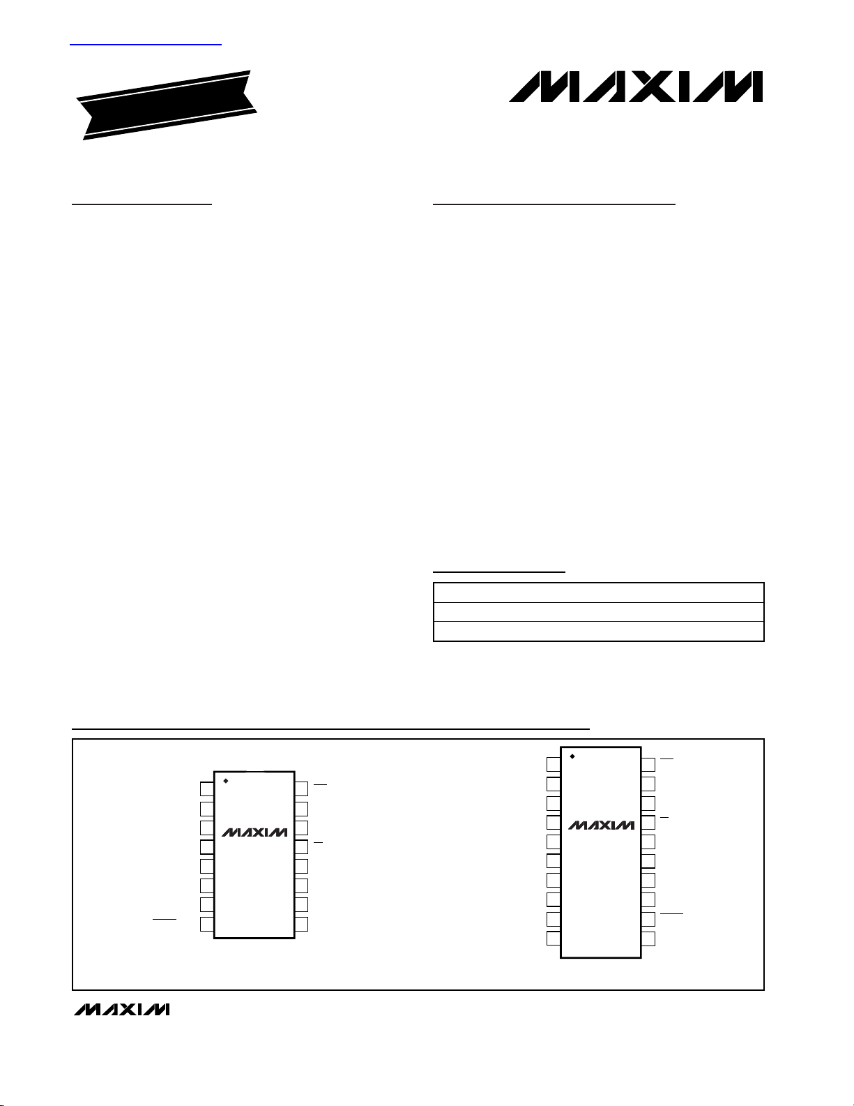
Pin Configurations
19-2853; Rev 1; 7/03
For pricing, delivery, and ordering information, please contact Maxim/Dallas Direct! at
1-888-629-4642, or visit Maxim’s website at www.maxim-ic.com.
EVALUATION KIT
AVAILABLE
Ordering Information
*Future product—contact factory for availability.
Ordering Information continued at end of data sheet.
AutoShutdown is a trademark of Maxim Integrated Products, Inc.
SPI/QSPI are trademarks of Motorola, Inc.
MICROWIRE is a trademark of National Semiconductor Corp.
TOP VIEW
Pin Configurations continued at end of data sheet.
查询MAX1026供应商
PART TEMP RANGE PIN-PACKAGE
MAX1026ACEE-T* 0°C to +70°C 16 QSOP
MAX1026AEEE-T* -40°C to +85°C 16 QSOP
1
AIN0
AIN0
AIN1
AIN2
AIN3
AIN4
AIN5
REF-/AIN6
CNVST/AIN7
1
2
3
MAX1026
4
5
6
7
8
QSOP
16
EOC
15
DOUT
14
DIN
13
CS
12
SCLK
V
11
DD
GND
10
REF+
9
AIN1
AIN2
AIN4
AIN5
AIN6
AIN8
2
3
4
MAX1028
5
6
7
8
9
10
QSOP
20
EOC
19
DOUT
18
DIN
17
CSAIN3
16
SCLK
15
V
14
GND
REF+AIN7
13
12
CNVST/AIN11
11
REF-/AIN10AIN9
DD
Page 2
MAX1026/MAX1028/MAX1030
10-Bit 300ksps ADCs with FIFO,
Temp Sensor, Internal Reference
2 _______________________________________________________________________________________
ABSOLUTE MAXIMUM RATINGS
ELECTRICAL CHARACTERISTICS
(VDD= +5V ±5%, f
SAMPLE
= 300kHz, f
SCLK
= 4.8MHz (50% duty cycle), V
REF
= 4.096V, TA= T
MIN
to T
MAX
, unless otherwise noted.
Typical values are at T
A
= +25°C.)
Stresses beyond those listed under “Absolute Maximum Ratings” may cause permanent damage to the device. These are stress ratings only, and functional
operation of the device at these or any other conditions beyond those indicated in the operational sections of the specifications is not implied. Exposure to
absolute maximum rating conditions for extended periods may affect device reliability.
VDDto GND..............................................................-0.3V to +6V
CS, SCLK, DIN, EOC, DOUT to GND.........-0.3V to (V
DD
+ 0.3V)
AIN0–AIN13, REF-/AIN_, CNVST/AIN_,
REF+ to GND.........................................-0.3V to (V
DD
+ 0.3V)
Maximum Current into Any Pin............................................50mA
Continuous Power Dissipation (T
A
= +70°C)
16-Pin QSOP (derate 8.3mW/°C above +70°C)...........667mW
20-Pin QSOP (derate 9.1mW/°C above +70°C)...........727mW
24-Pin QSOP (derate 9.5mW/°C above +70°C)...........762mW
28-Pin QFN 5mm x 5mm
(derate 20.8mW/°C above +70°C)..........................1667mW
Operating Temperature Ranges
MAX10__C__.......................................................0°C to +70°C
MAX10__E__....................................................-40°C to +85°C
Storage Temperature Range .............................-60°C to +150°C
Junction Temperature......................................................+150°C
Lead Temperature (soldering, 10s) .................................+300°C
DC ACCURACY (Note 1)
Resolution RES 10 Bits
Integral Nonlinearity INL ±1.0 LSB
Differential Nonlinearity DNL No missing codes over temperature ±1.0 LSB
Offset Error ±0.5 ±2.0 LSB
Gain Error (Note 2) ±0.5 ±2.0 LSB
Offset Error Temperature
Coefficient
Gain Temperature Coefficient ±0.8 ppm/°C
Channel-to-Channel Offset
Matching
DYNAMIC SPECIFICATIONS (10kHz sine wave input, 4.096VP-P, 300ksps, fSCLK = 4.8MHz)
Signal-to-Noise Plus Distortion SINAD 70 dB
Total Harmonic Distortion THD Up to the 5th harmonic -82 dBc
Spurious-Free Dynamic Range SFDR 80 dBc
Intermodulation Distortion IMD f
Full-Power Bandwidth -3dB point 1 MHz
Full-Linear Bandwidth S / (N + D) > 68dB 25 kHz
PARAMETER SYMBOL CONDITIONS MIN TYP MAX UNITS
= 9.9kHz, f
in1
= 10.2kHz 76 dBc
in2
±2
±0.1 LSB
ppm/°C
FSR
Page 3
MAX1026/MAX1028/MAX1030
10-Bit 300ksps ADCs with FIFO,
Temp Sensor, Internal Reference
_______________________________________________________________________________________ 3
ELECTRICAL CHARACTERISTICS (continued)
(VDD= +5V ±5%, f
SAMPLE
= 300kHz, f
SCLK
= 4.8MHz (50% duty cycle), V
REF
= 4.096V, TA= T
MIN
to T
MAX
, unless otherwise noted.
Typical values are at T
A
= +25°C.)
CONVERSION RATE
Power-Up Time t
Acquisition Time t
Conversion Time t
External Clock Frequency f
SCLK Duty Cycle 40 60 %
Aperture Delay 30 ns
Aperture Jitter <50 ps
ANALOG INPUT
Input Voltage Range
Input Leakage Current V
Input Capacitance During acquisition time (Note 6) 24 pF
INTERNAL TEMPERATURE SENSOR
Measurement Error (Note 7)
Tem p er atur e M easur em ent N oi se 0.1 °C
Temperature Resolution 1/8 °C
Power-Supply Rejection 0.3 °C/V
INTERNAL REFERENCE
REF Output Voltage 4.024 4.096 4.168 V
REF Temperature Coefficient TC
Output Resistance 6.5 kΩ
REF Output Noise 200 µV
REF Power-Supply Rejection PSRR -70 dB
EXTERNAL REFERENCE INPUT
REF- Input Voltage Range V
REF+ Input Voltage Range V
REF+ Input Current I
PARAMETER SYMBOL CONDITIONS MIN TYP MAX UNITS
PU
ACQ
CONV
SCLK
REF-
REF+
REF+
External reference 0.8
Internal reference (Note 3) 65
Internally clocked 3.5
Externally clocked (Note 4) 2.7
Externally clocked conversion 0.1 4.8
Data I/O 10
Unipolar 0 V
Bipolar (Note 5) - V
= V
IN
DD
Grade A, TA = +25°C ±0.3
Grade A, TA = -20°C to +85°C ±0.5 ±1
Grade A, TA = T
Grade B, TA = +25°C ±0.7
Grade B, T
Grade A ±8
REF
Grade B ±30
V
REF+
V
REF+
A
= 4.096V, f
= 4.096V, f
= T
to T
MIN
to T
MIN
SAMPLE
SAMPLE
MAX
MAX
= 300ksps 40 100
= 0 ±0.1 ±5
RE F
0 500 mV
1.0 VDD + 50mV V
/ 2 V
±0.01 ±1 µA
±0.75 ±1.5
±1.2 ±3.0
RE F
0.6 µs
REF
/ 2
p p m /° C
µs
µs
MHz
V
°C
RMS
RMS
µA
Page 4
MAX1026/MAX1028/MAX1030
10-Bit 300ksps ADCs with FIFO,
Temp Sensor, Internal Reference
4 _______________________________________________________________________________________
Note 1: Tested at VDD= +5V, unipolar input mode.
Note 2: Offset nulled.
Note 3: Time for reference to power up and settle to within 1 LSB.
Note 4: Conversion time is defined as the number of clock cycles multiplied by the clock period; clock has 50% duty cycle.
Note 5: The operational input voltage range for each individual input of a differentially configured pair is from GND to V
DD
. The oper-
ational input voltage difference is from -V
REF
/ 2 to +V
REF
/ 2.
Note 6: See Figure 3 (Input Equivalent Circuit) and the Sampling Error vs. Source Impedance curve in the Typical Operating
Characteristics section.
Note 7: Fast automated test, excludes self-heating effects.
Note 8: Supply current is specified depending on whether an internal or external reference is used for voltage conversions.
Temperature measurements always use the internal reference.
ELECTRICAL CHARACTERISTICS (continued)
(VDD= +5V ±5%, f
SAMPLE
= 300kHz, f
SCLK
= 4.8MHz (50% duty cycle), V
REF
= 4.096V, TA= T
MIN
to T
MAX
, unless otherwise noted.
Typical values are at T
A
= +25°C.)
DIGITAL INPUTS (SCLK, DIN, CS, CNVST)
Input Voltage Low V
Input Voltage High V
Input Hysteresis V
Input Leakage Current I
Input Capacitance C
DIGITAL OUTPUTS (DOUT, EOC)
Output Voltage Low V
Output Voltage High V
Tri-State Leakage Current I
Tri-State Output Capacitance C
POWER REQUIREMENTS
Supply Voltage V
Supply Current (Note 8) I
PARAMETER SYMBOL CONDITIONS MIN TYP MAX UNITS
Power-Supply Rejection PSR VDD = 4.75V to 5.25V; full-scale input ±0.2 ±1 mV
IL
IH
HYST
IN
OL
L
VIN = 0 or V
I
= 2mA 0.4
SINK
I
= 4mA 0.8
SINK
I
CS = V
CS = V
Internal
reference
External
reference
= 1.5mA VDD - 0.5 V
SOURCE
DD
DD
IN
OH
OUT
DD
DD
DD
During temp sense 2400 3100
f
f
Shutdown 0.2 5
During temp sense 1650 2300
f
Shutdown 0.2 5
= 300ksps 1950 2300
SAMPLE
= 0, REF on 1000 1350
SAMPLE
= 300ksps 1250 1500
SAMPLE
2.0 V
4.75 5.25 V
0.8 V
200 mV
±0.01 ±1.0 µA
15 pF
±0.05 ±1 µA
15 pF
V
µA
Page 5
MAX1026/MAX1028/MAX1030
10-Bit 300ksps ADCs with FIFO,
Temp Sensor, Internal Reference
_______________________________________________________________________________________ 5
Note 9: This time is defined as the number of clock cycles needed for conversion multiplied by the clock period. If the internal refer-
ence needs to be powered up, the total time is additive. The internal reference is always used for temperature measurements.
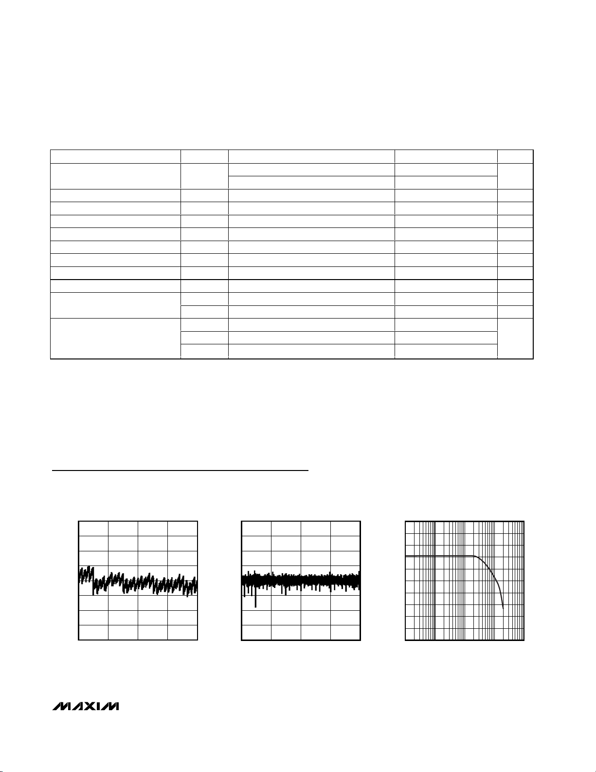
TIMING CHARACTERISTICS (Figure 1)
-0.4
-0.3
-0.2
-0.1
0
0.1
0.2
0.3
0.4
0 256 512 768 1024
INTEGRAL NONLINEARITY
vs. OUTPUT CODE
MAX1026/28/30 toc01
OUTPUT CODE
INTEGRAL NONLINEARITY (LSB)
-0.4
-0.3
-0.2
-0.1
0
0.1
0.2
0.3
0.4
0 256 512 768 1024
DIFFERENTIAL NONLINEARITY
vs. OUTPUT CODE
MAX1026/28/30 toc02
OUTPUT CODE
DIFFERENTIAL NONLINEARITY (LSB)
SINAD vs. FREQUENCY
MAX1026/28/30 toc03
FREQUENCY (kHz)
SINAD AMPLITUDE (dB)
100101
10
20
30
40
50
60
70
80
90
100
0
0.1 1000
Typical Operating Characteristics
(VDD= +5V, V
REF
= +4.096V, f
SCLK
= 4.8MHz, C
LOAD
= 30pF, TA= +25°C, unless otherwise noted.)
SCLK Clock Period t
SCLK Duty Cycle t
SCLK Fall to DOUT Transition t
CS Rise to DOUT Disable t
CS Fall to DOUT Enable t
DIN to SCLK Rise Setup t
SCLK Rise to DIN Hold t
CS to SCLK Rise Setup t
SCLK Rise to CS Hold t
CNVST Pulse Width
CS or CNVST Rise to EOC
Low (Note 9)
PARAMETER SYMBOL CONDITIONS MIN TYP MAX UNITS
CP
CH
DOT
DOD
DOE
DS
DH
CSS
CSH
t
CSW
Externally clocked conversion 208
Data I/O 100
40 60 %
C
= 30pF 40 ns
LOAD
C
= 30pF 40 ns
LOAD
C
= 30pF 40 ns
LOAD
40 ns
0ns
40 ns
0ns
CKSEL = 00, CKSEL = 01 (temp sense) 40 ns
ns
CKSEL = 01 (voltage conversion) 1.4 µs
t
T S
t
R P
Temp sense 55
Voltage conversion 7
Reference power-up 65
µs
Page 6
4.0494
4.0496
4.0495
4.0498
4.0497
4.0499
4.0500
4.75 4.954.85 5.05 5.15 5.25
INTERNAL REFERENCE VOLTAGE
vs. SUPPLY VOLTAGE
MAX1026/28/30 toc10
SUPPLY VOLTAGE (V)
INTERNAL REFERENCE VOLTAGE (V)
MAX1026/MAX1028/MAX1030
10-Bit 300ksps ADCs with FIFO,
Temp Sensor, Internal Reference
6 _______________________________________________________________________________________
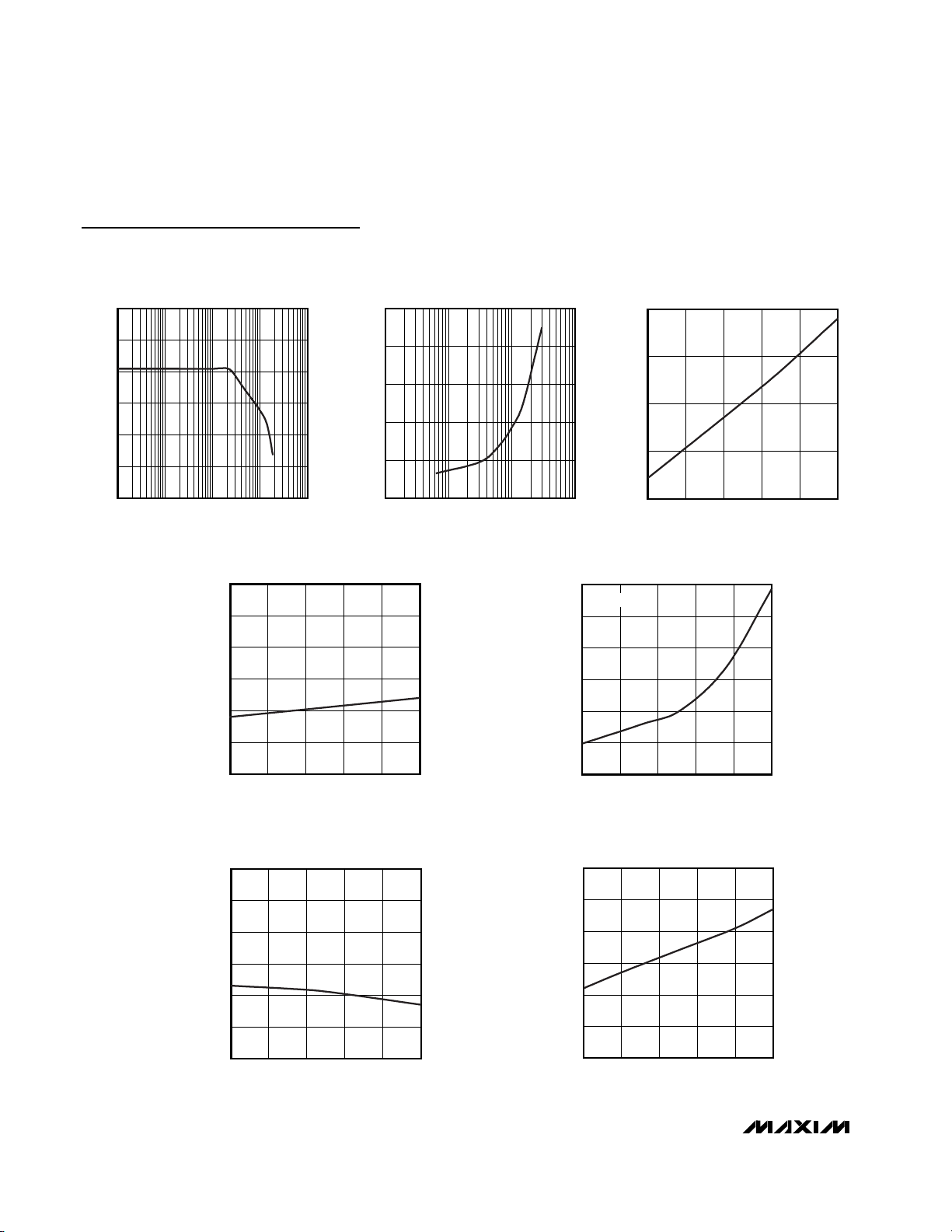
Typical Operating Characteristics (continued)
(VDD= +5V, V
REF
= +4.096V, f
SCLK
= 4.8MHz, C
LOAD
= 30pF, TA= +25°C, unless otherwise noted.)
120
SFDR vs. FREQUENCY
100
80
60
40
SFDR AMPLITUDE (dB)
20
0
0.1 1000
FREQUENCY (kHz)
MAX1026/28/30 toc04
100101
SUPPLY CURRENT vs. SAMPLING RATE
1200
1000
800
600
SUPPLY CURRENT (µA)
400
200
11000
SAMPLING RATE (ksps)
10010
SHUTDOWN SUPPLY CURRENT
vs. SUPPLY VOLTAGE
0.6
0.5
0.4
0.3
MAX1026/28/30 toc07
0.2
SHUTDOWN SUPPLY CURRENT (µA)
0.1
SUPPLY CURRENT vs. SUPPLY VOLTAGE
1200
1150
MAX1026/28/30 toc05
1100
SUPPLY CURRENT (µA)
1050
1000
4.75 5.25
SUPPLY CURRENT vs. TEMPERATURE
1300
fS = 300ksps
1250
1200
1150
1100
SUPPLY CURRENT (µA)
1050
MAX1026/28/30 toc06
5.155.054.954.85
SUPPLY VOLTAGE (V)
MAX1026/28/30 toc08
0
4.75 4.954.85 5.05 5.15 5.25
SUPPLY VOLTAGE (V)
SHUTDOWN SUPPLY CURRENT
vs. TEMPERATURE
0.6
0.5
0.4
0.3
0.2
SHUTDOWN SUPPLY CURRENT (µA)
0.1
0
-40 10-15 35 60 85
TEMPERATURE (°C)
MAX1026/28/30 toc09
1000
-40 85
TEMPERATURE (°C)
603510-15
Page 7
MAX1026/MAX1028/MAX1030
10-Bit 300ksps ADCs with FIFO,
Temp Sensor, Internal Reference
_______________________________________________________________________________________ 7
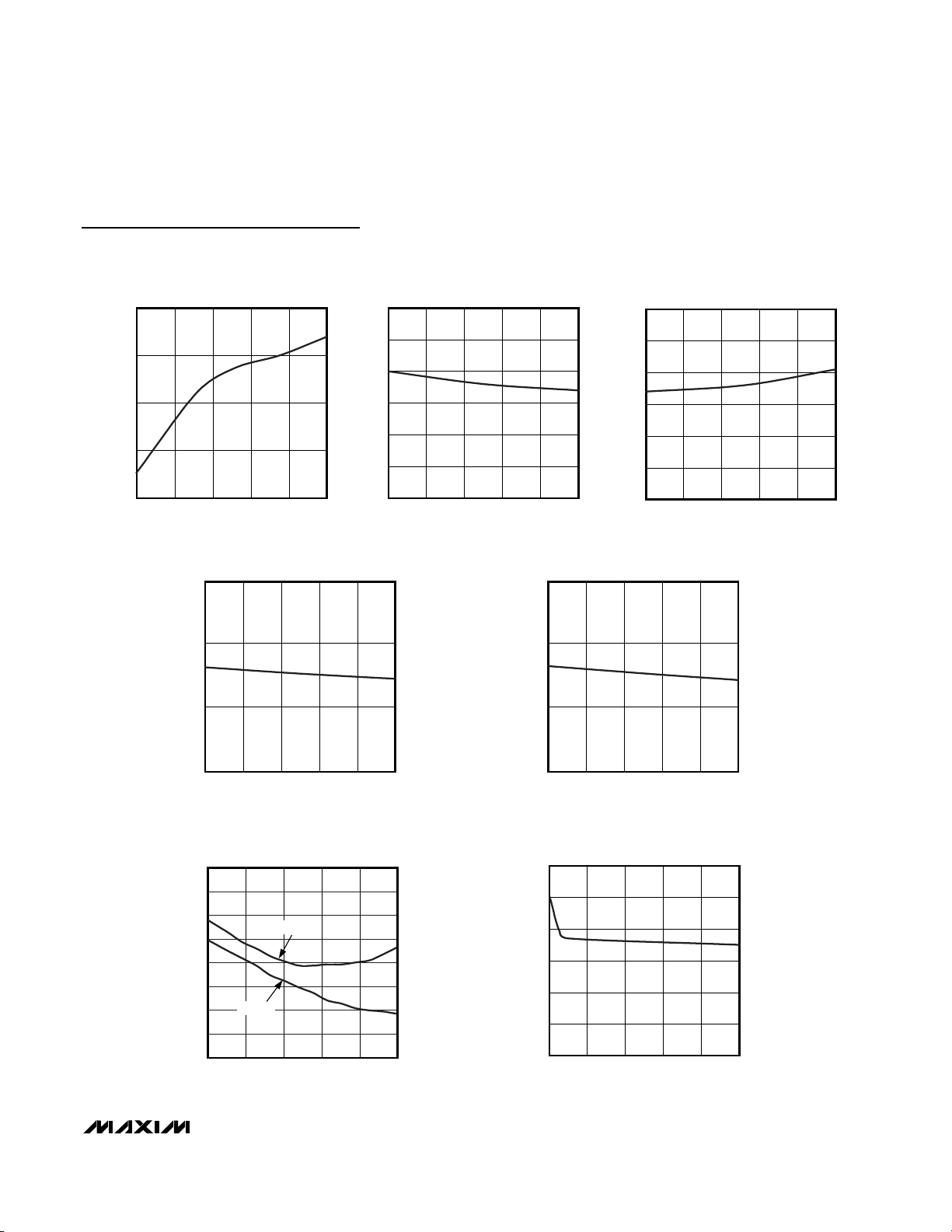
Typical Operating Characteristics (continued)
(VDD= +5V, V
REF
= +4.096V, f
SCLK
= 4.8MHz, C
LOAD
= 30pF, TA= +25°C, unless otherwise noted.)
-1.00
-0.50
0.50
0.25
-0.25
-0.75
0
1.00
0.75
TEMPERATURE SENSOR ERROR
vs. TEMPERATURE
MAX1026/28/30 toc16
TEMPERATURE (°C)
TEMPERATURE SENSOR ERROR (°C)
-40 -15 35 85
6010
GRADE A
GRADE B
-5
-3
-4
-1
-2
0
1
0426810
SAMPLING ERROR
vs. SOURCE IMPEDANCE
MAX1026/28/30 toc17
SOURCE IMPEDANCE (kΩ)
SAMPLING ERROR (LSB)
INTERNAL REFERENCE VOLTAGE
vs. TEMPERATURE
4.051
4.050
4.049
4.048
INTERNAL REFERENCE VOLTAGE (V)
4.047
-40 10-15 356085
0.5
TEMPERATURE (°C)
GAIN ERROR vs. SUPPLY VOLTAGE
0
OFFSET ERROR
vs. SUPPLY VOLTAGE
0.6
0.5
MAX1026/28/30 toc11
0.4
0.3
0.2
OFFSET ERROR (LSB)
0.1
0
4.75 4.954.85 5.05 5.15 5.25
SUPPLY VOLTAGE (V)
MAX1026/28/30 toc14
0.6
0.5
MAX1026/28/30 toc12
0.4
0.3
0.2
OFFSET ERROR (LSB)
0.1
GAIN ERROR vs. TEMPERATURE
0.5
0
0
-40 10-15 35 60 85
OFFSET ERROR
vs. TEMPERATURE
TEMPERATURE (°C)
MAX1026/28/30 toc15
MAX1026/28/30 toc13
GAIN ERROR (LSB)
-0.5
-1.0
4.75 4.85 5.05 5.25
SUPPLY VOLTAGE (V)
GAIN ERROR (LSB)
-0.5
-1.0
5.154.95
-40 -15 35 85
TEMPERATURE (°C)
6010
Page 8
MAX1026/MAX1028/MAX1030
10-Bit 300ksps ADCs with FIFO,
Temp Sensor, Internal Reference
8 _______________________________________________________________________________________
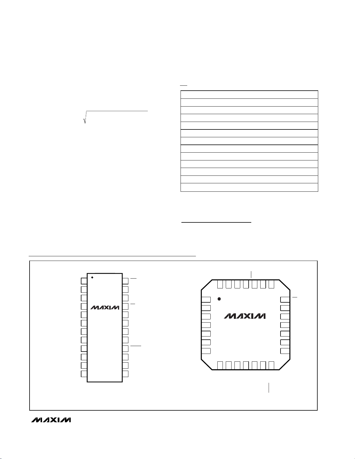
Pin Description
MAX1030
QFN
1, 17, 19,
25
2–12, 26,
27, 28
——1–10 — AIN0–9 Analog Inputs
———1–6AIN0–5 Analog Inputs
13 15 ——REF-/AIN14
——11 — REF-/AIN10
——— 7 REF-/AIN6
14 16 ——
——12 —
——— 8
15 17 13 9 REF+ Positive Reference Input. Bypass to GND with a 0.1µF capacitor.
16 18 14 10 GND Ground
18 19 15 11 V
20 20 16 12 SCLK
MAX1030
QSOP
———N.C. No Connection. Not internally connected.
1–14 ——AIN0–13 Analog Inputs
MAX1028 MAX1026 NAME FUNCTION
Negative Input for External Differential Reference/Analog Input 14.
See Table 3 for details on programming the setup register.
Negative Input for External Differential Reference/Analog Input 10.
See Table 3 for details on programming the setup register.
Negative Input for External Differential Reference/Analog Input 6.
See Table 3 for details on programming the setup register.
CNVST/
AIN15
CNVST/
AIN11
CNVST/
AIN7
DD
Active-Low Conversion Start Input/Analog Input 15. See Table 3
for details on programming the setup register.
Active-Low Conversion Start Input/Analog Input 11. See Table 3
for details on programming the setup register.
Active-Low Conversion Start Input/Analog Input 7. See Table 3 for
details on programming the setup register.
Power Input. Bypass to GND with a 0.1µF capacitor.
Serial Clock Input. Clocks data in and out of the serial interface.
(Duty cycle must be 40% to 60%.) See Table 3 for details on
programming the clock mode.
21 21 17 13 CS
22 22 18 14 DIN
23 23 19 15 DOUT
24 24 20 16 EOC End of Conversion Output. Data is valid after EOC pulls low.
Active-Low Chip-Select Input. When CS is low, the serial interface
is enabled. When CS is high, DOUT is high impedance.
Serial Data Input. DIN data is latched into the serial interface on
the rising edge of SCLK.
Serial Data Output. Data is clocked out on the falling edge of
SCLK. High impedance when CS is connected to V
DD
.
Page 9
MAX1026/MAX1028/MAX1030
10-Bit 300ksps ADCs with FIFO,
Temp Sensor, Internal Reference
_______________________________________________________________________________________ 9
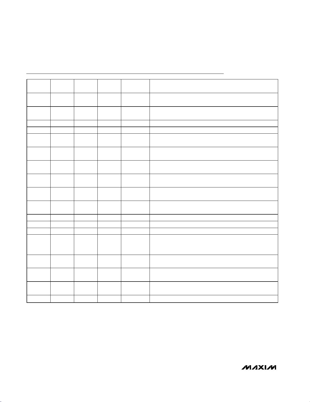
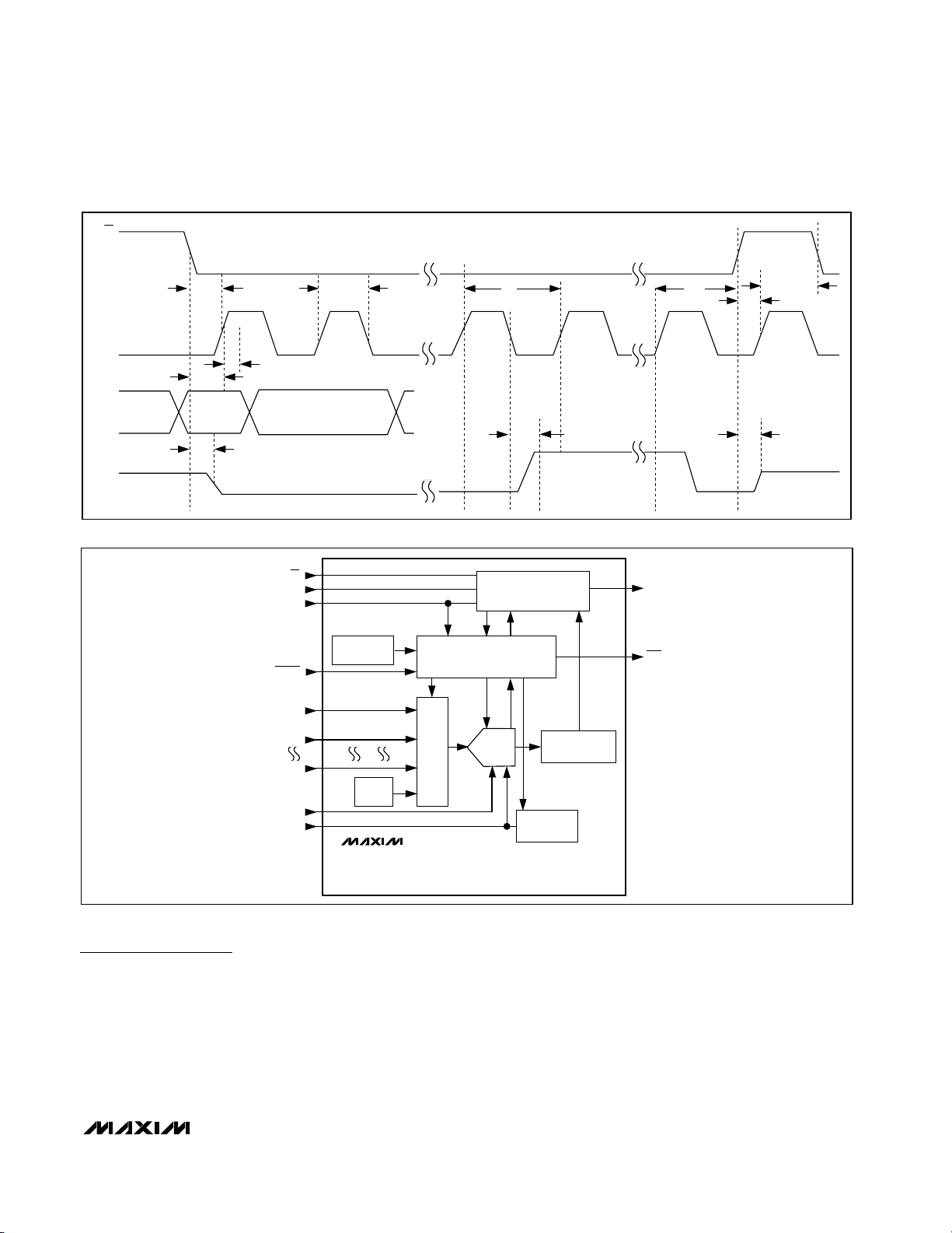
Detailed Description
The MAX1026/MAX1028/MAX1030 are low-power, serial-output, multichannel ADCs with temperature-sensing
capability for temperature-control, process-control, and
monitoring applications. These 10-bit ADCs have internal track and hold (T/H) circuitry that supports singleended and fully differential inputs. Data is converted
from an internal temperature sensor or analog voltage
sources in a variety of channel and data-acquisition
configurations. Microprocessor (µP) control is made
easy through a 3-wire SPI/QSPI/MICROWIRE-compatible serial interface.
Figure 2 shows a simplified functional diagram of the
MAX1026/MAX1028/MAX1030 internal architecture. The
MAX1026 has eight single-ended analog input channels or four differential channels. The MAX1028 has 12
single-ended analog input channels or six differential
channels. The MAX1030 has 16 single-ended analog
input channels or eight differential channels.
Figure 1. Detailed Serial-Interface Timing Diagram
Figure 2. Functional Diagram
CS
t
CH
SCLK
DIN
DOUT
t
CSS
t
t
DS
DH
t
DOE
CS
DIN
SCLK
OSCILLATOR
CNVST
t
DOT
CONTROL
t
CP
SERIAL
INTERFACE
DOUT
EOC
t
CSH
t
CSH
t
CSS
t
DOD
AIN1
AIN2
AIN15
REFREF+
TEMP
SENSE
MAX1026
MAX1028
MAX1030
T/H
12-BIT
SAR
ADC
ACCUMULATOR
INTERNAL
REFERENCE
FIFO AND
Page 10

MAX1026/MAX1028/MAX1030
10-Bit 300ksps ADCs with FIFO,
Temp Sensor, Internal Reference
10 ______________________________________________________________________________________
Converter Operation
The MAX1026/MAX1028/MAX1030 ADCs use a fully differential, successive-approximation register (SAR) conversion technique and an on-chip T/H block to convert
temperature and voltage signals into a 10-bit digital
result. Both single-ended and differential configurations
are supported, with a unipolar signal range for singleended mode and bipolar or unipolar ranges for differential mode.
Input Bandwidth
The ADC’s input-tracking circuitry has a 1MHz smallsignal bandwidth, so it is possible to digitize highspeed transient events and measure periodic signals
with bandwidths exceeding the ADC’s sampling rate by
using undersampling techniques. Anti-alias prefiltering
of the input signals is necessary to avoid high-frequency signals aliasing into the frequency band of interest.
Analog Input Protection
Internal ESD protection diodes clamp all pins to V
DD
and GND, allowing the inputs to swing from (GND -
0.3V) to (VDD+ 0.3V) without damage. However, for
accurate conversions near full scale, the inputs must
not exceed VDDby more than 50mV or be lower than
GND by 50mV. If an off-channel analog input voltage
exceeds the supplies, limit the input current to 2mA.
3-Wire Serial Interface
The MAX1026/MAX1028/MAX1030 feature a serial
interface compatible with SPI/QSPI and MICROWIRE
devices. For SPI/QSPI, ensure the CPU serial interface
runs in master mode so it generates the serial clock
signal. Select the SCLK frequency of 10MHz or less,
and set clock polarity (CPOL) and phase (CPHA) in the
µP control registers to the same value. The MAX1026/
MAX1028/MAX1030 operate with SCLK idling high or
low, and thus operate with CPOL = CPHA = 0 or CPOL
= CPHA = 1. Set CS low to latch input data at DIN on
the rising edge of SCLK. Output data at DOUT is
updated on the falling edge of SCLK. Bipolar true-differential results and temperature sensor results are
available in two’s complement format, while all others
are in binary.
Serial communication always begins with an 8-bit input
data byte (MSB first) loaded from DIN. Send a second
byte, immediately following the setup byte, to write to
the unipolar mode or bipolar mode registers (see
Tables 1, 3, 4, and 5). A high-to-low transition on CS initiates the data input operation. The input data byte and
the subsequent data bytes are clocked from DIN into
the serial interface on the rising edge of SCLK.
Tables 1–7 detail the register descriptions. Bits 5 and 4,
CKSEL1 and CKSEL0, respectively, control the clock
modes in the setup register (see Table 3). Choose
between four different clock modes for various ways to
start a conversion and determine whether the acquisitions are internally or externally timed. Select clock
mode 00 to configure CNVST/AIN_ to act as a conversion start and use it to request the programmed internally timed conversions without tying up the serial bus.
In clock mode 01, use CNVST to request conversions
one channel at a time, controlling the sampling speed
without tying up the serial bus. Request and start internally timed conversions through the serial interface by
writing to the conversion register in the default clock
mode, 10. Use clock mode 11 with SCLK up to 4.8MHz
for externally timed acquisitions to achieve sampling
rates up to 300ksps. Clock mode 11 disables scanning
and averaging. See Figures 4–7 for timing specifications and how to begin a conversion.
These devices feature an active-low, end-of-conversion
output. EOC goes low when the ADC completes the
last-requested operation and is waiting for the next
input data byte (for clock modes 00 and 10). For clock
mode 01, EOC goes low after the ADC completes each
requested operation. EOC goes high when CS or CNVST
goes low. EOC is always high in clock mode 11.
Single-Ended/Differential Input
The MAX1026/MAX1028/MAX1030 use a fully differential ADC for all conversions. The analog inputs can be
configured for either differential or single-ended conversions by writing to the setup register (see Table 3).
Single-ended conversions are internally referenced to
GND (see Figure 3).
In differential mode, the T/H samples the difference
between two analog inputs, eliminating common-mode
DC offsets and noise. IN+ and IN- are selected from
the following pairs: AIN0/AIN1, AIN2/AIN3, AIN4/AIN5,
AIN6/AIN7, AIN8/AIN9, AIN10/AIN11, AIN12/AIN13,
and AIN14/AIN15. AIN0–AIN7 are available on the
MAX1026, MAX1028, and MAX1030. AIN8–AIN11 are
only available on the MAX1028 and MAX1030.
AIN12–AIN15 are only available on the MAX1030. See
Tables 2–5 for more details on configuring the inputs.
For the inputs that can be configured as CNVST or an
analog input, only one can be used at a time. For the
inputs that can be configured as REF- or an analog
input, the REF- configuration excludes the analog input.
Page 11

MAX1026/MAX1028/MAX1030
10-Bit 300ksps ADCs with FIFO,
Temp Sensor, Internal Reference
______________________________________________________________________________________ 11
Unipolar/Bipolar
Address the unipolar and bipolar registers through the
setup register (bits 1 and 0). Program a pair of analog
channels for differential operation by writing a 1 to the
appropriate bit of the bipolar or unipolar register.
Unipolar mode sets the differential input range from 0 to
V
REF
. A negative differential analog input in unipolar
mode causes the digital output code to be zero.
Selecting bipolar mode sets the differential input range
to ±V
REF
/ 2. The digital output code is binary in unipolar mode and two’s complement in bipolar mode (see
the transfer function graphs, Figures 8 and 9).
In single-ended mode, the MAX1026/MAX1028/
MAX1030 always operate in unipolar mode. The analog
inputs are internally referenced to GND with a full-scale
input range from 0 to V
REF
.
True Differential Analog Input T/H
The equivalent circuit of Figure 3 shows the
MAX1026/MAX1028/MAX1030s’ input architecture. In
track mode, a positive input capacitor is connected to
AIN0–AIN15 in single-ended mode (and AIN0, AIN2,
AIN4…AIN14 in differential mode). A negative input
capacitor is connected to GND in single-ended mode
(or AIN1, AIN3, AIN5…AIN15 in differential mode). For
external track-and-hold timing, use clock mode 01.
After the T/H enters hold mode, the difference between
the sampled positive and negative input voltages is
converted. The time required for the T/H to acquire an
input signal is determined by how quickly its input
capacitance is charged. If the input signal’s source
impedance is high, the required acquisition time lengthens. The acquisition time, t
ACQ
, is the maximum time
needed for a signal to be acquired, plus the power-up
time. It is calculated by the following equation:
where R
IN
= 1.5kΩ, RSis the source impedance of the
input signal, and t
PWR
= 1µs, the power-up time of the
device. The varying power-up times are detailed in the
explanation of the clock mode conversions.
t
ACQ
is never less than 1.4µs, and any source imped-
ance below 300Ω does not significantly affect the
ADC’s AC performance. A high-impedance source can
be accommodated either by lengthening t
ACQ
or by
placing a 1µF capacitor between the positive and negative analog inputs.
Internal FIFO
The MAX1026/MAX1028/MAX1030 contain a FIFO
buffer that can hold up to 16 ADC results plus one temperature result. This allows the ADC to handle multiple
internally clocked conversions and a temperature measurement, without tying up the serial bus.
If the FIFO is filled and further conversions are requested without reading from the FIFO, the oldest ADC
results are overwritten by the new ADC results. Each
result contains 2 bytes, with the MSB preceded by 4
leading zeros and the LSB followed by 2 sub-bits. After
each falling edge of CS, the oldest available byte of
data is available at DOUT, MSB first. When the FIFO is
empty, DOUT is zero.
The first 2 bytes of data read out after a temperature measurement always contain the temperature result preceded
by 4 leading zeros, MSB first. If another temperature measurement is performed before the first temperature result
is read out, the old measurement is overwritten by the
new result. Temperature results are in degrees Celsius
(two’s complement) at a resolution of 1/8 of a degree. See
the Temperature Measurements section for details on
converting the digital code to a temperature.
Internal Clock
The MAX1026/MAX1028/MAX1030 operate from an internal oscillator, which is accurate within 10% of the
4.4MHz nominal clock rate. The internal oscillator is
active in clock modes 00, 01, and 10. Read out the data
at clock speeds up to 10MHz. See Figures 4–7 for details
on timing specifications and starting a conversion.
txRRxpFt
AQC S IN PWR
=+
()
+924
Figure 3. Equivalent Input Circuit
AIN0-AIN15
(SINGLE ENDED);
AIN0, AIN2,
AIN4…AIN14
(DIFFERENTIAL)
HOLD
GND
(SINGLE ENDED);
AIN1, AIN3,
AIN5…AIN15
(DIFFERENTIAL)
REF
GND
CIN+
CIN-
HOLD
V
DD
DAC
COMPARATOR
+
-
HOLD
/2
Page 12

MAX1026/MAX1028/MAX1030
10-Bit 300ksps ADCs with FIFO,
Temp Sensor, Internal Reference
12 ______________________________________________________________________________________
Applications Information
Register Descriptions
The MAX1026/MAX1028/MAX1030 communicate
between the internal registers and the external circuitry
through the SPI/QSPI-compatible serial interface. Table
1 details the registers and the bit names. Tables 2–7
show the various functions within the conversion register, setup register, averaging register, reset register,
unipolar register, and bipolar register.
Conversion Time Calculations
The conversion time for each scan is based on a number of different factors: conversion time per sample,
samples per result, results per scan, if a temperature
measurement is requested, and if the external reference is in use.
Use the following formula to calculate the total conversion time for an internally timed conversion in clock
modes 00 and 10 (see the Electrical Characteristics
section as applicable):
total conversion time = t
cnv
x n
avg
x n
result
+ t
TS
+ t
RP
where:
t
cnv
= t
acq
(max) + t
conv
(max)
n
avg
= samples per result (amount of averaging)
n
result
= number of FIFO results requested; determined
by number of channels being scanned or by NSCAN1,
NSCAN0
tTS= time required for temperature measurement; set
to zero if temp measurement is not requested
t
RP
= internal reference wake-up; set to zero if the internal reference is already powered up or if the external
reference is being used
In clock mode 01, the total conversion time depends on
how long CNVST is held low or high, including any time
required to turn on the internal reference. Conversion
time in externally clocked mode (CKSEL1, CKSEL0 = 11)
depends on the SCLK period and how long CS is held
high between each set of eight SCLK cycles.
Conversion Register
Select active analog input channels, scan modes, and
a single temperature measurement per scan by writing
to the conversion register. Table 2 details channel
selection, the four scan modes, and how to request a
temperature measurement. Request a scan by writing
to the conversion register when in clock mode 10 or 11,
or by applying a low pulse to the CNVST pin when in
clock mode 00 or 01.
A conversion is not performed if it is requested on a
channel that has been configured as CNVST or REF-.
Do not request conversions on channels 8–15 on the
MAX1026 and channels 12–15 on the MAX1028. Set
CHSEL3:CHSEL0 to the lower channel’s binary value. If
the last two channels are configured as a differential
pair and one of them has been reconfigured as CNVST
or REF-, the pair is ignored.
Select scan mode 00 or 01 to return one result per single-ended channel and one result per differential pair
within the requested range, plus one temperature result if
selected. Select scan mode 10 to scan a single input
channel numerous times, depending on NSCAN1 and
NSCAN0 in the averaging register (Table 6). Select scan
mode 11 to return only one result from a single channel.
Table 1. Input Data Byte (MSB First)
*Unipolar/bipolar channels 8–15 are only valid on the MAX1028 and MAX1030.
**Unipolar/bipolar channels 12–15 are only valid on the MAX1030.
X = Don’t care.
REGISTER NAME BIT 7 BIT 6 BIT 5 BIT 4 BIT 3 BIT 2 BIT 1 BIT 0
Conversion 1 CHSEL3 CHSEL2 CHSEL1 CHSEL0 SCAN1 SCAN0 TEMP
Setup 0 1 CKSEL1 CKSEL0 REFSEL1 REFSEL0 DIFFSEL1 DIFFSEL0
Averaging 0 0 1 AVGON NAVG1 NAVG0 NSCAN1 NSCAN0
Reset 0 0 0 1 RESET XXX
Unipolar mode (setup) UCH0/1 UCH2/3 UCH4/5 UCH6/7 UCH8/9* UCH10/11* UCH12/13** UCH14/15**
Bipolar mode (setup) BCH0/1 BCH1/2 BCH4/5 BCH6/7 BCH8/9* BCH10/11* BCH12/13** BCH14/15**
Page 13
MAX1026/MAX1028/MAX1030
10-Bit 300ksps ADCs with FIFO,
Temp Sensor, Internal Reference
______________________________________________________________________________________ 13
Setup Register
Write a byte to the setup register to configure the clock,
reference, and power-down modes. Table 3 details the
bits in the setup register. Bits 5 and 4 (CKSEL1 and
CKSEL0) control the clock mode, acquisition and sampling, and the conversion start. Bits 3 and 2 (REFSEL1
and REFSEL0) control internal or external reference use.
Bits 1 and 0 (DIFFSEL1 and DIFFSEL0) address the
unipolar mode and bipolar mode registers and configure
the analog input channels for differential operation.
Unipolar/Bipolar Registers
The final 2 bits (LSBs) of the setup register control the
unipolar/bipolar mode address registers. Set bits 1 and
0 (DIFFSEL1 and DIFFSEL0) to 10 to write to the unipolar mode register. Set bits 1 and 0 to 11 to write to the
bipolar mode register. In both cases, the setup byte
must be followed immediately by 1 byte of data written
to the unipolar register or bipolar register. Hold CS low
and run 16 SCLK cycles before pulling CS high. If the
last 2 bits of the setup register are 00 or 01, neither the
unipolar mode register nor the bipolar mode register is
written. Any subsequent byte is recognized as a new
input data byte. See Tables 4 and 5 to program the
unipolar and bipolar mode registers.
If a channel is configured as both unipolar and bipolar,
the unipolar setting takes precedence. In unipolar
mode, AIN+ can exceed AIN- by up to V
REF
. The output format in unipolar mode is binary. In bipolar mode,
either input can exceed the other by up to V
REF
/ 2. The
output format in bipolar mode is two's complement.
Averaging Register
Write to the averaging register to configure the ADC to
average up to 32 samples for each requested result,
and to independently control the number of results
requested for single-channel scans.
Table 2 details the four scan modes available in the conversion register. All four scan modes allow averaging as
long as the AVGON bit, bit 4 in the averaging register, is
set to 1. Select scan mode 10 to scan the same channel
multiple times. Clock mode 11 disables averaging.
Reset Register
Write to the reset register (as shown in Table 7) to clear
the FIFO or to reset all registers to their default states.
Set the RESET bit to 1 to reset the FIFO. Set the reset
bit to zero to return the MAX1026/MAX1028/MAX1030
to the default power-up state.
Table 2. Conversion Register*
*See below for bit details.
BIT
NAME
— 7 (MSB) Set to 1 to select conversion register.
CHSEL3 6 Analog input channel select.
CHSEL2 5 Analog input channel select.
CHSEL1 4 Analog input channel select.
CHSEL0 3 Analog input channel select.
SCAN1 2 Scan mode select.
SCAN0 1 Scan mode select.
TEMP 0 (LSB)
CHSEL3 CHSEL2 CHSEL1 CHSEL0
SCAN1 SCAN0
0 0 Scans channels 0 through N.
01
10
1 1 No scan. Converts channel N once only.
BIT FUNCTION
Set to 1 to take a single temperature
measurement. The first conversion result
of a scan contains temperature information.
SELECTED
CHANNEL (N)
0 0 0 0 AIN0
0 0 0 1 AIN1
0 0 1 0 AIN2
0 0 1 1 AIN3
0 1 0 0 AIN4
0 1 0 1 AIN5
0 1 1 0 AIN6
0 1 1 1 AIN7
1 0 0 0 AIN8
1 0 0 1 AIN9
1 0 1 0 AIN10
1 0 1 1 AIN11
1 1 0 0 AIN12
1 1 0 1 AIN13
1 1 1 0 AIN14
1 1 1 1 AIN15
SCAN MODE (CHANNEL N IS
SELECTED BY BITS CHSEL3–CHSEL0)
Scans channels N through the highest
numbered channel.
S cans channel N r ep eated l y. The aver ag i ng
r eg i ster sets the num b er of r esul ts.
Page 14

MAX1026/MAX1028/MAX1030
10-Bit 300ksps ADCs with FIFO,
Temp Sensor, Internal Reference
14 ______________________________________________________________________________________
Table 3. Setup Register*
*See below for bit details.
BIT NAME BIT FUNCTION
— 7 (MSB) Set to zero to select setup register.
— 6 Set to 1 to select setup register.
CKSEL1 5 Clock mode and CNVST configuration. Resets to 1 at power-up.
CKSEL0 4 Clock mode and CNVST configuration.
REFSEL1 3 Reference mode configuration.
REFSEL0 2 Reference mode configuration.
DIFFSEL1 1 Unipolar/bipolar mode register configuration for differential mode.
DIFFSEL0 0 (LSB) Unipolar/bipolar mode register configuration for differential mode.
CKSEL1 CKSEL0 CONVERSION CLOCK ACQUISITION/SAMPLING CNVST CONFIGURATION
0 0 Internal Internally timed
0 1 Internal Externally timed through CNVST CNVST
1 0 Internal Internally timed AIN15/11/7
1 1 External (4.8MHz max) Externally timed through SCLK AIN15/11/7
CNVST
REFSEL1 REFSEL0 VOLTAGE REFERENCE AutoShutdown REF- CONFIGURATION
0 0 Internal
0 1 External single ended Reference off; no wake-up delay. AIN14/10/6
1 0 Internal
1 1 External differential Reference off; no wake-up delay. REF-
DIFFSEL1 DIFFSEL0 FUNCTION
0 0 No data follows the setup byte. Unipolar mode and bipolar mode registers remain unchanged.
0 1 No data follows the setup byte. Unipolar mode and bipolar mode registers remain unchanged.
1 0 One byte of data follows the setup byte and is written to the unipolar mode register.
1 1 One byte of data follows the setup byte and is written to the bipolar mode register.
Reference off after scan; need
wake-up delay.
Reference always on; no wake-up
delay.
AIN14/10/6
AIN14/10/6
Page 15

MAX1026/MAX1028/MAX1030
10-Bit 300ksps ADCs with FIFO,
Temp Sensor, Internal Reference
______________________________________________________________________________________ 15
Power-Up Default State
The MAX1026/MAX1028/MAX1030 power up with all
blocks in shutdown, including the reference. All registers
power up in state 00000000, except for the setup register, which powers up in clock mode 10 (CKSEL1 = 1).
Temperature Measurements
The MAX1026/MAX1028/MAX1030 perform temperature measurements with an internal diode-connected
transistor. The diode bias current changes from 68µA
to 4µA to produce a temperature-dependent bias voltage difference. The second conversion result at 4µA is
subtracted from the first at 68µA to calculate a digital
value that is proportional to absolute temperature. The
output data appearing at DOUT is the above digital
code minus an offset to adjust from Kelvin to Celsius.
The reference voltage used for the temperature measurements is derived from the internal reference source
to ensure a resolution of 1/8 of a degree.
Output Data Format
Figures 4–7 illustrate the conversion timing for the
MAX1026/MAX1028/MAX1030. The 10-bit conversion
result is output in MSB-first format with 4 leading zeros
and 2 trailing sub-bits. The 12-bit temperature measurement is output with 4 leading zeros. DIN data is
latched into the serial interface on the rising edge of
SCLK. Data on DOUT transitions on the falling edge of
SCLK. Conversions in clock modes 00 and 01 are initiated by CNVST. Conversions in clock modes 10 and 11
are initiated by writing an input data byte to the conversion register. Data is binary for unipolar mode and two’s
complement for bipolar mode.
Table 4. Unipolar Mode Register (Addressed Through Setup Register)
Table 5. Bipolar Mode Register (Addressed Through Setup Register)
BIT NAME BIT FUNCTION
UCH0/1 7 (MSB) Set to 1 to configure AIN0 and AIN1 for unipolar differential conversion.
UCH2/3 6 Set to 1 to configure AIN2 and AIN3 for unipolar differential conversion.
UCH4/5 5 Set to 1 to configure AIN4 and AIN5 for unipolar differential conversion.
UCH6/7 4 Set to 1 to configure AIN6 and AIN7 for unipolar differential conversion.
UCH8/9 3 Set to 1 to configure AIN8 and AIN9 for unipolar differential conversion (MAX1028/MAX1030 only).
UCH10/11 2 Set to 1 to configure AIN10 and AIN11 for unipolar differential conversion (MAX1028/MAX1030 only).
UCH12/13 1 Set to 1 to configure AIN12 and AIN13 for unipolar differential conversion (MAX1030 only).
UCH14/15 0 (LSB) Set to 1 to configure AIN14 and AIN15 for unipolar differential conversion (MAX1030 only).
BIT NAME BIT FUNCTION
BCH0/1 7 (MSB) Set to 1 to configure AIN0 and AIN1 for bipolar differential conversion.
BCH2/3 6 Set to 1 to configure AIN2 and AIN3 for bipolar differential conversion.
BCH4/5 5 Set to 1 to configure AIN4 and AIN5 for bipolar differential conversion.
BCH6/7 4 Set to 1 to configure AIN6 and AIN7 for bipolar differential conversion.
BCH8/9 3 Set to 1 to configure AIN8 and AIN9 for bipolar differential conversion (MAX1028/MAX1030 only).
BCH10/11 2 Set to 1 to configure AIN10 and AIN11 for bipolar differential conversion (MAX1028/MAX1030 only).
BCH12/13 1 Set to 1 to configure AIN12 and AIN13 for bipolar differential conversion (MAX1030 only).
BCH14/15 0 (LSB) Set to 1 to configure AIN14 and AIN15 for bipolar differential conversion (MAX1030 only).
Page 16
MAX1026/MAX1028/MAX1030
10-Bit 300ksps ADCs with FIFO,
Temp Sensor, Internal Reference
16 ______________________________________________________________________________________
Table 6. Averaging Register*
Table 7. Reset Register
*See below for bit details.
BIT NAME BIT FUNCTION
— 7 (MSB) Set to zero to select averaging register.
— 6 Set to zero to select averaging register.
— 5 Set to 1 to select averaging register.
AVGON 4 Set to 1 to turn averaging on. Set to zero to turn averaging off.
NAVG1 3 Configures the number of conversions for single-channel scans.
NAVG0 2
NSCAN1 1 Single-channel scan count. (Scan mode 10 only.)
NSCAN0 0 (LSB) Single-channel scan count. (Scan mode 10 only.)
AVGON NAVG1 NAVG0 FUNCTION
0 x x Performs 1 conversion for each requested result.
1 0 0 Performs 4 conversions and returns the average for each requested result.
1 0 1 Performs 8 conversions and returns the average for each requested result.
1 1 0 Performs 16 conversions and returns the average for each requested result.
1 1 1 Performs 32 conversions and returns the average for each requested result.
Configures the number of conversions for single-channel scans.
NSCAN1 NSCAN0 FUNCTION (APPLIES ONLY IF SCAN MODE 10 IS SELECTED)
0 0 Scans channel N and returns 4 results.
0 1 Scans channel N and returns 8 results.
1 0 Scans channel N and returns 12 results.
1 1 Scans channel N and returns 16 results.
BIT NAME BIT FUNCTION
— 7 (MSB) Set to zero to select reset register.
— 6 Set to zero to select reset register.
— 5 Set to zero to select reset register.
— 4 Set to 1 to select reset register.
RESET 3 Set to zero to reset all registers. Set to 1 to clear the FIFO only.
x 2 Reserved. Don’t care.
x 1 Reserved. Don’t care.
x 0 (LSB) Reserved. Don’t care.
Page 17

MAX1026/MAX1028/MAX1030
10-Bit 300ksps ADCs with FIFO,
Temp Sensor, Internal Reference
______________________________________________________________________________________ 17
Internally Timed Acquisitions and
Conversions Using
CNVST
Performing Conversions in Clock Mode 00
In clock mode 00, the wake up, acquisition, conversion,
and shutdown sequences are initiated through CNVST
and performed automatically using the internal oscillator. Results are added to the internal FIFO to be read
out later. See Figure 4 for clock mode 00 timing.
Initiate a scan by setting CNVST low for at least 40ns
before pulling it high again. The MAX1026/MAX1028/
MAX1030 then wake up, scan all requested channels,
store the results in the FIFO, and shut down. After the
scan is complete, EOC is pulled low and the results are
available in the FIFO. Wait until EOC goes low before
pulling CS low to communicate with the serial interface.
EOC stays low until CS or CNVST is pulled low again. A
temperature measurement result, if requested, precedes all other FIFO results.
Do not initiate a second CNVST before EOC goes low;
otherwise, the FIFO can become corrupted.
Externally Timed Acquisitions and
Internally Timed Conversions with
CNVST
Performing Conversions in Clock Mode 01
In clock mode 01, conversions are requested one at a
time using CNVST and performed automatically using
the internal oscillator. See Figure 5 for clock mode 01
timing.
Setting CNVST low begins an acquisition, wakes up the
ADC, and places it in track mode. Hold CNVST low for
at least 1.4µs to complete the acquisition. If the internal
reference needs to wake up, an additional 65µs is
required for the internal reference to power up. If a temperature measurement is being requested, reference
power-up and temperature measurement are internally
timed. In this case, hold CNVST low for at least 40ns.
Set CNVST high to begin a conversion. After the con-
version is complete, the ADC shuts down and pulls
EOC low. EOC stays low until CS or CNVST is pulled
low again. Wait until EOC goes low before pulling CS or
CNVST low.
If averaging is turned on, multiple CNVST pulses need
to be performed before a result is written to the FIFO.
Once the proper number of conversions has been performed to generate an averaged FIFO result, as specified by the averaging register, the scan logic
automatically switches the analog input multiplexer to
the next-requested channel. If a temperature measurement is programmed, it is performed after the first rising
edge of CNVST following the input data byte written to
the conversion register. The result is available on DOUT
once EOC has been pulled low.
Figure 4. Clock Mode 00
CNVST
CS
SCLK
DOUT
EOC
SET CNVST LOW FOR AT LEAST 40ns TO BEGIN A CONVERSION. X = DON'T CARE.
(UP TO 514 INTERNALLY CLOCKED ACQUISITIONS AND CONVERSIONS)
MSB1
LSB1 MSB2
Page 18

MAX1026/MAX1028/MAX1030
10-Bit 300ksps ADCs with FIFO,
Temp Sensor, Internal Reference
18 ______________________________________________________________________________________
Internally Timed Acquisitions and
Conversions Using the Serial Interface
Performing Conversions in Clock Mode 10
In clock mode 10, the wake-up, acquisition, conversion,
and shutdown sequences are initiated by writing an
input data byte to the conversion register, and are performed automatically using the internal oscillator. This
is the default clock mode upon power-up. See Figure 6
for clock mode 10 timing.
Initiate a scan by writing a byte to the conversion register. The MAX1026/MAX1028/MAX1030 then power up,
scan all requested channels, store the results in the
FIFO, and shut down. After the scan is complete, EOC
is pulled low and the results are available in the FIFO. If
a temperature measurement is requested, the temperature result precedes all other FIFO results. EOC stays
low until CS is pulled low again.
Figure 5. Clock Mode 01
Figure 6. Clock Mode 10
CNVST
(ACQUISITION1)
CS
SCLK
DOUT
EOC
DIN
CS
SCLK
(CONVERSION1)
REQUEST MULTIPLE CONVERSIONS BY SETTING CNVST LOW FOR EACH CONVERSION. X = DON'T CARE.
(ACQUISITION2)
(CONVERSION2)
MSB1
(CONVERSION BYTE)
(UP TO 514 INTERNALLY CLOCKED ACQUISITIONS AND CONVERSIONS)
DOUT
MSB1
LSB1
LSB1
MSB2
MSB2
EOC
THE CONVERSION BYTE BEGINS THE ACQUISITION. CNVST IS NOT REQUIRED. X = DON'T CARE.
Page 19

MAX1026/MAX1028/MAX1030
10-Bit 300ksps ADCs with FIFO,
Temp Sensor, Internal Reference
______________________________________________________________________________________ 19
Externally Clocked Acquisitions and
Conversions Using the Serial Interface
Performing Conversions in Clock Mode 11
In clock mode 11, acquisitions and conversions are initiated by writing to the conversion register and are performed one at a time using the SCLK as the conversion
clock. Scanning and averaging are disabled, and the
conversion result is available at DOUT during the conversion. See Figure 7 for clock mode 11 timing.
Initiate a conversion by writing a byte to the conversion
register followed by 16 SCLK cycles. If CS is pulsed
high between the eighth and ninth cycles, the pulse
width must be less than 100µs. To continuously convert
at 16 cycles per conversion, alternate 1 byte of zeros
between each conversion byte.
If reference mode 00 is requested, or if an external reference is selected but a temperature measurement is
being requested, wait 65µs with CS high after writing the
conversion byte to extend the acquisition and allow the
internal reference to power up. To perform a temperature
measurement, write 24 bytes (192 cycles) of zeros after
the conversion byte. The temperature result appears on
DOUT during the last 2 bytes of the 192 cycles.
Partial Reads and Partial Writes
If the first byte of an entry in the FIFO is partially read
(CS is pulled high after fewer than eight SCLK cycles),
the second byte of data that is read out contains the
next 8 bits (not b7–b0). The remaining bits are lost for
that entry. If the first byte of an entry in the FIFO is read
out fully, but the second byte is read out partially, the
rest of the entry is lost. The remaining data in the FIFO
is uncorrupted and can be read out normally after taking CS low again, as long as the 4 leading bits (normally zeros) are ignored. Internal registers that are written
partially through the SPI contain new values, starting at
the MSB up to the point that the partial write is stopped.
The part of the register that is not written contains previously written values. If CS is pulled low before EOC
goes low, a conversion cannot be completed and the
FIFO is corrupted.
Transfer Function
Figure 8 shows the unipolar transfer function for singleended or differential inputs. Figure 9 shows the bipolar
transfer function for differential inputs. Code transitions
occur halfway between successive-integer LSB values.
Output coding is binary, with 1 LSB = V
REF
/ 1024V for
unipolar and bipolar operation, and 1 LSB = 0.125°C
for temperature measurements.
Layout, Grounding, and Bypassing
For best performance, use PC boards. Do not use wirewrap boards. For the QFN package, connect its
exposed pad to GND. Board layout should ensure that
digital and analog signal lines are separated from each
other. Do not run analog and digital (especially clock)
signals parallel to one another or run digital lines underneath the MAX1026/MAX1028/MAX1030 package. Highfrequency noise in the VDDpower supply can affect
performance. Bypass the VDDsupply with a 0.1µF
capacitor to GND, close to the VDDpin. Minimize
capacitor lead lengths for best supply-noise rejection. If
the power supply is very noisy, connect a 10Ω resistor in
series with the supply to improve power-supply filtering.
Figure 7. Clock Mode 11
DIN
(ACQUISITION1)
CS
SCLK
DOUT
EOC
EXTERNALLY TIMED ACQUISITION, SAMPLING AND CONVERSION WITHOUT CNVST. X = DON'T CARE.
(CONVERSION BYTE)
MSB1
LSB1
(ACQUISITION2)
MSB2
(CONVERSION1)
Page 20

MAX1026/MAX1028/MAX1030
Definitions
Integral Nonlinearity
Integral nonlinearity (INL) is the deviation of the values
on an actual transfer function from a straight line. This
straight line can be either a best-straight-line fit or a line
drawn between the end points of the transfer function,
once offset and gain errors have been nullified. INL for
the MAX1026/MAX1028/MAX1030 is measured using
the end-point method.
Differential Nonlinearity
Differential nonlinearity (DNL) is the difference between
an actual step width and the ideal value of 1 LSB. A
DNL error specification of less than 1 LSB guarantees
no missing codes and a monotonic transfer function.
Aperture Jitter
Aperture jitter (tAJ) is the sample-to-sample variation in
the time between the samples.
Aperture Delay
Aperture delay (tAD) is the time between the rising
edge of the sampling clock and the instant when an
actual sample is taken.
Signal-to-Noise Ratio
For a waveform perfectly reconstructed from digital
samples, signal-to-noise ratio (SNR) is the ratio of the
full-scale analog input (RMS value) to the RMS quanti-
zation error (residual error). The ideal, theoretical minimum analog-to-digital noise is caused by quantization
error only and results directly from the ADC’s resolution
(N bits):
SNR = (6.02 x N + 1.76)dB
In reality, there are other noise sources besides quantization noise, including thermal noise, reference noise,
clock jitter, etc. Therefore, SNR is calculated by taking
the ratio of the RMS signal to the RMS noise, which
includes all spectral components minus the fundamental, the first five harmonics, and the DC offset.
Signal-to-Noise Plus Distortion
Signal-to-noise plus distortion (SINAD) is the ratio of the
fundamental input frequency’s RMS amplitude to the
RMS equivalent of all other ADC output signals:
SINAD (dB) = 20 x log (Signal
RMS
/ Noise
RMS
)
Effective Number of Bits
Effective number of bits (ENOB) indicates the global
accuracy of an ADC at a specific input frequency and
sampling rate. An ideal ADC error consists of quantization noise only. With an input range equal to the fullscale range of the ADC, calculate the effective number
of bits as follows:
ENOB = (SINAD - 1.76) / 6.02
10-Bit 300ksps ADCs with FIFO,
Temp Sensor, Internal Reference
20 ______________________________________________________________________________________
Figure 9. Bipolar Transfer Function, Full Scale (±FS) = ±V
REF
/ 2
Figure 8. Unipolar Transfer Function, Full Scale (FS) = V
REF
OUTPUT CODE
FULL-SCALE
11 . . . 111
11 . . . 110
11 . . . 101
00 . . . 011
00 . . . 010
00 . . . 001
00 . . . 000
0
(COM)
123
INPUT VOLTAGE (LSB)
TRANSITION
FS = V
ZS = V
1 LSB =
FS - 3/2 LSB
REF
COM
V
1024
FS
+ V
REF
COM
011 . . . 111
011 . . . 110
000 . . . 010
000 . . . 001
000 . . . 000
111 . . . 111
111 . . . 110
111 . . . 101
100 . . . 001
100 . . . 000
*V
COM
OUTPUT CODE
V
REF
+
V
=
COM
2
-V
REF
2
V
REF
1024
COM*
INPUT VOLTAGE (LSB)
≥ V
REF
FS
ZS = COM
-FS =
1 LSB =
- FS
/ 2
+FS - 1 LSB
Page 21
Total Harmonic Distortion
Total harmonic distortion (THD) is the ratio of the RMS
sum of the first five harmonics of the input signal to the
fundamental itself. This is expressed as:
where V1 is the fundamental amplitude, and V2–V5 are
the amplitudes of the first five harmonics.
Spurious-Free Dynamic Range
Spurious-free dynamic range (SFDR) is the ratio of the
RMS amplitude of the fundamental (maximum signal
component) to the RMS value of the next-largest distortion component.
THD 20 x log V V V V / V
2
2
3
2
4
2
5
2
1
= +++
()
MAX1026/MAX1028/MAX1030
10-Bit 300ksps ADCs with FIFO,
Temp Sensor, Internal Reference
______________________________________________________________________________________ 21
Ordering Information (continued)
Pin Configurations (continued)
TOP VIEW
*Future product—contact factory for availability.
**EP = Exposed paddle (connect to GND).
Chip Information
TRANSISTOR COUNT: 30,889
PROCESS: BiCMOS
PART TEMP RANGE PIN-PACKAGE
MAX1026BCEE-T 0°C to +70°C 16 QSOP
MAX1026BEEE-T -40°C to +85°C 16 QSOP
MAX1028ACEP-T* 0°C to +70°C 20 QSOP
MAX1028AEEP-T* -40°C to +85°C 20 QSOP
MAX1028BCEP-T 0°C to +70°C 20 QSOP
MAX1028BEEP-T -40°C to +85°C 20 QSOP
MAX1030ACEG-T* 0°C to +70°C 24 QSOP
MAX1030AEEG-T* -40°C to +85°C 24 QSOP
MAX1030BCEG-T 0°C to +70°C 24 QSOP
MAX1030BEEG-T -40°C to +85°C 24 QSOP
MAX1030BCGI-T* 0°C to +70°C 28 QFN-EP**
MAX1030BEGI-T* -40°C to +85°C 28 QFN-EP**
AIN1
AIN0
N.C.
EOC
DOUT
AIN0
AIN1
AIN2
AIN4
AIN5
AIN6
AIN8
AIN9
AIN10
1
2
3
4
MAX1030
5
6
7
8
9
10
11
12
24
EOC
23
DOUT
22
DIN
21
CSAIN3
20
SCLK
19
V
18
GND
17
REF+AIN7
16
CNVST/AIN15
15
REF-/AIN14
14
AIN13
13
AIN12AIN11
28
27
26
25
1
N.C.
2
AIN3
3
AIN4
8
AIN9 AIN2
9
AIN10
MAX1030
10
11
AIN11
AIN12
DD
AIN5
AIN6
AIN7
AIN8
4
5
6
7
QSOP
QFN
24
12
AIN13
DIN
23
22
13
14
REF-/AIN14
CNVST/AIN15
CS
21
SCLK
20
N.C.
19
18
V
DD
17
N.C.
16
GND
15
REF+
Page 22

MAX1026/MAX1028/MAX1030
10-Bit 300ksps ADCs with FIFO,
Temp Sensor, Internal Reference
22 ______________________________________________________________________________________
Package Information
(The package drawing(s) in this data sheet may not reflect the most current specifications. For the latest package outline information
go to www.maxim-ic.com/packages
.)
QSOP.EPS
PACKAGE OUTLINE, QSOP .150", .025" LEAD PITCH
21-0055
E
1
1
Page 23

MAX1026/MAX1028/MAX1030
10-Bit 300ksps ADCs with FIFO,
Temp Sensor, Internal Reference
______________________________________________________________________________________ 23
Package Information (continued)
(The package drawing(s) in this data sheet may not reflect the most current specifications. For the latest package outline information
go to www.maxim-ic.com/packages
.)
32L QFN.EPS
PACKAGE OUTLINE, 16,20,28,32L QFN,
5x5x0.90 MM
21-0091
1
I
2
Page 24

MAX1026/MAX1028/MAX1030
10-Bit 300ksps ADCs with FIFO,
Temp Sensor, Internal Reference
Maxim cannot assume responsibility for use of any circuitry other than circuitry entirely embodied in a Maxim product. No circuit patent licenses are
implied. Maxim reserves the right to change the circuitry and specifications without notice at any time.
24 ____________________Maxim Integrated Products, 120 San Gabriel Drive, Sunnyvale, CA 94086 408-737-7600
© 2003 Maxim Integrated Products Printed USA is a registered trademark of Maxim Integrated Products.
Package Information (continued)
(The package drawing(s) in this data sheet may not reflect the most current specifications. For the latest package outline information
go to www.maxim-ic.com/packages
.)
PACKAGE OUTLINE, 16,20,28,32L QFN,
5x5x0.90 MM
21-0091
I
2
2
 Loading...