

Page 1
General Description
The MAX1020–MAX1023/MAX1057/MAX1058 integrate a
multichannel, 10-bit, analog-to-digital converter (ADC)
and an octal, 10-bit, digital-to-analog converter (DAC) in a
single IC. These devices also include a temperature sensor and configurable general-purpose I/O ports (GPIOs)
with a 25MHz SPI™-/QSPI™-/MICROWIRE™-compatible
serial interface. The ADC is available in 8/12/16 inputchannel versions. The octal DAC outputs settle within
2.0µs, and the ADC has a 300ksps conversion rate.
All devices include an internal reference (2.5V or 4.096V)
providing a well-regulated, low-noise reference for both
the ADC and DAC. Programmable reference modes for
the ADC and the DAC allow the use of an internal reference, an external reference, or a combination of both.
Features such as an internal ±1°C accurate temperature
sensor, FIFO, scan modes, programmable internal
or external clock modes, data averaging, and
AutoShutdown™ allow users to minimize both power consumption and processor requirements. The low glitch
energy (4nV•
s) and low digital feedthrough (0.5nV•s) of
the integrated octal DACs make these devices ideal for
digital control of fast-response closed-loop systems.
The devices are guaranteed to operate with a supply voltage from +2.7V to +3.6V (MAX1021/MAX1023/MAX1057)
and from +4.75V to +5.25V (MAX1020/MAX1022/
MAX1058). The devices consume 2.5mA at 300ksps
throughput, only 22µA at 1ksps throughput, and under
0.2µA in the shutdown mode. The MAX1057/MAX1058
feature 12 GPIOs, while the MAX1020/MAX1021 offer 4
GPIOs that can be configured as inputs or outputs.
The MAX1057/MAX1058 are available in 48-pin thin QFN
packages. The MAX1020–MAX1023 are available in 36pin thin QFN packages. All devices are specified over the
-40°C to +85°C temperature range.
Applications
Controls for Optical Components
Base-Station Control Loops
System Supervision and Control
Data-Acquisition Systems
Features
♦ 10-Bit, 300ksps ADC
Analog Multiplexer with True-Differential
Track/Hold (T/H)
16 Single-Ended Channels or 8 Differential
Channels (Unipolar or Bipolar)
12 Single-Ended Channels or 6 Differential
Channels (Unipolar or Bipolar)
8 Single-Ended Channels or 4 Differential
Channels (Unipolar or Bipolar)
Excellent Accuracy: ±0.5 LSB INL, ±0.5 LSB DNL
♦ 10-Bit, Octal, 2µs Settling DAC
Ultra-Low Glitch Energy (4nV
•s)
Power-Up Options from Zero Scale or Full Scale
Excellent Accuracy: ±1 LSB INL
♦ Internal Reference or External Single-Ended/
Differential Reference
Internal Reference Voltage 2.5V or 4.096V
♦ Internal ±1°C Accurate Temperature Sensor
♦ On-Chip FIFO Capable of Storing 16 ADC
Conversion Results and One Temperature Result
♦ On-Chip Channel-Scan Mode and Internal
Data-Averaging Features
♦ Analog Single-Supply Operation
+2.7V to +3.6V or +4.75V to +5.25V
♦ 25MHz, SPI/QSPI/MICROWIRE Serial Interface
♦ AutoShutdown Between Conversions
♦ Low-Power ADC
2.5mA at 300ksps
22µA at 1ksps
0.2µA at Shutdown
♦ Low-Power DAC: 1.5µA
♦ Evaluation Kit Available (Order MAX1258EVKIT)
MAX1020–MAX1023/MAX1057/MAX1058
10-Bit, Multichannel ADCs/DACs with FIFO,
Temperature Sensing, and GPIO Ports
________________________________________________________________ Maxim Integrated Products 1
Ordering Information/Selector Guide
19-3280; Rev 2; 8/04
For pricing, delivery, and ordering information, please contact Maxim/Dallas Direct! at
1-888-629-4642, or visit Maxim’s website at www.maxim-ic.com.
EVALUATION KIT
AVAILABLE
Pin Configurations appear at end of data sheet.
SPI and QSPI are trademarks of Motorola, Inc.
MICROWIRE is a trademark of National Semiconductor Corp.
AutoShutdown is a trademark of Maxim Integrated Products, Inc.
*Future product—contact factory for availability.
**EP = Exposed pad.
***Number of resolution bits refers to both DAC and ADC.
REF
PART TEMP RANGE PIN-PACKAGE
MAX1020BETX -40°C to +85°C 36 Thin QFN-EP** 4.096 4.75 to 5.25 10 8 8 4
MAX1021BETX* -40°C to +85°C 36 Thin QFN-EP** 2.5 2.7 to 3.6 10 8 8 4
MAX1022BETX* -40°C to +85°C 36 Thin QFN-EP** 4.096 4.75 to 5.25 10 12 8 0
MAX1023BETX* -40°C to +85°C 36 Thin QFN-EP** 2.5 2.7 to 3.6 10 12 8 0
MAX1057BETM -40°C to +85°C 48 Thin QFN-EP** 2.5 2.7 to 3.6 10 16 8 12
MAX1058BETM -40°C to +85°C 48 Thin QFN-EP** 4.096 4.75 to 5.25 10 16 8 12
VOLTAGE
(V)
ANALOG
SUPPLY
VOLTAGE (V)
RESOLUTION
BITS***
ADC
CHANNELS
DAC
CHANNELS
GPIOs
Page 2
MAX1020–MAX1023/MAX1057/MAX1058
10-Bit, Multichannel ADCs/DACs with FIFO,
Temperature Sensing, and GPIO Ports
2 _______________________________________________________________________________________
ABSOLUTE MAXIMUM RATINGS
ELECTRICAL CHARACTERISTICS
(AVDD= DVDD= 2.7V to 3.6V (MAX1021/MAX1023/MAX1057), external reference V
REF
= 2.5V (MAX1021/MAX1023/MAX1057), AVDD=
DV
DD
= 4.75V to 5.25V (MAX1020/MAX1022/MAX1058), external reference V
REF
= 4.096V (MAX1020/MAX1022/MAX1058), f
SCLK
= 4.8MHz
(50% duty cycle), T
A
= -40°C to +85°C, unless otherwise noted. Typical values are at AVDD= DVDD= 3V (MAX1021/MAX1023/MAX1057),
AV
DD
= DVDD= 5V (MAX1020/MAX1022/MAX1058), TA= +25°C. Outputs are unloaded, unless otherwise noted.)
Stresses beyond those listed under “Absolute Maximum Ratings” may cause permanent damage to the device. These are stress ratings only, and functional
operation of the device at these or any other conditions beyond those indicated in the operational sections of the specifications is not implied. Exposure to
absolute maximum rating conditions for extended periods may affect device reliability.
AVDDto AGND .........................................................-0.3V to +6V
DGND to AGND.....................................................-0.3V to +0.3V
DV
DD
to AVDD.......................................................-3.0V to +0.3V
Digital Inputs to DGND.............................................-0.3V to +6V
Digital Outputs to DGND .........................-0.3V to (DV
DD
+ 0.3V)
Analog Inputs, Analog Outputs and REF_
to AGND...............................................-0.3V to (AV
DD
+ 0.3V)
Maximum Current into Any Pin (except AGND, DGND, AV
DD
,
DV
DD
, and OUT_) ...........................................................50mA
Maximum Current into OUT_.............................................100mA
Continuous Power Dissipation (T
A
= +70°C)
36-Pin Thin QFN (6mm x 6mm)
(derate 26.3mW/°C above +70°C)......................2105.3mW
48-Pin Thin QFN (7mm x 7mm)
(derate 26.3mW/°C above +70°C)......................2105.3mW
Operating Temperature Range ...........................-40°C to +85°C
Storage Temperature Range .............................-60°C to +150°C
Junction Temperature......................................................+150°C
Lead Temperature (soldering, 10s) .................................+300°C
Note: If the package power dissipation is not exceeded, one output at a time may be shorted to AVDD, DVDD, AGND, or DGND
indefinitely
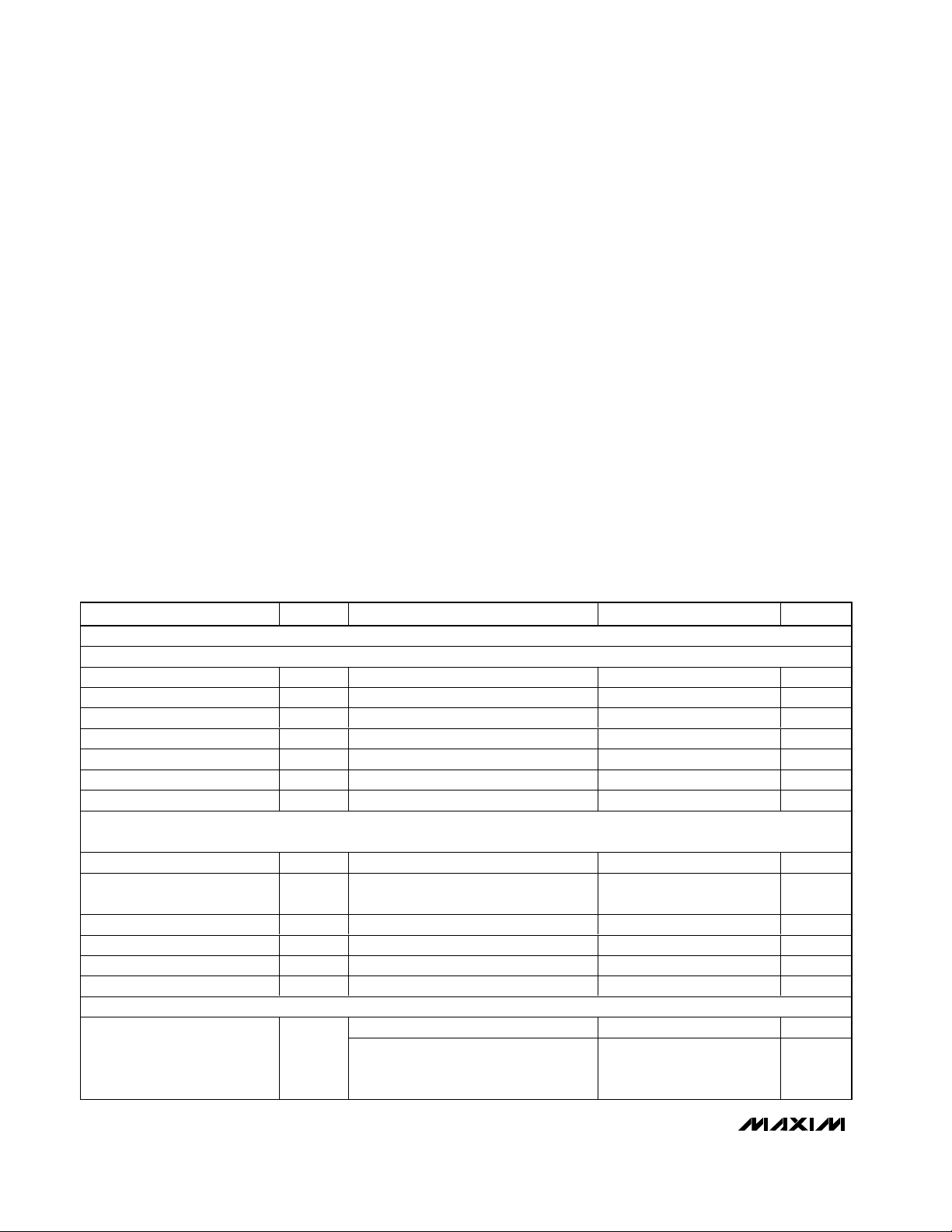
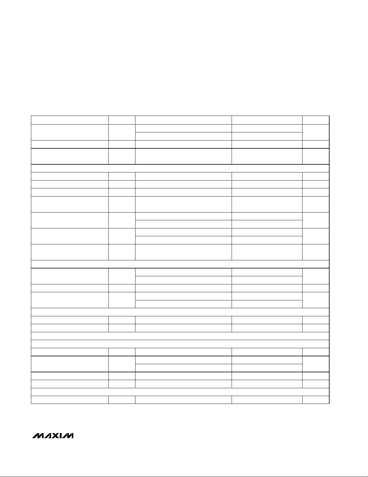
PARAMETER SYMBOL CONDITIONS MIN TYP MAX UNITS
DC ACCURACY (Note 1)
Resolution 10 Bits
Integral Nonlinearity INL ±0.5 ±1.0 LSB
Differential Nonlinearity DNL ±0.5 ±1.0 LSB
Offset Error ±0.25 ±2.0 LSB
Gain Error (Note 2) ±0.025 ±2.0 LSB
Gain Temperature Coefficient ±1.4 ppm/°C
Channel-to-Channel Offset ±0.1 LSB
DYNAMIC SPECIFICATIONS (10kHz sine wave input, VIN = 2.5V
(MAX1020/MAX1022/MAX1058), 300ksps, f
Signal-to-Noise Plus Distortion SINAD 61 dB
Total Harmonic Distortion
(Up to the Fifth Harmonic)
Spurious-Free Dynamic Range SFDR 66 dBc
Intermodulation Distortion IMD f
Full-Linear Bandwidth SINAD > 70dB 100 kHz
Full-Power Bandwidth -3dB point 1 MHz
CONVERSION RATE (Note 3)
Power-Up Time t
ADC
= 4.8MHz)
SCLK
THD -70 dBc
= 9.9kHz, f
in1
External reference 0.8 µs
PU
Internal reference (Note 4) 218
P-P
= 10.2kHz 72 dBc
in2
(MAX1021/MAX1023/MAX1057), VIN = 4.096V
P-P
C onver si on
C l ock
C ycl es
Page 3
MAX1020–MAX1023/MAX1057/MAX1058
10-Bit, Multichannel ADCs/DACs with FIFO,
Temperature Sensing, and GPIO Ports
_______________________________________________________________________________________ 3
ELECTRICAL CHARACTERISTICS (continued)
(AVDD= DVDD= 2.7V to 3.6V (MAX1021/MAX1023/MAX1057), external reference V
REF
= 2.5V (MAX1021/MAX1023/MAX1057), AVDD=
DV
DD
= 4.75V to 5.25V (MAX1020/MAX1022/MAX1058), external reference V
REF
= 4.096V (MAX1020/MAX1022/MAX1058), f
SCLK
= 4.8MHz
(50% duty cycle), T
A
= -40°C to +85°C, unless otherwise noted. Typical values are at AVDD= DVDD= 3V (MAX1021/MAX1023/MAX1057),
AV
DD
= DVDD= 5V (MAX1020/MAX1022/MAX1058), TA= +25°C. Outputs are unloaded, unless otherwise noted.)
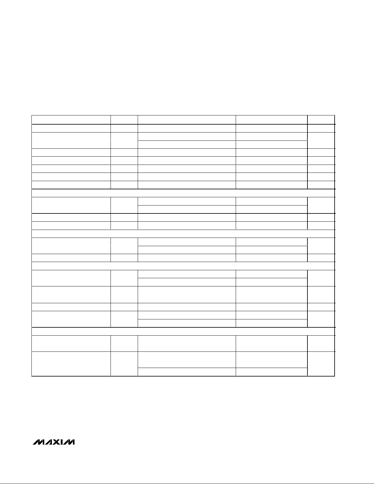
PARAMETER SYMBOL CONDITIONS MIN TYP MAX UNITS
Acquisition Time t
Conversion Time t
Internal Clock Frequency Internally clocked conversion 4.3 MHz
External Clock Frequency f
Duty Cycle 40 60 %
Aperture Delay 30 ns
Aperture Jitter <50 ps
ANALOG INPUTS
Input Voltage Range (Note 6)
Input Leakage Current ±0.01 ±1 µA
Input Capacitance 24 pF
INTERNAL TEMPERATURE SENSOR
Measurement Error (Notes 5, 7)
Temperature Resolution 1/8 °C/LSB
INTERNAL REFERENCE
REF1 Output Voltage (Note 8)
REF1 Voltage Temperature
Coefficient
REF1 Output Impedance 6.5 kΩ
REF1 Short-Circuit Current
EXTERNAL REFERENCE
REF1 Input Voltage Range V
REF2 Input Voltage Range
(Note 4)
ACQ
CONV
CLK
TC
REF1
V
REF2
(Note 5) 0.6 µs
Internally clocked 3.5
Externally clocked 2.7
Externally clocked conversion (Note 5) 0.1 4.8 MHz
Unipolar 0 V
Bipolar -V
TA = +25°C ±0.7
T
= T
A
MAX1021/MAX1023/MAX1057 2.482 2.50 2.518
MAX1020/MAX1022/MAX1058 4.066 4.096 4.126
REF
V
REF
V
REF
REF mode 11 (Note 4) 1
REF mode 01 1
REF mode 11 0 1
to T
MIN
MAX
= 2.5V 0.39
= 4.096V 0.63
/ 2 V
REF
±1.0 ±3.0
±30 ppm/°C
AV
AV
REF
REF
DD
0.05
DD
0.05
/ 2
+
+
µs
V
°C
V
mA
V
V
Page 4
MAX1020–MAX1023/MAX1057/MAX1058
10-Bit, Multichannel ADCs/DACs with FIFO,
Temperature Sensing, and GPIO Ports
4 _______________________________________________________________________________________
ELECTRICAL CHARACTERISTICS (continued)
(AVDD= DVDD= 2.7V to 3.6V (MAX1021/MAX1023/MAX1057), external reference V
REF
= 2.5V (MAX1021/MAX1023/MAX1057), AVDD=
DV
DD
= 4.75V to 5.25V (MAX1020/MAX1022/MAX1058), external reference V
REF
= 4.096V (MAX1020/MAX1022/MAX1058), f
SCLK
= 4.8MHz
(50% duty cycle), T
A
= -40°C to +85°C, unless otherwise noted. Typical values are at AVDD= DVDD= 3V (MAX1021/MAX1023/MAX1057),
AV
DD
= DVDD= 5V (MAX1020/MAX1022/MAX1058), TA= +25°C. Outputs are unloaded, unless otherwise noted.)
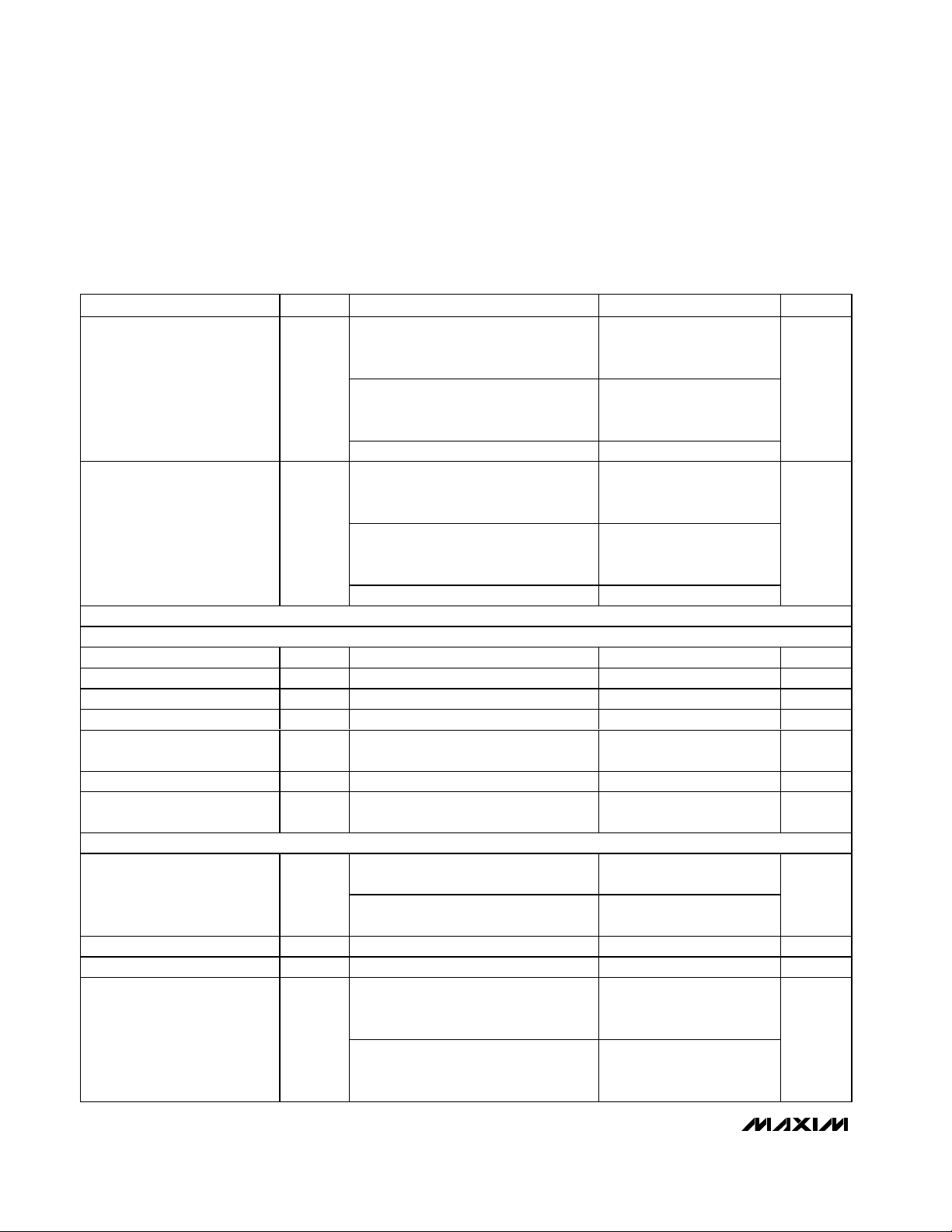
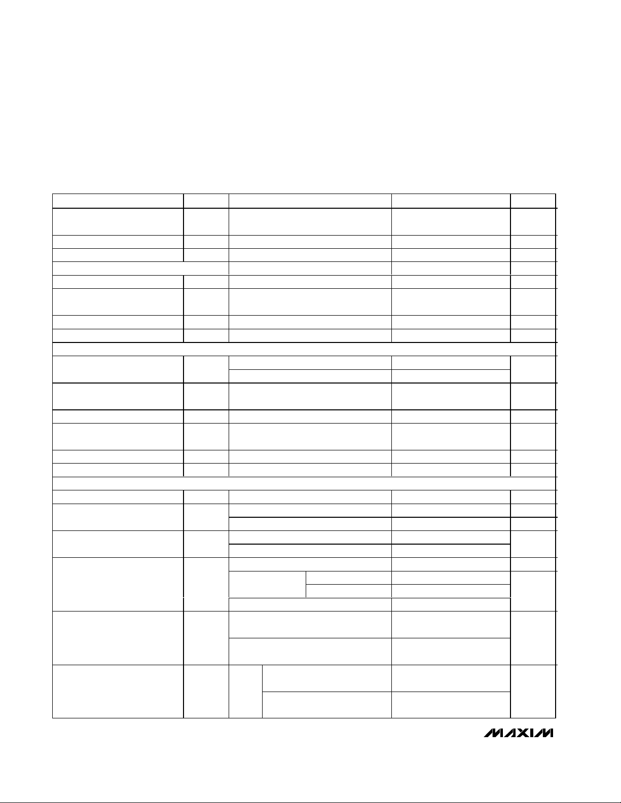
PARAMETER SYMBOL CONDITIONS MIN TYP MAX UNITS
REF1 Input Current (Note 9) I
REF2 Input Current I
DC ACCURACY (Note 10)
Resolution 10 Bits
Integral Nonlinearity INL ±0.5 ±1 LSB
Differential Nonlinearity DNL Guaranteed monotonic ±0.5 LSB
Offset Error V
Offset-Error Drift ±10
Gain Error GE (Note 8) ±1.25 ±10 LSB
Gain Temperature Coefficient ±8
DAC OUTPUT
Output-Voltage Range
DC Output Impedance 0.5 Ω
Capacitive Load (Note 11) 1 nF
Resistive Load to AGND R
V
= 2.5V
REF
(MAX1021/MAX1023/MAX1057),
REF1
REF2
OS
L
f
V
(MAX1020/MAX1022/MAX1058),
f
Acquisition between conversions ±0.01 ±1
V
(MAX1021/MAX1023/MAX1057),
f
V
(MAX1020/MAX1022/MAX1058),
f
Acquisition between conversions ±0.01 ±1
(Note 8) ±3 ±10 mV
No load 0.02
10kΩ load to either rail 0.1
AVDD = 2.7V, V
(MAX1021/MAX1023/MAX1057),
gain error < 1%
AVDD = 4.75V, V
(MAX1020/MAX1022/MAX1058),
gain error < 2%
SAMPLE
= 4.096V
REF
SAMPLE
= 2.5V
REF
SAMPLE
= 4.096V
REF
SAMPLE
= 300ksps
= 300ksps
= 300ksps
= 300ksps
REF
REF
DAC
= 2.5V
= 4.096V
25 80
40 80
25 80
40 80
AV
DD
0.02
AV
DD
0.1
2000
500
-
-
µA
µA
ppm of
FS/°C
ppm of
FS/°C
V
Ω
Page 5
MAX1020–MAX1023/MAX1057/MAX1058
10-Bit, Multichannel ADCs/DACs with FIFO,
Temperature Sensing, and GPIO Ports
_______________________________________________________________________________________ 5
ELECTRICAL CHARACTERISTICS (continued)
(AVDD= DVDD= 2.7V to 3.6V (MAX1021/MAX1023/MAX1057), external reference V
REF
= 2.5V (MAX1021/MAX1023/MAX1057), AVDD=
DV
DD
= 4.75V to 5.25V (MAX1020/MAX1022/MAX1058), external reference V
REF
= 4.096V (MAX1020/MAX1022/MAX1058), f
SCLK
= 4.8MHz
(50% duty cycle), T
A
= -40°C to +85°C, unless otherwise noted. Typical values are at AVDD= DVDD= 3V (MAX1021/MAX1023/MAX1057),
AV
DD
= DVDD= 5V (MAX1020/MAX1022/MAX1058), TA= +25°C. Outputs are unloaded, unless otherwise noted.)
PARAMETER SYMBOL CONDITIONS MIN TYP MAX UNITS
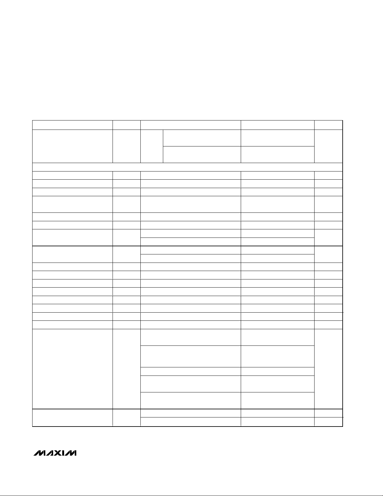
Wake-Up Time (Note 12)
From power-down mode, AVDD = 5V 25
From power-down mode, AV
DD
1kΩ Output Termination Programmed in power-down mode 1 kΩ
100kΩ Output Termination
At wake-up or programmed in
power-down mode
DYNAMIC PERFORMANCE (Notes 5, 13)
Output-Voltage Slew Rate SR Positive and negative 3 V/µs
Output-Voltage Settling Time t
To 1 LSB, 400 - C00 hex (Note 7) 2 5 µs
S
Digital Feedthrough Code 0, all digital inputs from 0 to DV
Major Code Transition Glitch
Impulse
Output Noise (0.1Hz to 50MHz)
Output Noise (0.1Hz to 500kHz)
Between codes 2047 and 2048 4 nV
From V
REF
Using internal reference 720
From V
REF
Using internal reference 320
DAC-to-DAC Transition
Crosstalk
INTERNAL REFERENCE
REF1 Output Voltage (Note 8)
REF1 Temperature Coefficient TC
REF1 Short-Circuit Current
MAX1021/MAX1023/MAX1057 2.482 2.50 2.518
MAX1020/MAX1022/MAX1058 4.066 4.096 4.126
REF
V
= 2.5V 0.39
REF
V
= 4.096V 0.63
REF
EXTERNAL-REFERENCE INPUT
REF1 Input Voltage Range V
REF1 Input Impedance R
REF1
REF1
REF modes 01, 10, and 11 (Note 4) 0.7 AV
DIGITAL INTERFACE
DIGITAL INPUTS (SCLK, DIN, CS, CNVST, LDAC)
Input-Voltage High V
Input-Voltage Low V
Input Leakage Current I
Input Capacitance C
DV
IH
IL
L
IN
= 2.7V to 5.25V 2.4 V
DD
DV
= 3.6V to 5.25V 0.8
DD
DV
= 2.7V to 3.6V 0.6
DD
DIGITAL OUTPUT (DOUT) (Note 14)
Output-Voltage Low V
OL
I
= 2mA 0.4 V
SINK
= 2.7V 21
100 kΩ
DD
0.5 nV•s
660
260
0.5 nV
±30
70 100 130 kΩ
±0.01 ±10 µA
15 pF
DD
µV
µV
ppm/°C
µs
•s
P-P
P-P
•s
V
mA
V
V
Page 6
MAX1020–MAX1023/MAX1057/MAX1058
10-Bit, Multichannel ADCs/DACs with FIFO,
Temperature Sensing, and GPIO Ports
6 _______________________________________________________________________________________
ELECTRICAL CHARACTERISTICS (continued)
(AVDD= DVDD= 2.7V to 3.6V (MAX1021/MAX1023/MAX1057), external reference V
REF
= 2.5V (MAX1021/MAX1023/MAX1057), AVDD=
DV
DD
= 4.75V to 5.25V (MAX1020/MAX1022/MAX1058), external reference V
REF
= 4.096V (MAX1020/MAX1022/MAX1058), f
SCLK
= 4.8MHz
(50% duty cycle), T
A
= -40°C to +85°C, unless otherwise noted. Typical values are at AVDD= DVDD= 3V (MAX1021/MAX1023/MAX1057),
AV
DD
= DVDD= 5V (MAX1020/MAX1022/MAX1058), TA= +25°C. Outputs are unloaded, unless otherwise noted.)
PARAMETER SYMBOL CONDITIONS MIN TYP MAX UNITS
Output-Voltage High V
OHISOURCE
= 2mA
Tri-State Leakage Current ±10 µA
Tri-State Output Capacitance C
OUT
DIGITAL OUTPUT (EOC) (Note 14)
Output-Voltage Low V
Output-Voltage High V
I
OL
OHISOURCE
= 2mA 0.4 V
SINK
= 2mA
Tri-State Leakage Current ±10 µA
Tri-State Output Capacitance C
OUT
DIGITAL OUTPUTS (GPIO_) (Note 14)
I
= 2mA 0.4
GPIOB_, GPIOC_ OutputVoltage Low
GPIOB_, GPIOC_ OutputVoltage High
GPIOA_ Output-Voltage Low I
GPIOA_ Output-Voltage High I
SINK
I
= 4mA 0.8
SINK
I
SOURCE
SINK
SOURCE
= 2mA
= 15mA 0.8 V
= 15mA
Tri-State Leakage Current ±10 µA
Tri-State Output Capacitance C
OUT
POWER REQUIREMENTS (Note 15)
Digital Positive-Supply Voltage DV
Digital Positive-Supply Current DI
Analog Positive-Supply Voltage AV
Analog Positive Supply Current A
DD
Idle, all blocks shut down 0.2 4 µA
DD
Only ADC on, external reference 1 mA
MAX1021/MAX1023/MAX1057 2.7 3.6
DD
MAX1020/MAX1022/MAX1058 4.75 5.25
Idle, all blocks shut down 0.2 1 µA
f
= 300ksps 2.8 4.2
Only ADC on,
IDD
external reference
SAMPLE
= 100ksps 2.6
f
SAMPLE
All DACs on, no load, internal reference 1.5 4.0
AVDD = 2.7V
REF1 Positive-Supply Rejection PSRR
MAX1021/MAX1023/MAX1057
AV
= 4.75V
DD
MAX1020/MAX1022/MAX1058
MAX1021/MAX1023/MAX1057
= 2.7V to 3.6V
AV
DD
M AX 1020/M AX 1022/M AX 1058
= 4.75V to 5.25V
AV
D D
DAC Positive-Supply Rejection PSRD
Output
code =
FFFhex
DV
-
DD
0.5
15 pF
DV
-
DD
0.5
15 pF
DV
-
DD
0.5
DV
-
DD
0.8
15 pF
2.70 AV
-77
-80
±0.1 ±0.5
±0.1 ±0.5
DD
V
V
V
V
V
V
V
mA
dB
mV
Page 7
MAX1020–MAX1023/MAX1057/MAX1058
10-Bit, Multichannel ADCs/DACs with FIFO,
Temperature Sensing, and GPIO Ports
_______________________________________________________________________________________ 7
ELECTRICAL CHARACTERISTICS (continued)
(AVDD= DVDD= 2.7V to 3.6V (MAX1021/MAX1023/MAX1057), external reference V
REF
= 2.5V (MAX1021/MAX1023/MAX1057), AVDD=
DV
DD
= 4.75V to 5.25V (MAX1020/MAX1022/MAX1058), external reference V
REF
= 4.096V (MAX1020/MAX1022/MAX1058), f
SCLK
= 4.8MHz
(50% duty cycle), T
A
= -40°C to +85°C, unless otherwise noted. Typical values are at AVDD= DVDD= 3V (MAX1021/MAX1023/MAX1057),
AV
DD
= DVDD= 5V (MAX1020/MAX1022/MAX1058), TA= +25°C. Outputs are unloaded, unless otherwise noted.)
PARAMETER SYMBOL CONDITIONS MIN TYP MAX UNITS
ADC Positive-Supply Rejection PSRA
Fullscale
input
MAX1021/MAX1023/
MAX1057 AV
M AX 1020/M AX 1022/
M AX 1058 AV
= 2.7V to 3.6V
DD
= 4.75V to 5.25V
D D
TIMING CHARACTERISTICS (Figures 6–13)
SCLK Clock Period t
SCLK Pulse-Width High t
SCLK Pulse-Width Low t
GPIO Output Rise/Fall After
CS Rise
GPIO Input Setup Before CS Fall t
LDAC Pulse Width t
SCLK Fall to DOUT Transition
(Note 16)
SCLK Rise to DOUT Transition
(Notes 16, 17)
CS Fall to SCLK Fall Setup Time t
S C LK Fal l to CS Ri se S etup Ti m et
DIN to SCLK Fall Setup Time t
DIN to SCLK Fall Hold Time t
CS Pulse-Width High t
CS Rise to DOUT Disable t
CS Fall to DOUT Enable t
EOC Fall to CS Fall t
CP
CH
CL
t
GOD
GSU
LDACPWL
t
DOT
t
DOT
CSS
CSH
DS
DH
CSPWH
DOD
DOE
RDS
40/60 duty cycle 16 ns
60/40 duty cycle 16 ns
C
= 20pF 100 ns
LOAD
C
= 20pF, SLOW = 0 1.8 12.0
LOAD
C
= 20pF, SLOW = 1 10 40
LOAD
C
= 20pF, SLOW = 0 1.8 12.0
LOAD
C
= 20pF, SLOW = 1 10 40
LOAD
C
= 20pF 25 ns
LOAD
C
= 20pF 1.5 25.0 ns
LOAD
CKSEL = 01 (temp sense) or CKSEL =
10 (temp sense), internal reference on
CKSEL = 01 (temp sense) or CKSEL =
10 (temp sense), internal reference
initially off
CS or CNVST Rise to EOC Fall t
DOV
CKSEL = 01 (voltage conversion) 8
CKSEL = 10 (voltage conversion),
internal reference on
CKSEL = 10 (voltage conversion),
internal reference initially off
CNVST Pulse Width t
CSW
CKSEL = 00, CKSEL = 01 (temp sense) 40 ns
CKSEL = 01 (voltage conversion) 1.4 µs
40 ns
20 ns
10 ns
10 ns
50 ns
30 ns
±0.06 ±0.5
mV
±0.06 ±0.5
0ns
ns
ns
0ns
0ns
55
120
µs
8
80
Page 8
MAX1020–MAX1023/MAX1057/MAX1058
10-Bit, Multichannel ADCs/DACs with FIFO,
Temperature Sensing, and GPIO Ports
8 _______________________________________________________________________________________
ELECTRICAL CHARACTERISTICS (continued)
(AVDD= DVDD= 2.7V to 3.6V (MAX1021/MAX1023/MAX1057), external reference V
REF
= 2.5V (MAX1021/MAX1023/MAX1057), AVDD=
DV
DD
= 4.75V to 5.25V (MAX1020/MAX1022/MAX1058), external reference V
REF
= 4.096V (MAX1020/MAX1022/MAX1058), f
SCLK
= 4.8MHz
(50% duty cycle), T
A
= -40°C to +85°C, unless otherwise noted. Typical values are at AVDD= DVDD= 3V (MAX1021/MAX1023/MAX1057),
AV
DD
= DVDD= 5V (MAX1020/MAX1022/MAX1058), TA= +25°C. Outputs are unloaded, unless otherwise noted.)
Note 1: Tested at DV
DD
= AVDD= +3.6V (MAX1021/MAX1023/MAX1057), DVDD= AVDD= +5.25V (MAX1020/MAX1022/MAX1058).
Note 2: Offset nulled.
Note 3: No bus activity during conversion. Conversion time is defined as the number of conversion clock cycles multiplied by the
clock period.
Note 4: See Table 5 for reference-mode details.
Note 5: Not production tested. Guaranteed by design.
Note 6: See the ADC/DAC References section.
Note 7: Fast automated test, excludes self-heating effects.
Note 8: Specified over the -40°C to +85°C temperature range.
Note 9: REFSEL[1:0] = 00 or when DACs are not powered up.
Note 10: DAC linearity, gain, and offset measurements are made between codes 115 and 3981.
Note 11: The DAC buffers are guaranteed by design to be stable with a 500pF load.
Note 12: Time required by the DAC output to power up and settle within 1 LSB in the external reference mode.
Note 13: All DAC dynamic specifications are valid for a load of 1nF and 10kΩ.
Note 14: Only one digital output (either DOUT, EOC, or the GPIOs) can be indefinitely shorted to either supply at one time.
Note 15: All digital inputs at either DV
DD
or DGND. DVDDshould not exceed AVDD.
Note 16: See the Reset Register section and Table 9 for details on programming the SLOW bit.
Note 17: Clock mode 11 only.
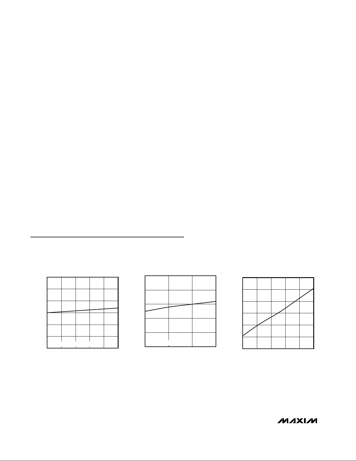
SHUTDOWN CURRENT
vs. ANALOG SUPPLY VOLTAGE
MAX1020 toc01
SUPPLY VOLTAGE (V)
SHUTDOWN CURRENT (µA)
5.155.054.954.85
0.05
0.10
0.15
0.20
0.25
0.30
0
4.75 5.25
MAX1020/MAX1022/MAX1058
SHUTDOWN CURRENT
vs. ANALOG SUPPLY VOLTAGE
MAX1020 toc02
SUPPLY VOLTAGE (V)
SHUTDOWN CURRENT (µA)
3.33.0
0.12
0.14
0.16
0.18
0.20
0.10
2.7 3.6
MAX1021/MAX1023/MAX1057
SHUTDOWN CURRENT
vs. TEMPERATURE
MAX1020 toc03
TEMPERATURE (°C)
SHUTDOWN CURRENT (µA)
603510-15
0.1
0.2
0.3
0.4
0.5
0.6
0
-40 85
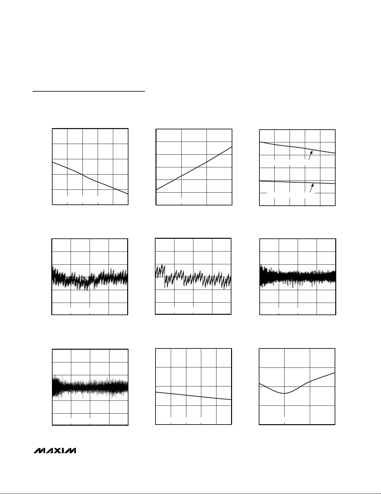
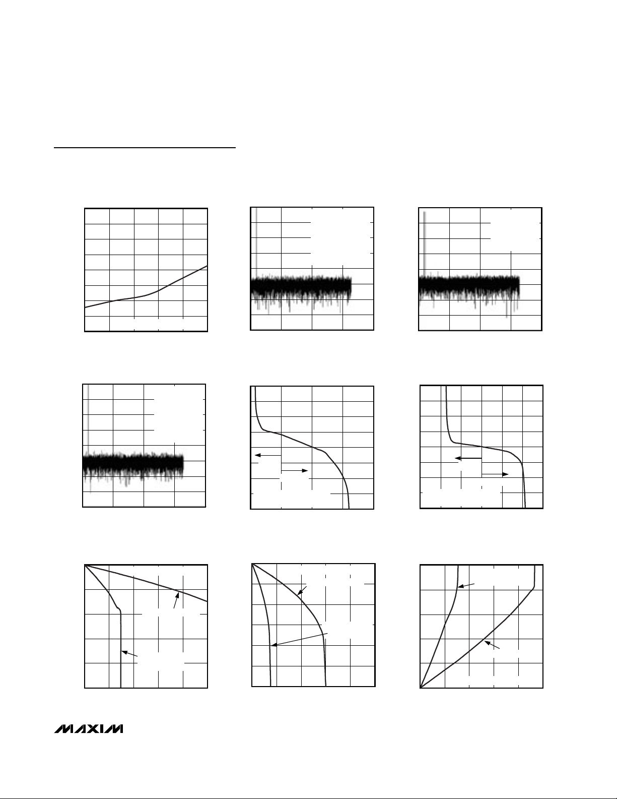
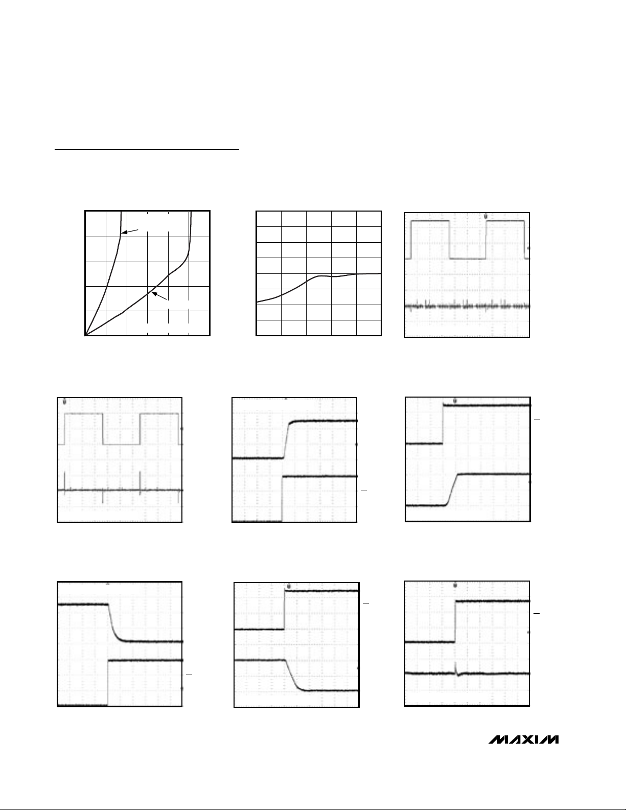
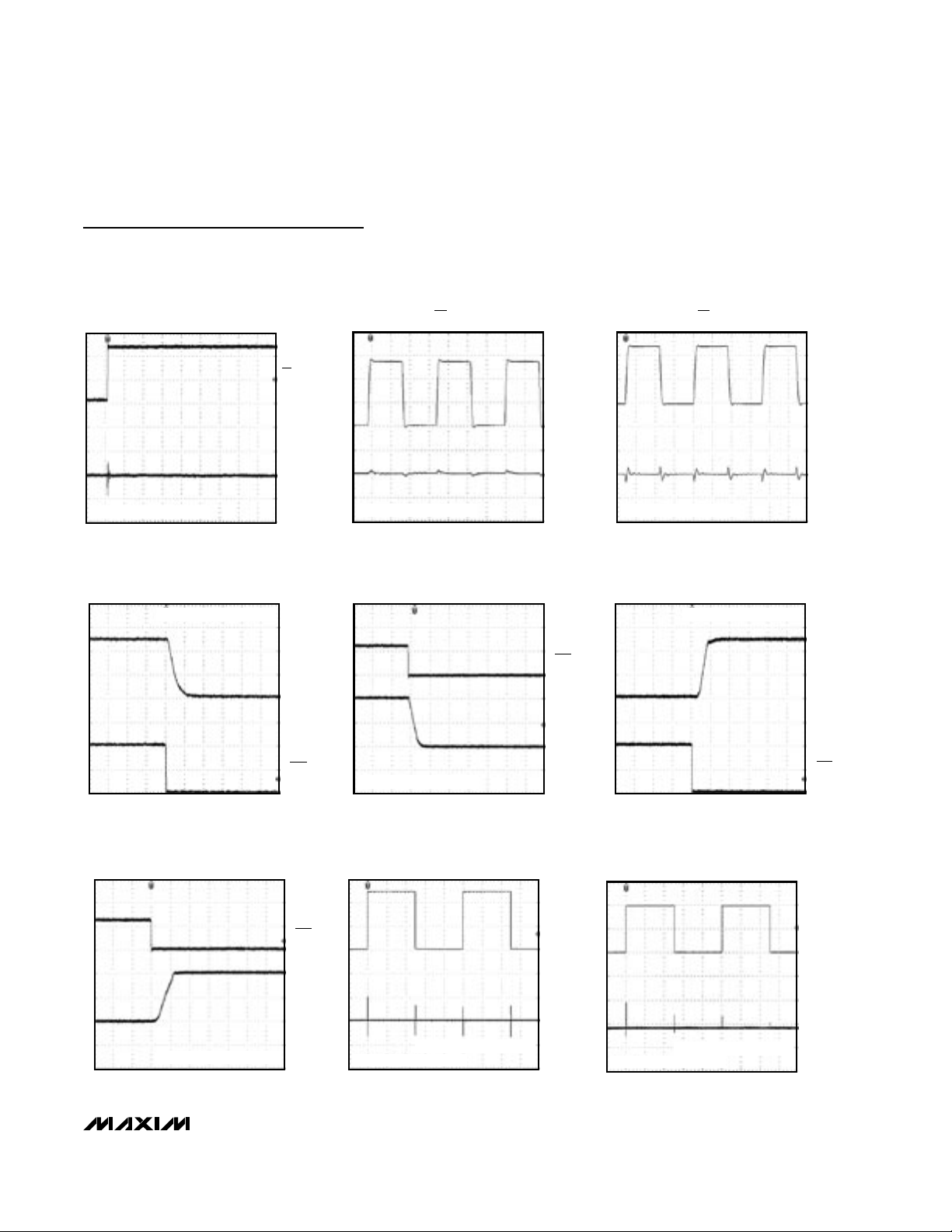
Typical Operating Characteristics
(AVDD= DVDD= 3V (MAX1021/MAX1023/MAX1057), external V
REF
= 2.5V (MAX1021/MAX1023/MAX1057), AVDD= DVDD= 5V
(MAX1020/MAX1022/MAX1058), external V
REF
= 4.096V (MAX1020/MAX1022/MAX1058), f
CLK
= 4.8MHz (50% duty cycle), f
SAMPLE
= 300ksps, C
LOAD
= 50pF, 0.1µF capacitor at REF, TA= +25°C, unless otherwise noted.)
Page 9
MAX1020–MAX1023/MAX1057/MAX1058
10-Bit, Multichannel ADCs/DACs with FIFO,
Temperature Sensing, and GPIO Ports
_______________________________________________________________________________________ 9
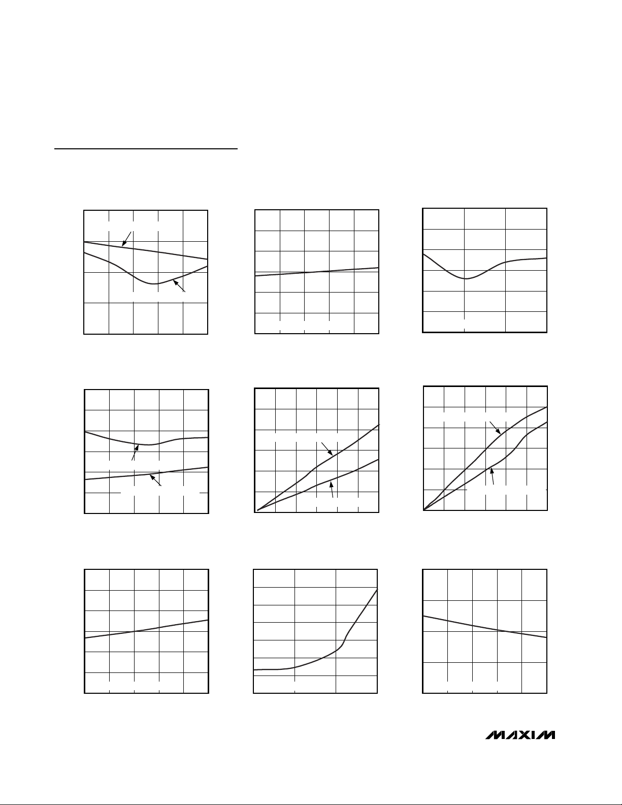
Typical Operating Characteristics (continued)
(AVDD= DVDD= 3V (MAX1021/MAX1023/MAX1057), external V
REF
= 2.5V (MAX1021/MAX1023/MAX1057), AVDD= DVDD= 5V
(MAX1020/MAX1022/MAX1058), external V
REF
= 4.096V (MAX1020/MAX1022/MAX1058), f
CLK
= 4.8MHz (50% duty cycle), f
SAMPLE
= 300ksps, C
LOAD
= 50pF, 0.1µF capacitor at REF, TA= +25°C, unless otherwise noted.)
INTERNAL OSCILLATOR FREQUENCY
4.5
4.4
4.3
4.2
4.1
INTERNAL OSCILLATOR FREQUENCY (MHz)
MAX1020/MAX1022/MAX1058
4.0
4.75 5.25
vs. ANALOG SUPPLY VOLTAGE
SUPPLY VOLTAGE (V)
5.155.054.954.85
ADC INTEGRAL NONLINEARITY
vs. OUTPUT CODE
0.3
0.2
0.1
INTERNAL OSCILLATOR FREQUENCY
vs. ANALOG SUPPLY VOLTAGE
4.90
4.85
MAX1020 toc04
4.80
4.75
4.70
4.65
INTERNAL OSCILLATOR FREQUENCY (MHz)
MAX1021/MAX1023/MAX1057
4.60
2.7 3.6
ADC INTEGRAL NONLINEARITY
vs. OUTPUT CODE
0.3
0.2
MAX1020 toc07
0.1
INTERNAL OSCILLATOR FREQUENCY
vs. TEMPERATURE
5.0
4.8
MAX1020 toc05
4.6
MAX1021/MAX1023/MAX1057
4.4
4.2
4.0
INTERNAL OSCILLATOR FREQUENCY (MHz)
3.33.0
SUPPLY VOLTAGE (V)
MAX1020/MAX1022/MAX1058
3.8
-40 85
TEMPERATURE (°C)
ADC DIFFERENTIAL NONLINEARITY
vs. OUTPUT CODE
0.3
0.2
MAX1020 toc08
0.1
MAX1020 toc06
603510-15
MAX1020 toc09
0
-0.1
INTEGRAL NONLINEARITY (LSB)
-0.2
MAX1020/MAX1022/MAX1058
-0.3
0 1024
OUTPUT CODE
ADC DIFFERENTIAL NONLINEARITY
vs. OUTPUT CODE
0.3
0.2
0.1
0
-0.1
DIFFERENTIAL NONLINEARITY (LSB)
-0.2
MAX1021/MAX1023/MAX1057
-0.3
0 1024
OUTPUT CODE
0
-0.1
INTEGRAL NONLINEARITY (LSB)
-0.2
MAX1021/MAX1023/MAX1057
-0.3
768512256
0 1024
OUTPUT CODE
768512256
ADC OFFSET ERROR
vs. ANALOG SUPPLY VOLTAGE
-0.4
MAX1020 toc10
-0.5
-0.6
OFFSET ERROR (LSB)
-0.7
MAX1020/MAX1022/MAX1058
-0.8
768512256
4.75 5.25
SUPPLY VOLTAGE (V)
5.155.054.954.85
MAX1020 toc11
0
-0.1
DIFFERENTIAL NONLINEARITY (LSB)
-0.2
MAX1020/MAX1022/MAX1058
-0.3
0 1024
OUTPUT CODE
ADC OFFSET ERROR
vs. ANALOG SUPPLY VOLTAGE
0
-0.5
-1.0
OFFSET ERROR (LSB)
-1.5
MAX1021/MAX1023/MAX1057
-2.0
2.7 3.6
SUPPLY VOLTAGE (V)
3.33.0
768512256
MAX1020 toc12
Page 10
MAX1020–MAX1023/MAX1057/MAX1058
10-Bit, Multichannel ADCs/DACs with FIFO,
Temperature Sensing, and GPIO Ports
10 ______________________________________________________________________________________
Typical Operating Characteristics (continued)
(AVDD= DVDD= 3V (MAX1021/MAX1023/MAX1057), external V
REF
= 2.5V (MAX1021/MAX1023/MAX1057), AVDD= DVDD= 5V
(MAX1020/MAX1022/MAX1058), external V
REF
= 4.096V (MAX1020/MAX1022/MAX1058), f
CLK
= 4.8MHz (50% duty cycle), f
SAMPLE
= 300ksps, C
LOAD
= 50pF, 0.1µF capacitor at REF, TA= +25°C, unless otherwise noted.)
ADC OFFSET ERROR
vs. TEMPERATURE
0
MAX1020/MAX1022/MAX1058
-0.5
-1.0
OFFSET ERROR (LSB)
-1.5
-2.0
-40 85
MAX1021/MAX1023/MAX1057
603510-15
TEMPERATURE (°C)
ADC GAIN ERROR
vs. TEMPERATURE
1.00
vs. ANALOG SUPPLY VOLTAGE
0.050
MAX1020 toc13
0.025
0
-0.025
GAIN ERROR (LSB)
-0.050
MAX1020/MAX1022/MAX1058
-0.075
4.75 5.25
ADC EXTERNAL REFERENCE
INPUT CURRENT vs. SAMPLING RATE
60
ADC GAIN ERROR
ADC GAIN ERROR
vs. ANALOG SUPPLY VOLTAGE
0.50
0.45
MAX1020 toc14
0.40
0.35
GAIN ERROR (LSB)
0.30
0.25
MAX1021/MAX1023/MAX1057
0.20
5.155.054.954.85
SUPPLY VOLTAGE (V)
2.7 3.6
SUPPLY VOLTAGE (V)
ANALOG SUPPLY CURRENT
vs. SAMPLING RATE
3.0
MAX1020 toc15
3.33.0
0.75
0.50
0.25
MAX1021/MAX1023/MAX1057
GAIN ERROR (LSB)
0
-0.25
-0.50
-40 85
MAX1020/MAX1022/MAX1058
603510-15
TEMPERATURE (°C)
ANALOG SUPPLY CURRENT
vs. ANALOG SUPPLY VOLTAGE
2.8
2.7
2.6
2.5
2.4
SUPPLY CURRENT (mA)
2.3
MAX1020/MAX1022/MAX1058
2.2
4.75 5.25
SUPPLY VOLTAGE (V)
5.155.054.954.85
50
MAX1020 toc16
40
30
20
10
ADC EXTERNAL REFERENCE INPUT CURRENT (µA)
0
2.6
2.5
MAX1020 toc19
2.4
2.3
2.2
SUPPLY CURRENT (mA)
2.1
2.0
1.9
MAX1020/MAX1022/MAX1058
MAX1021/MAX1023/MAX1057
0 300
SAMPLING RATE (ksps)
25020015010050
ANALOG SUPPLY CURRENT
vs. ANALOG SUPPLY VOLTAGE
MAX1021/MAX1023/MAX1057
2.7 3.6
SUPPLY VOLTAGE (V)
3.33.0
2.5
MAX1020 toc17
2.0
1.5
1.0
ANALOG SUPPLY CURRENT (mA)
0.5
0
0 300
2.7
MAx1020 toc20
2.6
2.5
2.4
ANALOG SUPPLY CURRENT (mA)
MAX1020/MAX1022/MAX1058
2.3
-40 85
MAX1020/MAX1022/MAX1058
ANALOG SUPPLY CURRENT
MAX1020 toc18
MAX1021/MAX1023/MAX1057
25020015010050
SAMPLING RATE (ksps)
vs. TEMPERATURE
MAX1020 toc21
603510-15
TEMPERATURE (°C)
Page 11
MAX1020–MAX1023/MAX1057/MAX1058
10-Bit, Multichannel ADCs/DACs with FIFO,
Temperature Sensing, and GPIO Ports
______________________________________________________________________________________ 11
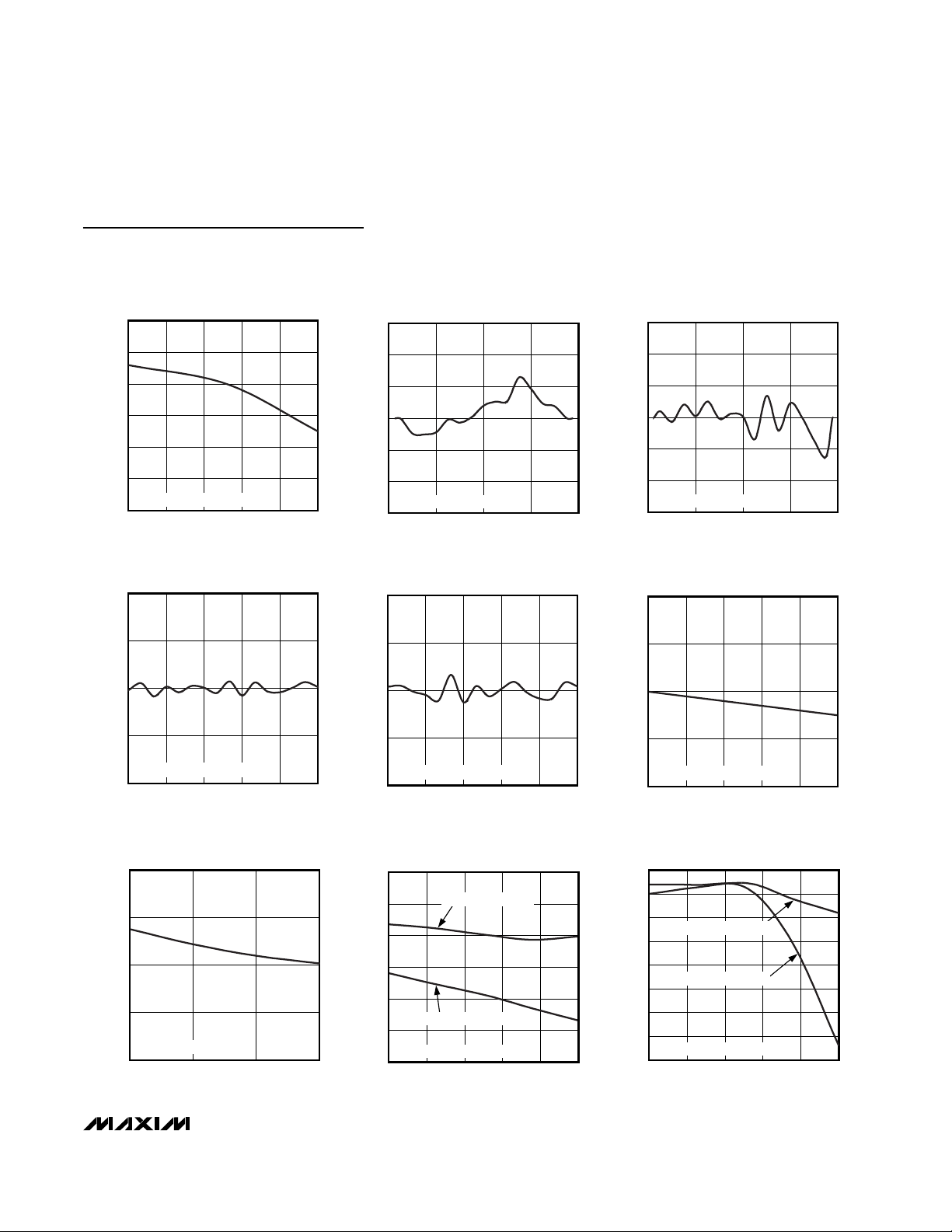
Typical Operating Characteristics (continued)
(AVDD= DVDD= 3V (MAX1021/MAX1023/MAX1057), external V
REF
= 2.5V (MAX1021/MAX1023/MAX1057), AVDD= DVDD= 5V
(MAX1020/MAX1022/MAX1058), external V
REF
= 4.096V (MAX1020/MAX1022/MAX1058), f
CLK
= 4.8MHz (50% duty cycle), f
SAMPLE
= 300ksps, C
LOAD
= 50pF, 0.1µF capacitor at REF, TA= +25°C, unless otherwise noted.)
2.16
2.15
2.14
2.13
2.12
ANALOG SUPPLY CURRENT (mA)
2.11
2.10
ANALOG SUPPLY CURRENT
vs. TEMPERATURE
MAX1021/MAX1023/MAX1057
-40 85
TEMPERATURE (°C)
603510-15
DAC DIFFERENTIAL NONLINEARITY
vs. OUTPUT CODE
0.10
0.05
DAC INTEGRAL NONLINEARITY
0.3
0.2
MAX1020 toc22
0.1
0
-0.1
INTEGRAL NONLINEARITY (LSB)
-0.2
MAX1020/MAX1022/MAX1058
-0.3
0 1024
DAC DIFFERENTIAL NONLINEARITY
vs. OUTPUT CODE
0.10
MAX1020 toc25
0.05
DAC INTEGRAL NONLINEARITY
vs. OUTPUT CODE
OUTPUT CODE
0.3
0.2
MAX1020 toc23
0.1
0
-0.1
INTEGRAL NONLINEARITY (LSB)
-0.2
MAX1021/MAX1023/MAX1057
-0.3
768512256
0 1024
vs. OUTPUT CODE
OUTPUT CODE
DAC FULL-SCALE ERROR
vs. ANALOG SUPPLY VOLTAGE
0.04
MAX1020 toc26
0.03
MAX1020 toc24
768512256
MAX1020 toc27
0
-0.05
DIFFERENTIAL NONLINEARITY (LSB)
MAX1020/MAX1022/MAX1058
-0.10
1023 1038
OUTPUT CODE
DAC FULL-SCALE ERROR
vs. ANALOG SUPPLY VOLTAGE
-0.50
-0.55
-0.60
-0.65
DAC FULL-SCALE ERROR (LSB)
MAX1021/MAX1023/MAX1057
-0.70
2.7 3.6
SUPPLY VOLTAGE (V)
3.33.0
0
-0.05
DIFFERENTIAL NONLINEARITY (LSB)
MAX1021/MAX1023/MAX1057
1035103210291026
-0.10
1023 1038
OUTPUT CODE
1035103210291026
DAC FULL-SCALE ERROR
vs. TEMPERATURE
2.0
1.5
MAx1020 toc28
1.0
0.5
0
DAC FULL-SCALE ERROR (LSB)
-0.5
MAX1020/MAX1022/MAX1058
-1.0
-40 85
INTERNAL REFERENCE
EXTERNAL REFERENCE = 4.096V
603510-15
TEMPERATURE (°C)
0.02
0.01
DAC FULL-SCALE ERROR (LSB)
MAX1020/MAX1022/MAX1058
0
4.75 5.25
0
-0.25
MAX1020 toc29
-0.50
EXTERNAL REFERENCE = 2.500V
-0.75
-1.00
-1.25
-1.50
DAC FULL-SCALE ERROR (LSB)
-1.75
MAX1021/MAX1023/MAX1057
-2.00
-40 85
5.155.054.954.85
SUPPLY VOLTAGE (V)
DAC FULL-SCALE ERROR
vs. TEMPERATURE
MAX1020 toc30
INTERNAL REFERENCE
603510-15
TEMPERATURE (°C)
Page 12
MAX1020–MAX1023/MAX1057/MAX1058
10-Bit, Multichannel ADCs/DACs with FIFO,
Temperature Sensing, and GPIO Ports
12 ______________________________________________________________________________________
Typical Operating Characteristics (continued)
(AVDD= DVDD= 3V (MAX1021/MAX1023/MAX1057), external V
REF
= 2.5V (MAX1021/MAX1023/MAX1057), AVDD= DVDD= 5V
(MAX1020/MAX1022/MAX1058), external V
REF
= 4.096V (MAX1020/MAX1022/MAX1058), f
CLK
= 4.8MHz (50% duty cycle), f
SAMPLE
= 300ksps, C
LOAD
= 50pF, 0.1µF capacitor at REF, TA= +25°C, unless otherwise noted.)
1.00
0.75
0.50
0.25
0
-0.25
-0.50
DAC FULL-SCALE ERROR (LSB)
-0.75
-1.00
DAC FULL-SCALE ERROR
vs. REFERENCE VOLTAGE
MAX1020/MAX1022/MAX1058
05
REFERENCE VOLTAGE (V)
431 2
DAC FULL-SCALE ERROR
DAC FULL-SCALE ERROR
vs. REFERENCE VOLTAGE
0
-0.5
MAX1020 toc31
-1.0
-1.5
-2.0
DAC FULL-SCALE ERROR (LSB)
-2.5
MAX1021/MAX1023/MAX1057
-3.0
0 3.0
INTERNAL REFERENCE VOLTAGE
vs. LOAD CURRENT
1
4.12
DAC FULL-SCALE ERROR
vs. LOAD CURRENT
1
MAX1020 toc32
0
-1
-2
DAC FULL-SCALE ERROR (LSB)
-3
MAX1020/MAX1022/MAX1058
2.0 2.51.50.5 1.0
REFERENCE VOLTAGE (V)
-4
030
LOAD CURRENT (mA)
INTERNAL REFERENCE VOLTAGE
vs. TEMPERATURE
2.52
vs. TEMPERATURE
MAX1020 toc33
252015105
0
-1
-2
DAC FULL-SCALE ERROR (LSB)
-3
MAX1021/MAX1023/MAX1057
-4
0 3.0
LOAD CURRENT (mA)
ADC REFERENCE SUPPLY CURRENT
vs. ANALOG SUPPLY VOLTAGE
43.0
42.8
42.6
42.4
42.2
ADC REFERENCE SUPPLY CURRENT (µA)
MAX1020/MAX1022/MAX1058
42.0
4.75 5.25
SUPPLY VOLTAGE (V)
5.155.054.954.85
MAX1020 toc34
4.11
4.10
4.09
INTERNAL REFERENCE VOLTAGE (V)
MAX1020/MAX1022/MAX1058
2.52.01.51.00.5
4.08
-40 85
TEMPERATURE (°C)
603510-15
ADC REFERENCE SUPPLY CURRENT
vs. ANALOG SUPPLY VOLTAGE
25.8
MAX1020 toc37
25.7
25.6
25.5
ADC REFERENCE SUPPLY CURRENT (µA)
MAX1021/MAX1023/MAX1057
25.4
2.7 3.6
SUPPLY VOLTAGE (V)
3.33.0
MAX1020 toc35
2.51
2.50
2.49
INTERNAL REFERENCE VOLTAGE (V)
MAX1021/MAX1023/MAX1057
2.48
-40 85
ADC REFERENCE SUPPLY CURRENT
50
MAX1020 toc38
48
46
44
42
ADC REFERENCE SUPPLY CURRENT (µA)
40
-40 85
MAX1020 toc36
603510-15
TEMPERATURE (°C)
vs. TEMPERATURE
MAX1020 toc39
MAX1020/MAX1022/MAX1058
603510-15
TEMPERATURE (°C)
Page 13
MAX1020–MAX1023/MAX1057/MAX1058
10-Bit, Multichannel ADCs/DACs with FIFO,
Temperature Sensing, and GPIO Ports
______________________________________________________________________________________ 13
Typical Operating Characteristics (continued)
(AVDD= DVDD= 3V (MAX1021/MAX1023/MAX1057), external V
REF
= 2.5V (MAX1021/MAX1023/MAX1057), AVDD= DVDD= 5V
(MAX1020/MAX1022/MAX1058), external V
REF
= 4.096V (MAX1020/MAX1022/MAX1058), f
CLK
= 4.8MHz (50% duty cycle), f
SAMPLE
= 300ksps, C
LOAD
= 50pF, 0.1µF capacitor at REF, TA= +25°C, unless otherwise noted.)
ADC REFERENCE SUPPLY CURRENT
27.00
26.75
26.50
26.25
26.00
25.75
25.50
25.25
ADC REFERENCE SUPPLY CURRENT (µA)
25.00
-40 85
vs. TEMPERATURE
MAX1021/MAX1023/MAX1057
TEMPERATURE (°C)
6035-15 10
ADC CROSSTALK PLOT
0
-20
-40
-60
-80
-100
AMPLITUDE (dB)
-120
-140
-160
0 200
ANALOG INPUT FREQUENCY (kHz)
f
= 5.24288MHz
CLK
= 10.080kHz
f
IN1
= 8.0801kHz
f
IN2
SNR = 61.11dBc
THD = 73.32dBc
ENOB = 9.86 BITS
SFDR = 86.34dBc
15010050
GPIO OUTPUT VOLTAGE
vs. SOURCE CURRENT
5
4
3
2
GPIO OUTPUT VOLTAGE (V)
1
0
0 100
MAX1020/MAX1022/MAX1058
GPIOA0–A3 OUTPUTS
GPIOB0–B3,
C0–C3 OUTPUTS
SOURCE CURRENT (mA)
80604020
0
-20
MAX1020 toc40
-40
-60
-80
-100
AMPLITUDE (dB)
-120
-140
-160
0 200
ANALOG INPUT FREQUENCY (kHz)
DAC OUTPUT LOAD REGULATION
vs. OUTPUT CURRENT
2.08
2.07
MAX1020 toc43
2.06
2.05
2.04
2.03
SINKING
DAC OUTPUT VOLTAGE (V)
2.02
2.01
2.00
-30 90
SOURCING
DAC OUTPUT = MIDSCALE
MAX1020/MAX1022/MAX1058
OUTPUT CURRENT (mA)
GPIO OUTPUT VOLTAGE
vs. SOURCE CURRENT
3.0
2.5
MAX1020 toc46
2.0
1.5
1.0
GPIO OUTPUT VOLTAGE (V)
0.5
0
0 100
SOURCE CURRENT (mA)
ADC FFT PLOT
f
SAMPLE
f
ANALOG_)N
= 5.24288MHz
f
CLK
SINAD = 61.21dBc
SNR = 61.21dBc
THD = 73.32dBc
SFDR = 81.25dBc
= 32.768kHz
= 10.080kHz
15010050
MAX1020 toc41
ADC IMD PLOT
0
-20
-40
-60
-80
-100
AMPLITUDE (dB)
-120
-140
-160
0 200
ANALOG INPUT FREQUENCY (kHz)
DAC OUTPUT LOAD REGULATION
vs. OUTPUT CURRENT
1.29
1.28
MAX1020 toc44
1.27
1.26
1.25
1.24
DAC OUTPUT VOLTAGE (V)
1.23
1.22
DAC OUTPUT = MIDSCALE
MAX1021/MAX1023/MAX1057
1.21
60300
-30 30
SINKING
SOURCING
-10
OUTPUT CURRENT (mA)
GPIO OUTPUT VOLTAGE
vs. SINK CURRENT
MAX1021/MAX1023/MAX1057
GPIOA0–A3 OUTPUTS
GPIOB0–B3, C0–C3
OUTPUTS
80604020
1500
MAX1020 toc47
1200
900
600
GPIO OUTPUT VOLTAGE (mV)
300
0
0 100
GPIOB0–B3, C0–C3
GPIOA0–A3 OUTPUTS
MAX1020/MAX1022/MAX1058
SINK CURRENT (mA)
f
= 5.24288MHz
CLK
= 9.0kHz
f
IN1
= 11.0kHz
f
IN2
= -6dBFS
A
IN
IMD = 78.0dBc
15010050
OUTPUTS
MAX1020 toc42
MAX1020 toc45
20100-20
MAX1020 toc48
80604020
Page 14
MAX1020–MAX1023/MAX1057/MAX1058
10-Bit, Multichannel ADCs/DACs with FIFO,
Temperature Sensing, and GPIO Ports
14 ______________________________________________________________________________________
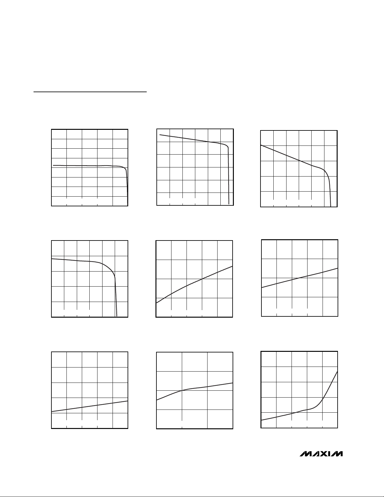
Typical Operating Characteristics (continued)
(AVDD= DVDD= 3V (MAX1021/MAX1023/MAX1057), external V
REF
= 2.5V (MAX1021/MAX1023/MAX1057), AVDD= DVDD= 5V
(MAX1020/MAX1022/MAX1058), external V
REF
= 4.096V (MAX1020/MAX1022/MAX1058), f
CLK
= 4.8MHz (50% duty cycle), f
SAMPLE
= 300ksps, C
LOAD
= 50pF, 0.1µF capacitor at REF, TA= +25°C, unless otherwise noted.)
1500
1200
900
600
GPIO OUTPUT VOLTAGE (mV)
300
0
GPIO OUTPUT VOLTAGE
vs. SINK CURRENT
GPIOB0–B3, C0–C3
OUTPUTS
GPIOA0–A3 OUTPUTS
MAX1021/MAX1023/MAX1057
060
SINK CURRENT (mA)
40 50302010
TEMPERATURE SENSOR ERROR
1.00
0.75
MAX1020 toc49
0.50
0.25
0
-0.25
-0.50
TEMPERATURE SENSOR ERROR (°C)
-0.75
-1.00
-40 85
DAC-TO-DAC CROSSTALK
vs. TEMPERATURE
MAX1020 toc50
6035-15 10
TEMPERATURE (°C)
= 10kΩ, C
R
LOAD
MAX1021/MAX1023/MAX1057
LOAD
100µs
= 100pF
MAX1020 toc51
V
OUTA
1V/div
V
OUTB
10mV/div
AC-COUPLED
DAC-TO-DAC CROSSTALK
= 10kΩ, C
R
LOAD
MAX1020/MAX1022/MAX1058
100µs
LOAD
= 100pF
MAX1020 toc52
V
OUTA
2V/div
V
OUTB
10mV/div
AC-COUPLED
DYNAMIC RESPONSE FALL TIME
= 10kΩ, C
R
LOAD
MAX1021/MAX1023/MAX1057
1µs
LOAD
= 100pF
MAX1020 toc55
V
OUT
1V/div
CS
1V/div
DYNAMIC RESPONSE RISE TIME
= 10kΩ, C
R
LOAD
MAX1021/MAX1023/MAX1057
1µs
LOAD
= 100pF
DYNAMIC RESPONSE FALL TIME
= 10kΩ, C
R
LOAD
MAX1020/MAX1022/MAX1058
1µs
LOAD
= 100pF
MAX1020 toc53
MAX1020 toc56
V
OUT
1V/div
CS
1V/div
CS
2V/div
V
OUT
2V/div
DYNAMIC RESPONSE RISE TIME
= 10kΩ, C
R
LOAD
MAX1020/MAX1022/MAX1058
MAJOR CARRY TRANSITION
= 10kΩ, C
R
LOAD
MAX1021/MAX1023/MAX1057
1µs
1µs
LOAD
LOAD
= 100pF
MAX1020 toc54
= 100pF
MAX1020 toc57
CS
2V/div
V
OUT
2V/div
CS
1V/div
V
OUT
10mV/div
AC-COUPLED
Page 15
MAX1020–MAX1023/MAX1057/MAX1058
10-Bit, Multichannel ADCs/DACs with FIFO,
Temperature Sensing, and GPIO Ports
______________________________________________________________________________________ 15
Typical Operating Characteristics (continued)
(AVDD= DVDD= 3V (MAX1021/MAX1023/MAX1057), external V
REF
= 2.5V (MAX1021/MAX1023/MAX1057), AVDD= DVDD= 5V
(MAX1020/MAX1022/MAX1058), external V
REF
= 4.096V (MAX1020/MAX1022/MAX1058), f
CLK
= 4.8MHz (50% duty cycle), f
SAMPLE
= 300ksps, C
LOAD
= 50pF, 0.1µF capacitor at REF, TA= +25°C, unless otherwise noted.)
MAJOR CARRY TRANSITION
= 10kΩ, C
R
LOAD
MAX1020/MAX1022/MAX1058
= 100pF
LOAD
1µs
MAX1020 toc58
CS
2V/div
V
OUT
20mV/div
AC-COUPLED
NEGATIVE FULL-SCALE SETTLING TIME
R
LOAD
= 10kΩ, C
MAX1021/MAX1023/MAX1057
LOAD
= 100pF
MAX1020 toc61
V
OUT
1V/div
DAC DIGITAL FEEDTHROUGH (R
= 100pF, CS = HIGH, DIN = LOW)
C
LOAD
MAX1021/MAX1023/MAX1057
200ns
NEGATIVE FULL-SCALE SETTLING TIME
= 10kΩ, C
R
LOAD
LOAD
= 10kΩ,
MAX1020 toc59
SCLK
1V/div
V
OUT
100mV/div
AC-COUPLED
DAC DIGITAL FEEDTHROUGH (R
= 100pF, CS = HIGH, DIN = LOW)
C
LOAD
MAX1020/MAX1022/MAX1058
200ns
LOAD
POSITIVE FULL-SCALE SETTLING TIME
LOAD
= 100pF
MAX1020 toc62
V
LDAC
2V/div
R
LOAD
= 10kΩ, C
MAX1021/MAX1023/MAX1057
LOAD
= 100pF
= 10kΩ,
MAX1020 toc60
MAX1020 toc63
SCLK
2V/div
V
OUT
100mV/div
AC-COUPLED
V
OUT_
1V/div
1µs
POSITIVE FULL-SCALE SETTLING TIME
R
LOAD
= 10kΩ, C
MAX1020/MAX1022/MAX1058
1µs
LOAD
= 100pF
MAX1020 toc64
V
LDAC
1V/div
V
LDAC
2V/div
V
OUT_
2V/div
MAX1020/MAX1022/MAX1058
2µs
ADC REFERENCE FEEDTHROUGH
= 10kΩ, C
R
LOAD
ADC REFERENCE SWITCHING
MAX1021/MAX1023/MAX1057
200µs
LOAD
= 100pF
MAX1020 toc65
V
OUT_
2V/div
V
REF2
1V/div
V
DAC-OUT
10mV/div
AC-COUPLED
1µs
ADC REFERENCE FEEDTHROUGH
= 10kΩ, C
R
LOAD
ADC REFERENCE SWITCHING
MAX1020/MAX1022/MAX1058
200µs
LOAD
= 100pF
MAX1020 toc66
V
LDAC
1V/div
V
REF2
2V/div
V
DAC-OUT
2mV/div
AC-COUPLED
Page 16

MAX1020–MAX1023/MAX1057/MAX1058
10-Bit, Multichannel ADCs/DACs with FIFO,
Temperature Sensing, and GPIO Ports
16 ______________________________________________________________________________________
Pin Description
MAX1020/
MAX1021
MAX1022/
MAX1057/
NAME FUNCTION
1, 2 — —
General-Purpose I/O A0, A1. GPIOA0, A1 can sink and source 15mA.
334 EOC
Active-Low End-of-Conversion Output. Data is valid after the falling edge
of EOC.
447 DV
DD
Digital Positive-Power Input. Bypass DVDD to DGND with a 0.1µF
capacitor.
558 DGND Digital Ground. Connect DGND to AGND.
669 DOUT
Serial-Data Output. Data is clocked out on the falling edge of the SCLK
clock in modes 00, 01, and 10. Data is clocked out on the rising edge of
the SCLK clock in mode 11. It is high impedance when CS is high.
7710 SCLK
Serial-Clock Input. Clocks data in and out of the serial interface. (Duty
cycle must be 40% to 60%.) See Table 5 for details on programming the
clock mode.
8811 DIN
Serial-Data Input. DIN data is latched into the serial interface on the
falling edge of SCLK.
9–12,
16–19
9–12,
16–19
22–25
OUT0–OUT7 DAC Outputs
13 13 18 AV
DD
Positive Analog Power Input. Bypass AVDD to AGND with a 0.1µF
capacitor.
14 14 19 AGND Analog Ground
15, 23, 32,
33
32
— N.C. No Connection. Not internally connected.
20 20 26 LDAC
Active-Low Load DAC. LDAC is an asynchronous active-low input that
updates the DAC outputs. Drive LDAC low to make the DAC registers
transparent.
21 21 27 CS
Active-Low Chip-Select Input. When CS is low, the serial interface is
enabled. When CS is high, DOUT is high impedance.
22 22 28 RES_SEL
Reset Select. Select DAC wake-up mode. Set RES_SEL low to wake up
the DAC outputs with a 100kΩ resistor to GND or set RES_SEL high to
wake up the DAC outputs with a 100kΩ resistor to V
REF
. Set RES_SEL
high to power up the DAC input register to FFFh. Set RES_SEL low to
power up the DAC input register to 000h.
24, 25 — —
G ener al - P ur p ose I/O C 0, C 1. G P IO C 0, C 1 can si nk 4m A and sour ce 2m A.
MAX1023
2, 15, 24, 32
MAX1058
GP IOA0, G P IOA1
12–15,
GP IOC 0, G P IOC 1
Page 17

MAX1020–MAX1023/MAX1057/MAX1058
10-Bit, Multichannel ADCs/DACs with FIFO,
Temperature Sensing, and GPIO Ports
______________________________________________________________________________________ 17
Pin Description (continued)
MAX1020/
MAX1021
MAX1022/
MAX1057/
NAME FUNCTION
26 26 35 REF1
Reference 1 Input. Reference voltage; leave unconnected to use the
internal reference (2.5V for the MAX1021/MAX1023/MAX1057 or 4.096V
for the MAX1020/MAX1022/MAX1058). REF1 is the positive reference in
ADC external differential reference mode. Bypass REF1 to AGND with a
0.1µF capacitor in external reference mode only. See the ADC/DAC
References section.
27–31, 34
——AIN0–AIN5 Analog Inputs
35 — — REF2/AIN6
Reference 2 Input/Analog-Input Channel 6. See Table 5 for details on
programming the setup register. REF2 is the negative reference in the
ADC external differential reference.
36 — — CNVST/AIN7
Active-Low Conversion-Start Input/Analog Input 7. See Table 5 for details
on programming the setup register.
—1—
Active-Low Conversion-Start Input/Analog Input 11. See Table 5 for
details on programming the setup register.
—
23, 25,
27–31,
— AIN0–AIN9 Analog Inputs
—36—REF2/AIN10
Reference 2 Input/Analog-Input Channel 10. See Table 5 for details on
programming the setup register. REF2 is the negative reference in the
ADC external differential reference.
—— 1
Active-Low Conversion-Start Input/Analog Input 15. See Table 5 for
details on programming the setup register.
——
Gener al - P ur p ose I/O A0–A3. GP IOA0–GP IOA3 can si nk and sour ce 15m A.
——
20, 21
General-Purpose I/O B0–B3. GPIOB0–GPIOB3 can sink 4mA and
source 2mA.
——29–32
General-Purpose I/O C0–C3. GPIOC0–GPIOC3 can sink 4mA and
source 2mA.
——
33, 34,
36–47
AIN0–AIN13 Analog Inputs
——48 REF2/AIN14
Reference 2 Input/Analog-Input Channel 14. See Table 5 for details on
programming the setup register. REF2 is the negative reference in the
ADC external differential reference.
——— EP
Exposed Paddle. Must be externally connected to AGND. Do not use as
a ground connect.
MAX1023
33, 34, 35
MAX1058
2, 3, 5, 6 GPIOA0–GPIOA3
16, 17,
CNVST/AIN11
CNVST/AIN15
GPIOB0–GPIOB3
GP IOC 0–GP IOC 3
Page 18

MAX1020–MAX1023/MAX1057/MAX1058
10-Bit, Multichannel ADCs/DACs with FIFO,
Temperature Sensing, and GPIO Ports
18 ______________________________________________________________________________________
Detailed Description
The MAX1020–MAX1023/MAX1057/MAX1058 integrate
a multichannel, 10-bit ADC and an octal, 10-bit DAC in
a single IC. These devices also include a temperature
sensor and configurable GPIOs with a 25MHz SPI/QSPI-/MICROWIRE-compatible serial interface. The
ADC is available in 8/12/16 input-channel versions. The
octal DAC outputs settle within 2.0µs, and the ADC has
a 300ksps conversion rate.
All devices include an internal reference (2.5V or
4.096V) providing a well-regulated, low-noise reference
for both the ADC and DAC. Programmable reference
modes for the ADC and DAC allow the use of an internal reference, an external reference, or a combination
of both. Features such as an internal ±1°C accurate
temperature sensor, FIFO, scan modes, programmable
internal or external clock modes, data averaging, and
AutoShutdown allow users to minimize both power consumption and processor requirements. The low glitch
energy (4nV•
s) and low digital feedthrough (0.5nV•s) of
the integrated octal DACs make these devices ideal for
digital control of fast-response closed-loop systems.
The devices are guaranteed to operate with a supply
voltage from +2.7V to +3.6V (MAX1021/MAX1023/
MAX1057) and from +4.5V to +5.5V (MAX1020/
MAX1022/MAX1058), they consume 25mA at 300ksps
throughput, only 22µA at 1ksps throughput, and under
0.2µA in the shutdown mode. The MAX1057/MAX1058
feature 12 GPIOs, while the MAX1020/MAX1021 offer 4
GPIOs that can be configured as inputs or outputs.
Figure 1 shows the MAX1057/MAX1058 functional dia-
gram. The MAX1020/MAX1021 only include the GPIO
A0, A1, GPIO C0, C1 block. The MAX1022/MAX1023
exclude the GPIOs. The output-conditioning circuitry
takes the internal parallel data bus and converts it to a
serial data format at DOUT, with the appropriate wakeup timing. The arithmetic logic unit (ALU) performs the
averaging function.
SPI-Compatible Serial Interface
The MAX1020–MAX1023/MAX1057/MAX1058 feature a
serial interface that is compatible with SPI and
MICROWIRE devices. For SPI, ensure the SPI bus master (typically a microcontroller (µC)) runs in master
mode so that it generates the serial clock signal. Select
the SCLK frequency of 25MHz or less, and set the
clock polarity (CPOL) and phase (CPHA) in the µC con-
trol registers to the same value. The MAX1020–
MAX1023/MAX1057/MAX1058 operate with SCLK idling
high or low, and thus operate with CPOL = CPHA = 0 or
CPOL = CPHA = 1. Set CS low to latch any input data
at DIN on the falling edge of SCLK. Output data at
DOUT is updated on the falling edge of SCLK in clock
modes 00, 01, and 10. Output data at DOUT is updated
on the rising edge of SCLK in clock mode 11. See
Figures 6–11. Bipolar true-differential results and temperature-sensor results are available in two’s complement format, while all other results are in binary.
A high-to-low transition on CS initiates the data-input
operation. Serial communications to the ADC always
begin with an 8-bit command byte (MSB first) loaded
from DIN. The command byte and the subsequent data
bytes are clocked from DIN into the serial interface on
the falling edge of SCLK. The serial-interface and fastinterface circuitry is common to the ADC, DAC, and
GPIO sections. The content of the command byte
determines whether the SPI port should expect 8, 16, or
24 bits and whether the data is intended for the ADC,
DAC, or GPIOs (if applicable). See Table 1. Driving CS
high resets the serial interface.
The conversion register controls ADC channel selection, ADC scan mode, and temperature-measurement
requests. See Table 4 for information on writing to the
conversion register. The setup register controls the
clock mode, reference, and unipolar/bipolar ADC configuration. Use a second byte, following the first, to
write to the unipolar-mode or bipolar-mode registers.
See Table 5 for details of the setup register and see
Tables 6, 7, and 8 for setting the unipolar- and bipolarmode registers. Hold CS low between the command
byte and the second and third byte. The ADC averaging register is specific to the ADC. See Table 9 to
address that register. Table 11 shows the details of the
reset register.
Begin a write to the DAC by writing 0001XXXX as a
command byte. The last 4 bits of this command byte
are don’t-care bits. Write another 2 bytes (holding CS
low) to the DAC interface register following the command byte to select the appropriate DAC and the data
to be written to it. See the DAC Serial Interface section
and Tables 10, 20, and 21.
Write to the GPIOs (if applicable) by issuing a command byte to the appropriate register. Writing to the
MAX1020/MAX1021 GPIOs requires 1 additional byte
Page 19

MAX1020–MAX1023/MAX1057/MAX1058
10-Bit, Multichannel ADCs/DACs with FIFO,
Temperature Sensing, and GPIO Ports
______________________________________________________________________________________ 19
Figure 1. MAX1057/MAX1058 Functional Diagram
SCLK
CS
DIN
DOUT
EOC
AIN0
AIN13
REF2/
AIN14
CNVST/
AIN15
GPIOB0–
GPIOA0–
GPIOB3
GPIOA3
USER-PROGRAMMABLE
I/O
OSCILLATOR
TEMPERATURE
SENSOR
CNVST
T/H
CONTROL
REF2
LOGIC
10-BIT
SAR
ADC
GPIOC0–
GPIOC3
GPIO
CONTROL
SPI
PORT
FIFO AND
ALU
AV
DD
ADDRESS
DV
DD
MAX1057
MAX1058
INPUT
REGISTER
INPUT
REGISTER
INPUT
REGISTER
INPUT
REGISTER
INPUT
REGISTER
INPUT
REGISTER
INPUT
REGISTER
INPUT
REGISTER
DAC
REGISTER
DAC
REGISTER
DAC
REGISTER
DAC
REGISTER
DAC
REGISTER
DAC
REGISTER
DAC
REGISTER
DAC
REGISTER
10-BIT
DAC
10-BIT
DAC
10-BIT
DAC
10-BIT
DAC
10-BIT
DAC
10-BIT
DAC
10-BIT
DAC
10-BIT
DAC
BUFFER
BUFFER
BUFFER
BUFFER
BUFFER
BUFFER
BUFFER
BUFFER
OUTPUT
CONDITIONING
OUTPUT
CONDITIONING
OUTPUT
CONDITIONING
OUTPUT
CONDITIONING
OUTPUT
CONDITIONING
OUTPUT
CONDITIONING
OUTPUT
CONDITIONING
OUTPUT
CONDITIONING
OUT0
OUT1
OUT2
OUT3
OUT4
OUT5
OUT6
OUT7
REF1
INTERNAL
REFERENCE
LDAC
AGND
DGND
RES_SEL
Page 20

MAX1020–MAX1023/MAX1057/MAX1058
10-Bit, Multichannel ADCs/DACs with FIFO,
Temperature Sensing, and GPIO Ports
20 ______________________________________________________________________________________
Table 1. Command Byte (MSB First)
X = Don’t care.
*Only applicable on the MAX1020/MAX1021/MAX1057/MAX1058.
following the command byte. Writing to the MAX1057/
MAX1058 requires 2 additional bytes following the
command byte. See Tables 12–19 for details on GPIO
configuration, writes, and reads. See the GPIO
Command section. Command bytes written to the
GPIOs on devices without GPIOs are ignored.
Power-Up Default State
The MAX1020–MAX1023/MAX1057/MAX1058 power up
with all blocks in shutdown (including the reference). All
registers power up in state 00000000, except for the
setup register and the DAC input register. The setup
register powers up at 0010 1000 with CKSEL1 = 1 and
REFSEL1 = 1. The DAC input register powers up to
FFFh when RES_SEL is high and it powers up to 000h
when RES_SEL is low.
10-Bit ADC
The MAX1020–MAX1023/MAX1057/MAX1058 ADCs
use a fully differential successive-approximation register (SAR) conversion technique and on-chip track-andhold (T/H) circuitry to convert temperature and voltage
signals into 10-bit digital results. The analog inputs
accept both single-ended and differential input signals.
Single-ended signals are converted using a unipolar
transfer function, and differential signals are converted
using a selectable bipolar or unipolar transfer function.
See the ADC Transfer Functions section for more data.
ADC Clock Modes
When addressing the setup, register bits 5 and 4 of the
command byte (CKSEL1 and CKSEL0, respectively)
control the ADC clock modes. See Table 5. Choose
between four different clock modes for various ways to
start a conversion and determine whether the acquisitions are internally or externally timed. Select clock
mode 00 to configure CNVST/AIN_ to act as a conversion start and use it to request internally timed conversions, without tying up the serial bus. In clock mode 01,
use CNVST to request conversions one channel at a
time, thereby controlling the sampling speed without
tying up the serial bus. Request and start internally
timed conversions through the serial interface by writing to the conversion register in the default clock mode,
10. Use clock mode 11 with SCLK up to 4.8MHz for
externally timed acquisitions to achieve sampling rates
up to 300ksps. Clock mode 11 disables scanning and
averaging. See Figures 6–9 for timing specifications on
how to begin a conversion.
These devices feature an active-low, end-of-conversion
output. EOC goes low when the ADC completes the
last requested operation and is waiting for the next
command byte. EOC goes high when CS or CNVST go
low. EOC is always high in clock mode 11.
Single-Ended or Differential Conversions
The MAX1020–MAX1023/MAX1057/MAX1058 use a
fully differential ADC for all conversions. When a pair of
inputs are connected as a differential pair, each input is
connected to the ADC. When configured in singleended mode, the positive input is the single-ended
channel and the negative input is referred to AGND.
See Figure 2.
In differential mode, the T/H samples the difference
between two analog inputs, eliminating common-mode
DC offsets and noise. IN+ and IN- are selected from
the following pairs: AIN0/AIN1, AIN2/AIN3, AIN4/AIN5,
AIN6/AIN7, AIN8/AIN9, AIN10/AIN11, AIN12/AIN13,
AIN14/AIN15. AIN0–AIN7 are available on all devices.
AIN0–AIN11 are available on the MAX1022/MAX1023.
REGISTER NAME BIT 7 BIT 6 BIT 5 BIT 4 BIT 3 BIT 2 BIT 1 BIT 0
Conversion 1 CHSEL3 CHSEL2 CHSEL1 CHSEL0 SCAN1 SCAN0 TEMP
Setup 0 1 CKSEL1 CKSEL0 REFSEL1 REFSEL0 DIFFSEL1 DIFFSEL0
ADC Averaging 0 0 1 AVGON NAVG1 NAVG0 NSCAN1 NSCAN0
DAC Select 0 0 0 1 XXXX
Reset 0 0 0 0 1 RESET SLOW FBGON
GPIO Configure* 0 0 000011
GPIO Write* 0 0 000010
GPIO Read* 0 0 000001
No Operation 0 0 000000
Page 21

MAX1020–MAX1023/MAX1057/MAX1058
10-Bit, Multichannel ADCs/DACs with FIFO,
Temperature Sensing, and GPIO Ports
______________________________________________________________________________________ 21
AIN0–AIN15 are available on the MAX1057/MAX1058.
See Tables 5–8 for more details on configuring the
inputs. For the inputs that are configurable as CNVST,
REF2, and an analog input, only one function can be
used at a time.
Unipolar or Bipolar Conversions
Address the unipolar- and bipolar-mode registers
through the setup register (bits 1 and 0). See Table 5 for
the setup register. See Figures 3 and 4 for the transferfunction graphs. Program a pair of analog inputs for differential operation by writing a one to the appropriate bit
of the bipolar- or unipolar-mode register. Unipolar mode
sets the differential input range from 0 to V
REF1.
A negative differential analog input in unipolar mode causes
the digital output code to be zero. Selecting bipolar
mode sets the differential input range to ±V
REF1
/ 2. The
digital output code is binary in unipolar mode and two’s
complement in bipolar mode.
In single-ended mode, the MAX1020–MAX1023/
MAX1057/MAX1058 always operate in unipolar mode.
The analog inputs are internally referenced to AGND
with a full-scale input range from 0 to the selected reference voltage.
Analog Input (T/H)
The equivalent circuit of Figure 2 shows the ADC input
architecture of the MAX1020–MAX1023/MAX1057/
MAX1058. In track mode, a positive input capacitor is
connected to AIN0–AIN15 in single-ended mode and
AIN0, AIN2, and AIN4–AIN14 (only positive inputs) in
differential mode. A negative input capacitor is connected to AGND in single-ended mode or AIN1, AIN3,
and AIN5–AIN15 (only negative inputs) in differential
mode. For external T/H timing, use clock mode 01.
After the T/H enters hold mode, the difference between
the sampled positive and negative input voltages is
converted. The input capacitance charging rate determines the time required for the T/H to acquire an input
signal. If the input signal’s source impedance is high,
the required acquisition time lengthens.
Any source impedance below 300Ω does not significantly affect the ADC’s AC performance. A high-impedance source can be accommodated either by
lengthening t
ACQ
(only in clock mode 01) or by placing
a 1µF capacitor between the positive and negative analog inputs. The combination of the analog-input source
impedance and the capacitance at the analog input creates an RC filter that limits the analog input bandwidth.
Input Bandwidth
The ADC’s input-tracking circuitry has a 1MHz smallsignal bandwidth, making it is possible to digitize highspeed transient events and measure periodic signals
with bandwidths exceeding the ADC’s sampling rate by
using undersampling techniques. Anti-alias prefiltering
of the input signals is necessary to avoid high-frequency signals aliasing into the frequency band of interest.
Analog-Input Protection
Internal electrostatic-discharge (ESD) protection diodes
clamp all analog inputs to AV
DD
and AGND, allowing
the inputs to swing from (AGND - 0.3V) to (AVDD+
0.3V) without damage. However, for accurate conversions near full scale, the inputs must not exceed AV
DD
by more than 50mV or be lower than AGND by 50mV. If
an analog input voltage exceeds the supplies, limit the
input current to 2mA.
Internal FIFO
The MAX1020–MAX1023/MAX1057/MAX1058 contain a
first-in/first-out (FIFO) buffer that holds up to 16 ADC
results plus one temperature result. The internal FIFO
allows the ADC to process and store multiple internally
clocked conversions and a temperature measurement
without being serviced by the serial bus.
If the FIFO is filled and further conversions are requested without reading from the FIFO, the oldest ADC
results are overwritten by the new ADC results. Each
result contains 2 bytes, with the MSB preceded by four
leading zeros and the LSB followed by 2 sub-bits. After
each falling edge of CS, the oldest available pair of
bytes of data is available at DOUT, MSB first. When the
FIFO is empty, DOUT is zero.
Figure 2. Equivalent Input Circuit
AIN0–AIN15
(SINGLE-ENDED),
AIN0, AIN2,
AIN4–AIN14
(DIFFERENTIAL)
AGND
(SINGLE-ENDED),
AIN1, AIN3,
AIN5–AIN15
(DIFFERENTIAL)
ACQ
HOLD
ACQ
HOLD
AV
DD
REF1
AGND
CIN+
CIN-
/ 2
DAC
ACQ
COMPARATOR
HOLD
Page 22

MAX1020–MAX1023/MAX1057/MAX1058
10-Bit, Multichannel ADCs/DACs with FIFO,
Temperature Sensing, and GPIO Ports
22 ______________________________________________________________________________________
The first 2 bytes of data read out after a temperature
measurement always contain the 12-bit temperature
result, preceded by four leading zeros, MSB first. If
another temperature measurement is performed before
the first temperature result is read out, the old measurement is overwritten by the new result. Temperature
results are in degrees Celsius (two’s complement), at a
resolution of 8 LSB per degree. See the Temperature
Measurements section for details on converting the digital code to a temperature.
10-Bit DAC
In addition to the 10-bit ADC, the MAX1020–MAX1023/
MAX1057/MAX1058 also include eight voltage-output,
10-bit, monotonic DACs with less than 4 LSB integral
nonlinearity error and less than 1 LSB differential nonlinearity error. Each DAC has a 2µs settling time and
ultra-low glitch energy (4nV•s). The 10-bit DAC code is
unipolar binary with 1 LSB = V
REF
/ 4096.
DAC Digital Interface
Figure 1 shows the functional diagram of the MAX1057/
MAX1058. The shift register converts a serial 16-bit
word to parallel data for each input register operating
with a clock rate up to 25MHz. The SPI-compatible digital interface to the shift register consists of CS, SCLK,
DIN, and DOUT. Serial data at DIN is loaded on the
falling edge of SCLK. Pull CS low to begin a write
sequence. Begin a write to the DAC by writing
0001XXXX as a command byte. The last 4 bits of the
DAC select register are don’t-care bits. See Table 10.
Write another 2 bytes to the DAC interface register following the command byte to select the appropriate DAC
and the data to be written to it. See Tables 20 and 21.
The eight double-buffered DACs include an input and a
DAC register. The input registers are directly connected to the shift register and hold the result of the most
recent write operation. The eight 10-bit DAC registers
hold the current output code for the respective DAC.
Data can be transferred from the input registers to the
DAC registers by pulling LDAC low or by writing the
appropriate DAC command sequence at DIN. See
Table 20. The outputs of the DACs are buffered through
eight rail-to-rail op amps.
The MAX1020–MAX1023/MAX1057/MAX1058 DAC out-
put-voltage range is based on the internal reference or
an external reference. Write to the setup register (see
Table 5) to program the reference. If using an external
voltage reference, bypass REF1 with a 0.1µF capacitor
to AGND. The MAX1021/MAX1023/MAX1057 internal
reference is 2.5V. The MAX1020/MAX1022/MAX1058
internal reference is 4.096V. When using an external
reference on any of these devices, the voltage range is
0.7V to AVDD.
DAC Transfer Function
See Table 2 for various analog outputs from the DAC.
DAC Power-On Wake-Up Modes
The state of the RES_SEL input determines the wake-up
state of the DAC outputs. Connect RES_SEL to AVDDor
AGND upon power-up to be sure the DAC outputs
wake up to a known state. Connect RES_SEL to AGND
to wake up all DAC outputs at 000h. While RES_SEL is
low, the 100kΩ internal resistor pulls the DAC outputs to
AGND and the output buffers are powered down.
Connect RES_SEL to AVDDto wake up all DAC outputs
at FFFh. While RES_SEL is high, the 100kΩ pullup
resistor pulls the DAC outputs to V
REF1
and the output
buffers are powered down.
DAC Power-Up Modes
See Table 21 for a description of the DAC power-up
and power-down modes.
GPIOs
In addition to the internal ADC and DAC, the
MAX1057/MAX1058 also provide 12 general-purpose
input/output channels, GPIOA0–GPIOA3, GPIOB0–
Table 2. DAC Output Code Table
DAC CONTENTS
MSB LSB
11 1111 1111
10 0000 0001
+
10 0000 0000
01 0111 0111
00 0000 0001
V
ANALOG OUTPUT
1023
1024
513
1024
511
1024
1024
+
V
=
1
REF
V
+
REF
+
V
REF
512
REF
1024 2
+
V
REF
+
V
REF
00 0000 0000 0
Page 23

MAX1020–MAX1023/MAX1057/MAX1058
10-Bit, Multichannel ADCs/DACs with FIFO,
Temperature Sensing, and GPIO Ports
______________________________________________________________________________________ 23
GPIOB3, and GPIOC0–GPIOC3. The MAX1020/MAX1021
include four GPIO channels (GPIOA0, GPIOA1, GPIOC0,
GPIOC1). Read and write to the GPIOs as detailed in
Table 1 and Tables 12–19. Also, see the GPIO Command
section. See Figures 11 and 12 for GPIO timing.
Write to the GPIOs by writing a command byte to the
GPIO command register. Write a single data byte to the
MAX1020/MAX1021 following the command byte. Write
2 bytes to the MAX1057/MAX1058 following the command byte.
The GPIOs can sink and source current. The
MAX1057/MAX1058 GPIOA0–GPIOA3 can sink and
source up to 15mA. GPIOB0–GPIOB3 and GPIOC0–
GPIOC3 can sink 4mA and source 2mA. The MAX1020/
MAX1021 GPIOA0 and GPIOA1 can sink and source up
to 15mA. The MAX1020/MAX1021 GPIOC0 and GPIOC1
can sink 4mA and source 2mA. See Table 3.
Clock Modes
Internal Clock
The MAX1020–MAX1023/MAX1057/MAX1058 can
operate from an internal oscillator. The internal oscillator is active in clock modes 00, 01, and 10. Figures 6,
7, and 8 show how to start an ADC conversion in the
three internally timed conversion modes.
Read out the data at clock speeds up to 25MHz
through the SPI interface.
External Clock
Set CKSEL1 and CKSEL0 in the setup register to 11 to
set up the interface for external clock mode 11. See
Table 5. Pulse SCLK at speeds from 0.1MHz to
4.8MHz. Write to SCLK with a 40% to 60% duty cycle.
The SCLK frequency controls the conversion timing.
See Figure 9 for clock mode 11 timing. See the ADC
Conversions in Clock Mode 11 section.
ADC/DAC References
Address the reference through the setup register, bits 3
and 2. See Table 5. Following a wake-up delay, set
REFSEL[1:0] = 00 to program both the ADC and DAC
for internal reference use. Set REFSEL[1:0] = 10 to program the ADC for internal reference. Set REFSEL[1:0] =
10 to program the DAC for external reference, REF1.
When using REF1 or REF2/AIN_ in external-reference
mode, connect a 0.1µF capacitor to AGND. Set REFSEL[1:0] = 01 to program the ADC and DAC for external-reference mode. The DAC uses REF1 as its external
reference, while the ADC uses REF2 as its external reference. Set REFSEL[1:0] = 11 to program the ADC for
external differential reference mode. REF1 is the positive reference and REF2 is the negative reference in the
ADC external differential mode.
When REFSEL [1:0] = 00 or 10, REF2/AIN_ functions as
an analog input channel. When REFSEL [1:0] = 01 or 11,
REF2/AIN_ functions as the device’s negative reference.
Temperature Measurements
Issue a command byte setting bit 0 of the conversion
register to one to take a temperature measurement.
See Table 4. The MAX1020–MAX1023/MAX1057/
MAX1058 perform temperature measurements with an
internal diode-connected transistor. The diode bias current changes from 68µA to 4µA to produce a temperature-dependent bias voltage difference. The second
conversion result at 4µA is subtracted from the first at
68µA to calculate a digital value that is proportional to
absolute temperature. The output data appearing at
DOUT is the digital code above, minus an offset to
adjust from Kelvin to Celsius.
The reference voltage used for the temperature measurements is always derived from the internal reference
source to ensure that 1 LSB corresponds to 1/8 of a
degree Celsius. On every scan where a temperature
measurement is requested, the temperature conversion
is carried out first. The first 2 bytes of data read from
the FIFO contain the result of the temperature measurement. If another temperature measurement is performed before the first temperature result is read out,
the old measurement is overwritten by the new result.
Temperature results are in degrees Celsius (two’s complement). See the Applications Information section for
information on how to perform temperature measurements in each clock mode.
Register Descriptions
The MAX1020–MAX1023/MAX1057/MAX1058 communicate between the internal registers and the external
Table 3. GPIO Maximum Sink/Source Current
CURRENT
SINK CURRENT 15mA 4mA 4mA 15mA 4mA
SOURCE CURRENT
GPIOA0–GPIOA3 GPIOB0–GPIOB3 GPIOC0–GPIOC3 GPIOA0, GPIOA1 GPIOC0, GPIOC1
15mA 2mA 2mA 15mA 2mA
MAX1057/MAX1058 MAX1020/MAX1021
Page 24

MAX1020–MAX1023/MAX1057/MAX1058
10-Bit, Multichannel ADCs/DACs with FIFO,
Temperature Sensing, and GPIO Ports
24 ______________________________________________________________________________________
circuitry through the SPI-compatible serial interface.
Table 1 details the command byte, the registers, and
the bit names. Tables 4–12 show the various functions
within the conversion register, setup register, unipolarmode register, bipolar-mode register, ADC averaging
register, DAC select register, reset register, and GPIO
command register, respectively.
Conversion Register
Select active analog input channels, scan modes, and
a single temperature measurement per scan by issuing
a command byte to the conversion register. Table 4
details channel selection, the four scan modes, and
how to request a temperature measurement. Start a
scan by writing to the conversion register when in clock
mode 10 or 11, or by applying a low pulse to the
CNVST pin when in clock mode 00 or 01. See Figures 6
and 7 for timing specifications for starting a scan with
CNVST.
A conversion is not performed if it is requested on a
channel or one of the channel pairs that has been configured as CNVST or REF2. For channels configured as
differential pairs, the CHSEL0 bit is ignored and the two
pins are treated as a single differential channel.
Select scan mode 00 or 01 to return one result per single-ended channel and one result per differential pair
within the selected scanning range (set by bits 2 and 1,
SCAN1 and SCAN0), plus one temperature result if
selected. Select scan mode 10 to scan a single input
channel numerous times, depending on NSCAN1 and
NSCAN0 in the ADC averaging register (Table 9).
Select scan mode 11 to return only one result from a
single channel.
Setup Register
Issue a command byte to the setup register to configure the clock, reference, power-down modes, and ADC
single-ended/differential modes. Table 5 details the bits
in the setup-register command byte. Bits 5 and 4
(CKSEL1 and CKSEL0) control the clock mode, acquisition and sampling, and the conversion start. Bits 3
and 2 (REFSEL1 and REFSEL0) set the device for either
internal or external reference. Bits 1 and 0 (DIFFSEL1
and DIFFSEL0) address the ADC unipolar-mode and
bipolar-mode registers and configure the analog-input
channels for differential operation.
The ADC reference is always on if any of the following
conditions are true:
Table 4. Conversion Register*
*See below for bit details.
BIT
NAME
—7 (MSB) S et to one to sel ect conver si on r eg i ster .
CHSEL3 6 Analog-input channel select.
CHSEL2 5 Analog-input channel select.
CHSEL1 4 Analog-input channel select.
CHSEL0 3 Analog-input channel select.
SCAN1 2 Scan-mode select.
SCAN0 1 Scan-mode select.
TEMP 0 (LSB)
BIT FUNCTION
Set to one to take a single temperature measurement. The first
conversion result of a scan contains
temperature information.
CHSEL3 CHSEL2 CHSEL1 CHSEL0
0000AIN0
0001AIN1
0010AIN2
0011AIN3
0100AIN4
0101AIN5
0110AIN6
0111AIN7
1000AIN8
1001AIN9
1010AIN10
1011AIN11
1100AIN12
1101AIN13
1110AIN14
1111AIN15
SCAN1 SCAN0
00Scans channels 0 through N.
01
10
11N o scan. C onver ts channel N once onl y.
(CHANNEL N IS SELECTED BY
BITS CHSEL3–CHSEL0)
Scans channels N through the highest
numbered channel.
S cans channel N r epeated l y. The AD C
aver ag ing reg i ster sets the numb er of
r esul ts.
SELEC T ED
C H AN N EL
( N )
SCAN MODE
Page 25

MAX1020–MAX1023/MAX1057/MAX1058
10-Bit, Multichannel ADCs/DACs with FIFO,
Temperature Sensing, and GPIO Ports
______________________________________________________________________________________ 25
Table 5. Setup Register*
Table 5a. Clock Modes (see the Clock Mode section)
Table 5b. Clock Modes 00, 01, and 10
*See below for bit details.
REFSEL1 REFSEL0
BIT NAME BIT FUNCTION
—7 (MSB) Set to zero to select setup register.
—6Set to one to select setup register.
CKSEL1 5 Clock mode and CNVST configuration; resets to one at power-up.
CKSEL0 4 Clock mode and CNVST configuration.
REFSEL1 3 Reference-mode configuration.
REFSEL0 2 Reference-mode configuration.
DIFFSEL1 1 Unipolar-/bipolar-mode register configuration for differential mode.
DIFFSEL0 0 (LSB) Unipolar-/bipolar-mode register configuration for differential mode.
CKSEL1 CKSEL0 CONVERSION CLOCK ACQUISITION/SAMPLING CNVST CONFIGURATION
00 Internal Internally timed. CNVST
01 Internal Externally timed by CNVST. CNVST
10 Internal Internally timed. AIN15/AIN11/AIN7
11External (4.8MHz max) Externally timed by SCLK. AIN15/AIN11/AIN7
VOLTAGE
REFERENCE
OVERRIDE
CONDITIONS
AUTOSHUTDOWN
REF2
CONFIGURATION
00
01
10
11
Internal (DAC
External single-
ended (REF1
for DAC and
REF2 for ADC)
Internal (ADC)
and external
REF1 (DAC)
(ADC), external
REF1 (DAC)
and ADC)
External
differential
Inter nal r efer ence tur ns off after scan i s com p l ete. If
AIN
Temperature
AIN Internal reference not used.
Temperature
AIN
Temperature
AIN Internal reference not used.
Temperature
i nter nal r efer ence i s tur ned off, ther e i s a p r og r am m ed
d el ay of 218 i nter nal - conver si on cl ock cycl es.
Internal reference required. There is a programmed
delay of 244 internal-conversion clock cycles for the
internal reference to settle after wake-up.
Internal reference required. There is a programmed
delay of 244 internal-conversion clock cycles for the
internal reference to settle after wake-up.
Default reference mode. Internal reference turns off
after scan is complete. If internal reference is turned
off, there is a programmed delay of 218 internalconversion clock cycles.
Internal reference required. There is a programmed
delay of 244 internal-conversion clock cycles for the
internal reference to settle after wake-up.
Internal reference required. There is a programmed
delay of 244 internal-conversion clock cycles for the
internal reference to settle after wake-up.
AIN14/AIN10/AIN6
REF2
AIN14/AIN10/AIN6
REF2
Page 26

MAX1020–MAX1023/MAX1057/MAX1058
10-Bit, Multichannel ADCs/DACs with FIFO,
Temperature Sensing, and GPIO Ports
26 ______________________________________________________________________________________
Table 5c. Clock Mode 11
Table 5d. Differential Select Modes
1)The FBGON bit is set to one in the reset register.
2)At least one DAC output is powered up and
REFSEL[1:0] (in the setup register) = 00.
3)At least one DAC is powered down through the
100kΩ to V
REF
and REFSEL[1:0] = 00.
If any of the above conditions exist, the ADC reference
is always on, but there is a 188 clock-cycle delay
before temperature-sensor measurements begin, if
requested.
REFSEL1 REFSEL0
00
01
10
11
VOLTAGE
REFERENCE
Internal (DAC
and ADC)
External single-
ended (REF1
for DAC and
REF2 for ADC)
Internal (ADC)
and external
REF1 (DAC)
External
differential
(ADC), external
REF1 (DAC)
OVERRIDE
CONDITIONS
Inter nal r efer ence tur ns off after scan i s com p l ete. If
AIN
Temperature
AIN Internal reference not used.
Tem p er atur e
AIN
Temperature
AIN Internal reference not used.
Temperature
i nter nal r efer ence i s tur ned off, ther e i s a p r og r am m ed
d el ay of 218 exter nal conver si on cl ock cycl es.
Inter nal r efer ence r eq ui r ed . Ther e i s a p r og r am m ed
d el ay of 244 exter nal conver si on cl ock cycl es for the
i nter nal r efer ence. Tem p er atur e- sensor outp ut ap p ear s
at D OU T after 188 fur ther exter nal cl ock cycl es.
Inter nal r efer ence r eq ui r ed . Ther e i s a p r og r am m ed
d el ay of 244 exter nal conver si on cl ock cycl es for the
i nter nal r efer ence. Tem p er atur e- sensor outp ut ap p ear s
at D OU T after 188 fur ther exter nal cl ock cycl es.
Default reference mode. Internal reference turns off
after scan is complete. If internal reference is turned
off, there is a programmed delay of 218 external
conversion clock cycles.
Inter nal r efer ence r eq ui r ed . Ther e i s a p r og r am m ed
d el ay of 244 exter nal conver si on cl ock cycl es for the
i nter nal r efer ence. Tem p er atur e- sensor outp ut ap p ear s
at D OU T after 188 fur ther exter nal cl ock cycl es.
Inter nal r efer ence r eq ui r ed . Ther e i s a p r og r am m ed
d el ay of 244 exter nal conver si on cl ock cycl es for the
i nter nal r efer ence. Tem p er atur e- sensor outp ut ap p ear s
at D OU T after 188 fur ther exter nal cl ock cycl es.
AUTOSHUTDOWN
REF2
CONFIGURATION
AIN14/AIN10/AIN6
REF2
AIN14/AIN10/AIN6
REF2
DIFFSEL1 DIFFSEL0 FUNCTION
00No data follows the command setup byte. Unipolar-mode and bipolar-mode registers remain unchanged.
01No data follows the command setup byte. Unipolar-mode and bipolar-mode registers remain unchanged.
101 byte of data follows the command setup byte and is written to the unipolar-mode register.
111 byte of data follows the command setup byte and is written to the bipolar-mode register.
Page 27

MAX1020–MAX1023/MAX1057/MAX1058
10-Bit, Multichannel ADCs/DACs with FIFO,
Temperature Sensing, and GPIO Ports
______________________________________________________________________________________ 27
Table 6. Unipolar-Mode Register (Addressed Through the Setup Register)
Table 7. Bipolar-Mode Register (Addressed Through the Setup Register)
BIT NAME BIT FUNCTION
UCH0/1 7 (MSB) Configure AIN0 and AIN1 for unipolar differential conversion.
UCH2/3 6 Configure AIN2 and AIN3 for unipolar differential conversion.
UCH4/5 5 Configure AIN4 and AIN5 for unipolar differential conversion.
UCH6/7 4 Configure AIN6 and AIN7 for unipolar differential conversion.
UCH8/9 3 Configure AIN8 and AIN9 for unipolar differential conversion.
UCH10/11 2 Configure AIN10 and AIN11 for unipolar differential conversion.
UCH12/13 1 Configure AIN12 and AIN13 for unipolar differential conversion.
UCH14/15 0 (LSB) Configure AIN14 and AIN15 for unipolar differential conversion.
BIT NAME BIT FUNCTION
Set to one to configure AIN0 and AIN1 for bipolar differential conversion. Set the corresponding bits
BCH0/1 7 (MSB)
BCH2/3 6
BCH4/5 5
in the unipolar-mode and bipolar-mode registers to zero to configure AIN0 and AIN1 for unipolar
single-ended conversion.
Set to one to configure AIN2 and AIN3 for bipolar differential conversion. Set the corresponding bits
in the unipolar-mode and bipolar-mode registers to zero to configure AIN2 and AIN3 for unipolar
single-ended conversion.
Set to one to configure AIN4 and AIN5 for bipolar differential conversion. Set the corresponding bits
in the unipolar-mode and bipolar-mode registers to zero to configure AIN4 and AIN5 for unipolar
single-ended conversion.
BCH6/7 4
BCH8/9 3
BCH10/11 2
BCH12/13 1
BCH14/15 0 (LSB)
Set to one to configure AIN6 and AIN7 for bipolar differential conversion. Set the corresponding bits
in the unipolar-mode and bipolar-mode registers to zero to configure AIN6 and AIN7 for unipolar
single-ended conversion.
Set to one to configure AIN8 and AIN9 for bipolar differential conversion. Set the corresponding bits
in the unipolar-mode and bipolar-mode registers to zero to configure AIN8 and AIN9 for unipolar
single-ended conversion.
Set to one to configure AIN10 and AIN11 for bipolar differential conversion. Set the corresponding
bits in the unipolar-mode and bipolar-mode registers to zero to configure AIN10 and AIN11 for
unipolar single-ended conversion.
Set to one to configure AIN12 and AIN13 for bipolar differential conversion. Set the corresponding
bits in the unipolar-mode and bipolar-mode registers to zero to configure AIN12 and AIN13 for
unipolar single-ended conversion.
Set to one to configure AIN14 and AIN15 for bipolar differential conversion. Set the corresponding
bits in the unipolar-mode and bipolar-mode registers to zero to configure AIN14 and AIN15 for
unipolar single-ended conversion.
Page 28

MAX1020–MAX1023/MAX1057/MAX1058
10-Bit, Multichannel ADCs/DACs with FIFO,
Temperature Sensing, and GPIO Ports
28 ______________________________________________________________________________________
Unipolar/Bipolar Registers
The final 2 bits (LSBs) of the setup register control the
unipolar-/bipolar-mode address registers. Set
DIFFSEL[1:0] = 10 to write to the unipolar-mode register. Set bits DIFFSEL[1:0] = 11 to write to the bipolarmode register. In both cases, the setup command byte
must be followed by 1 byte of data that is written to the
unipolar-mode register or bipolar-mode register. Hold
CS low and run 16 SCLK cycles before pulling CS high.
If the last 2 bits of the setup register are 00 or 01, neither the unipolar-mode register nor the bipolar-mode
register is written. Any subsequent byte is recognized
as a new command byte. See Tables 6, 7, and 8 to program the unipolar- and bipolar-mode registers.
Both registers power up at all zeros to set the inputs as
16 unipolar single-ended channels. To configure a
channel pair as single-ended unipolar, bipolar differential, or unipolar differential, see Table 8.
In unipolar mode, AIN+ can exceed AIN- by up to
V
REF
. The output format in unipolar mode is binary. In
bipolar mode, either input can exceed the other by up
to V
REF
/2. The output format in bipolar mode is two’s
complement (see the ADC Transfer Functions section).
ADC Averaging Register
Write a command byte to the ADC averaging register to
configure the ADC to average up to 32 samples for
each requested result, and to independently control the
number of results requested for single-channel scans.
Table 8. Unipolar/Bipolar Channel Function
Table 9. ADC Averaging Register*
*See below for bit details.
UNIPOLAR-
MODE
REGISTER BIT
00Unipolar single-ended
01Bipolar differential
10Unipolar differential
11Unipolar differential
BIPOLAR-MODE
REGISTER BIT
CHANNEL PAIR
FUNCTION
BIT NAME BIT FUNCTION
—7 (MSB) Set to zero to select ADC averaging register.
—6Set to zero to select ADC averaging register.
—5Set to one to select ADC averaging register.
AVGON 4 Set to one to turn averaging on. Set to zero to turn averaging off.
NAVG1 3 Configures the number of conversions for single-channel scans.
NAVG0 2 Configures the number of conversions for single-channel scans.
NSCAN1 1 Single-channel scan count. (Scan mode 10 only.)
NSCAN0 0 (LSB) Single-channel scan count. (Scan mode 10 only.)
AVGON NAVG1 NAVG0
0XXPerforms one conversion for each requested result.
100 Performs four conversions and returns the average for each requested result.
101 Performs eight conversions and returns the average for each requested result.
110 Performs 16 conversions and returns the average for each requested result.
111 Performs 32 conversions and returns the average for each requested result.
NSCAN1 NSCAN0 FUNCTION (APPLIES ONLY IF SCAN MODE 10 IS SELECTED)
00Scans channel N and returns four results.
01Scans channel N and returns eight results.
10Scans channel N and returns 12 results.
11Scans channel N and returns 16 results.
FUNCTION
Page 29

MAX1020–MAX1023/MAX1057/MAX1058
10-Bit, Multichannel ADCs/DACs with FIFO,
Temperature Sensing, and GPIO Ports
______________________________________________________________________________________ 29
Table 9 details the four scan modes available in the
ADC conversion register. All four scan modes allow
averaging as long as the AVGON bit, bit 4 in the
averaging register, is set to 1. Select scan mode 10 to
scan the same channel multiple times. Clock mode 11
disables averaging. For example, if AVGON = 1,
NAVG[1:0] = 00, NSCAN [1:0] = 11 and SCAN [1:0] =
10, 16 results are written to the FIFO, with each result
being the average of four conversions of channel N.
DAC Select Register
Write a command byte 0001XXXX to the DAC select
register (as shown in Table 9) to set up the DAC interface and indicate that another word will follow. The last
4 bits of the DAC select register are don’t-care bits. The
word that follows the DAC select-register command
byte controls the DAC serial interface. See Table 20
and the DAC Serial Interface section.
Reset Register
Write to the reset register (as shown in Table 11) to
clear the FIFO or to reset all registers to their default
states. Set the RESET bit to one to reset the FIFO. Set
the RESET bit to zero to return the MAX1020–MAX1023/
MAX1057/MAX1058 to their default power-up state. All
registers power up in state 00000000, except for the
setup register that powers up in clock mode 10
(CKSEL1 = 1). Set the SLOW bit to one to add a 15ns
delay in the DOUT signal path to provide a longer hold
time. Writing a one to the SLOW bit also clears the contents of the FIFO. Set the FBGON bit to one to force the
bias block and bandgap reference to power up regardless of the state of the DAC and activity of the ADC
block. Setting the FBGON bit high also removes the
programmed wake-up delay between conversions in
clock modes 01 and 11. Setting the FBGON bit high
also clears the FIFO.
GPIO Command
Write a command byte to the GPIO command register
to configure, write, or read the GPIOs, as detailed in
Table 12.
Write the command byte 00000011 to configure the
GPIOs. The eight SCLK cycles following the command
byte load data from DIN to the GPIO configuration register in the MAX1020/MAX1021. The 16 SCLK cycles
Table 10. DAC Select Register
Table 11. Reset Register
Table 12. GPIO Command Register
BIT
NAME
—7 (MSB) Set to zero to select DAC select register.
—6Set to zero to select DAC select register.
—5Set to zero to select DAC select register.
—4Set to one to select DAC select register.
X3Don’t care.
X2Don’t care.
X1Don’t care.
X0Don’t care.
BIT
NAME
—7 (MSB) Set to zero to select ADC reset register.
—6Set to zero to select ADC reset register.
—5Set to zero to select ADC reset register.
—4Set to zero to select ADC reset register.
—3Set to one to select ADC reset register.
RESET 2
SLOW 1 Set to one to turn on slow mode.
FBGON 0 (LSB)
BIT FUNCTION
BIT FUNCTION
Set to zero to clear the FIFO only. Set to
one to set the device in its power-on
condition.
Set to one to force internal bias block and
bandgap reference to be always powered
up.
BIT NAME BIT FUNCTION
—7 (MSB) Set to zero to select GPIO register.
—6Set to zero to select GPIO register.
—5Set to zero to select GPIO register.
—4Set to zero to select GPIO register.
—3Set to zero to select GPIO register.
—2Set to zero to select GPIO register.
GPIOSEL1 1 GPIO configuration bit.
GPIOSEL2 0 (LSB) GPIO write bit.
GPIOSEL1 GPIOSEL2 FUNCTION
GPIO configuration; written data is
11
10
01
entered in the GPIO configuration
register.
GPIO write; written data is entered
in the GPIO write register.
GPIO read; the next 8/16 SCLK
cycles transfer the state of all GPIO
drivers into DOUT.
Page 30

MAX1020–MAX1023/MAX1057/MAX1058
10-Bit, Multichannel ADCs/DACs with FIFO,
Temperature Sensing, and GPIO Ports
30 ______________________________________________________________________________________
Table 13. MAX1020/MAX1021 GPIO Configuration
Table 14. MAX1057/MAX1058 GPIO Configuration
Table 15. MAX1020/MAX1021 GPIO Write
Table 16. MAX1057/MAX1058 GPIO Write
following the command byte load data from DIN to the
GPIO configuration register in the MAX1057/MAX1058.
See Tables 13 and 14. The register bits are updated
after the last CS rising edge. All GPIOs default to inputs
upon power-up.
The data in the register controls the function of each
GPIO, as shown in Tables 13–19.
GPIO Write
Write the command byte 00000010 to indicate a GPIO
write operation. The eight SCLK cycles following the
command byte load data from DIN into the GPIO write
register in the MAX1020/MAX1021. The 16 SCLK
cycles following the command byte load data from DIN
into the GPIO write register in the MAX1057/MAX1058.
See Tables 15 and 16. The register bits are updated
after the last CS rising edge.
DATA PIN GPIO COMMAND BYTE DATA BYTE
DIN 00000011 GPIOC1 GPIOC0 GPIOA1 GPIOA0 X X X X
DOUT 00000000 00000000
DATA PIN GPIO COMMAND BYTE DATA BYTE 1 DATA BYTE 2
GPIOC3
GPIOC2
GPIOC1
GPIOC0
GPIOB3
GPIOB2
GPIOB1
GPIOB0
GPIOA3
GPIOA2
GPIOA1
GPIOA0
DIN 00000011
DOUT 000000000 00 0 0 00 0 0 00 0 00 00
XXXX
DATA PIN GPIO COMMAND BYTE DATA BYTE
DIN 00000010GPIOC1 GPIOC0 GPIOA1 GPIOA0 X X X X
DOUT 00000000 0 0 0 0 0 0 0 0
DATA PIN GPIO COMMAND BYTE DATA BYTE 1 DATA BYTE 2
GPIOC3
GPIOC2
GPIOC1
GPIOC0
GPIOB3
GPIOB2
GPIOB1
GPIOB0
GPIOA3
GPIOA2
GPIOA1
GPIOA0
DIN 00000010
DOUT 000000000 00 0 0 00 0 0 00 0 00 00
XXXX
Page 31

MAX1020–MAX1023/MAX1057/MAX1058
10-Bit, Multichannel ADCs/DACs with FIFO,
Temperature Sensing, and GPIO Ports
______________________________________________________________________________________ 31
GPIO Read
Write the command byte 00000001 to indicate a GPIO
read operation. The eight SCLK cycles following the
command byte transfer the state of the GPIOs to DOUT
in the MAX1020/MAX1021. The 16 SCLK cycles following the command byte transfer the state of the GPIOs to
DOUT in the MAX1057/MAX1058. See Tables 18 and 19.
DAC Serial Interface
Write a command byte 0001XXXX to the DAC select
register to indicate the word to follow is written to the
DAC serial interface, as detailed in Tables 1, 10, 20, and
21. Write the next 16 bits to the DAC interface register,
as shown in Tables 20 and 21. Following the high-to-low
transition of CS, the data is shifted synchronously and
latched into the input register on each falling edge of
SCLK. Each word is 16 bits. The first 4 bits are the control bits followed by 10 data bits (MSB first) and 2 don’tcare sub-bits. See Figures 9–12 for DAC timing
specifications.
If CS goes high prior to completing 16 SCLK cycles,
the command is discarded. To initiate a new transfer,
drive CS low again.
For example, writing the DAC serial interface word
1111 0000 and 1111 0100 disconnects DAC outputs 4
through 7 and forces them to a high-impedance state.
DAC outputs 0 through 3 remain in their previous state.
Table 18. MAX1020/MAX1021 GPIO Read
Table 19. MAX1057/MAX1058 GPIO Read
Table 17. GPIO-Mode Control
CONFIGURATION
BIT
111Output
100Output
01Tri-state Input
000
WRITE
BIT
OUTPUT
STATE
GPIO
FUNCTION
Pulldown
(open drain)
DATA PIN GPIO COMMAND BYTE DATA BYTE
DIN 00000001 X X X X X X X X
DOUT 00000000 0 0 0 0 GPIOC1 GPIOC0 GPIOA1 GPIOA0
DATA PIN GPIO COMMAND BYTE DATA BYTE 1 DATA BYTE 2
DIN 00000001XXXX XXXXXXXXXXXX
GPIOC3
GPIOC2
GPIOC1
GPIOC0
GPIOB3
GPIOB2
GPIOB1
GPIOB0
GPIOA3
GPIOA2
GPIOA1
GPIOA0
DOUT 000000000 0 00
Page 32

MAX1020–MAX1023/MAX1057/MAX1058
10-Bit, Multichannel ADCs/DACs with FIFO,
Temperature Sensing, and GPIO Ports
32 ______________________________________________________________________________________
Table 20. DAC Serial-Interface Configuration
MSB LSB
CONTROL
BITS
C3 C2 C1 C0 D9 D8 D7 D6 D5 D4 D3 D2 D1 D0 X X
0000XXXXXXXXXXXX NOP No operation.
00010XXXXXX XXXXX RESET
00011XXXXXX XXXXX Pull-High
0010—————————— XX DAC0
0011—————————— XX DAC1
0100—————————— XX DAC2
0101—————————— XX DAC3
0110—————————— XX DAC4
0111—————————— XX DAC5
1000—————————— XX DAC6
1001—————————— XX DAC7
16-BIT SERIAL WORD
DATA BITS
DESCRIPTION FUNCTION
Reset all internal registers to 000h and
leave output buffers in their present state.
Preset all internal registers to FFFh and
leave output buffers in their present state.
D9–D0 to input register 0,
DAC output unchanged.
D9–D0 to input register 1,
DAC output unchanged.
D9–D0 to input register 2,
DAC output unchanged.
D9–D0 to input register 3,
DAC output unchanged.
D9–D0 to input register 4,
DAC output unchanged.
D9–D0 to input register 5,
DAC output unchanged.
D9–D0 to input register 6,
DAC output unchanged.
D9–D0 to input register 7,
DAC output unchanged.
D9–D0 to input registers 0–3 and DAC
1010—————————— XXDAC0–DAC3
1011—————————— XXDAC4–DAC7
1100—————————— XXDAC0–DAC7
1101—————————— XXDAC0–DAC7
1110
DAC7
DAC6
DAC5
DAC4
DAC3
DAC2
XXXXDAC0–DAC7
DAC1
DAC0
registers 0–3. DAC outputs updated
(write-through).
D9–D0 to input registers 4–7 and DAC
registers 5–8. DAC outputs updated
(write-through).
D9–D0 to input registers 0–7 and DAC
Registers 0–7. DAC outputs updated
(write-through).
D9–D0 to input registers 0–7.
DAC outputs unchanged.
Input registers to DAC registers indicated
by ones, DAC outputs updated,
equivalent to software LDAC.
(No effect on DACs indicated by zeros.)
Page 33

MAX1020–MAX1023/MAX1057/MAX1058
10-Bit, Multichannel ADCs/DACs with FIFO,
Temperature Sensing, and GPIO Ports
______________________________________________________________________________________ 33
Output-Data Format
Figures 6–9 illustrate the conversion timing for the
MAX1020–MAX1023/MAX1057/MAX1058. All 10-bit
conversion results are output in 2-byte format, MSB
first, with four leading zeros and with the LSB followed
by 2 sub-bits. Data appears on DOUT on the falling
edges of SCLK. Data is binary for unipolar mode and
two’s complement for bipolar mode and temperature
results. See Figures 3, 4, and 5 for input/output and
temperature-transfer functions.
ADC Transfer Functions
Figure 3 shows the unipolar transfer function for single-
ended or differential inputs. Figure 4 shows the bipolar
transfer function for differential inputs. Code transitions
occur halfway between successive-integer LSB values.
Output coding is binary, with 1 LSB = V
REF1
/ 1024
(MAX1021/MAX1023/MAX1057) and 1 LSB = V
REF1
/
1024 (MAX1020/MAX1022/MAX1058) for unipolar and
bipolar operation, and 1 LSB = +0.125°C for temperature measurements. Bipolar true-differential results and
temperature-sensor results are available in two’s complement format, while all others are in binary. See
Tables 6, 7, and 8 for details on which setting (unipolar
or bipolar) takes precedence.
In unipolar mode, AIN+ can exceed AIN- by up to
V
REF1
. In bipolar mode, either input can exceed the
other by up to V
REF1
/ 2.
Table 21. DAC Power-Up and Power-Down Commands
CONTROL
BITS
C3 C2 C1 C0
1111———————— 0 0 1 X Power-Up
1111———————— 0 1 0 X Power-Down 1
1111———————— 1 0 0 X Power-Down 2
1111———————— 0 0 0 X Power-Down 3
1111———————— 1 1 1 X Power-Down 4
DAC7
DAC6
DAC5
DATA BITS
DAC4
DAC3
DAC2
DAC1
D3 D2 D1 D0
DAC0
DESCRIPTION FUNCTION
Power up individual DAC buffers indicated by data
in DAC0 through DAC7. A one indicates the DAC
output is connected and active. A zero does not
affect the DAC’s present state.
Power down individual DAC buffers indicated by
data in DAC0 through DAC7. A one indicates the
DAC output is disconnected and high impedance.
A zero does not affect the DAC’s present state.
Power down individual DAC buffers indicated by
data in DAC0 through DAC7. A one indicates the
DAC output is disconnected and pulled to AGND
with a 1kΩ resistor. A zero does not affect the DAC’s
present state.
Power down individual DAC buffers indicated by
data in DAC0 through DAC7. A one indicates the
DAC output is disconnected and pulled to AGND
with a 100kΩ resistor. A zero does not affect the
DAC’s present state.
Power down individual DAC buffers indicated by
data in DAC0 through DAC7. A one indicates the
DAC output is disconnected and pulled to REF1 with
a 100kΩ resistor. A zero does not affect the DAC’s
present state.
Page 34

MAX1020–MAX1023/MAX1057/MAX1058
10-Bit, Multichannel ADCs/DACs with FIFO,
Temperature Sensing, and GPIO Ports
34 ______________________________________________________________________________________
Partial Reads and Partial Writes
If the first byte of an entry in the FIFO is partially read
(CS is pulled high after fewer than eight SCLK cycles),
the remaining bits are lost for that byte. The next byte of
data that is read out contains the next 8 bits. If the first
byte of an entry in the FIFO is read out fully, but the
second byte is read out partially, the rest of that byte is
lost. The remaining data in the FIFO is unaffected and
can be read out normally after taking CS low again, as
long as the 4 leading bits (normally zeros) are ignored.
If CS is pulled low before EOC goes low, a conversion
may not be completed and the FIFO data may not be
correct. Incorrect writes (pulling CS high before completing eight SCLK cycles) are ignored and the register
remains unchanged.
Applications Information
Internally Timed Acquisitions and
Conversions Using
CNVST
ADC Conversions in Clock Mode 00
In clock mode 00, the wake-up, acquisition, conversion,
and shutdown sequence is initiated through CNVST
and performed automatically using the internal oscillator. Results are added to the internal FIFO to be read
out later. See Figure 6 for clock mode 00 timing after a
command byte is issued. See Table 5 for details on
programming the clock mode in the setup register.
Initiate a scan by setting CNVST low for at least 40ns
before pulling it high again. The MAX1020–MAX1023/
MAX1057/MAX1058 then wake up, scan all requested
channels, store the results in the FIFO, and shut down.
After the scan is complete, EOC is pulled low and the
results are available in the FIFO. Wait until EOC goes
low before pulling CS low to communicate with the serial interface. EOC stays low until CS or CNVST is pulled
low again. A temperature-conversion result, if requested, precedes all other FIFO results. Temperature
results are available in 12-bit format.
Figure 3. Unipolar Transfer Function—Full Scale (FS) = V
REF
Figure 5. Temperature Transfer Function
Figure 4. Bipolar Transfer Function—Full Scale (
±
FS) = ±V
REF
/ 2
V
= V
REF+
V
REF
- V
REF-
+FS - 1 LSB
V
REF
(COM)
V
REF
REF
V
011....111
011....110
011....101
000....001
000....000
111....111
100....011
100....010
OFFSET BINARY OUTPUT CODE (LSB)
100....001
100....000
-FS
FS = V
REF
ZS = COM
-FS = -V
1 LSB = V
REF
/ 2 + V
COM
/ 2
REF
/ 1024
REF
0
-1 +1
(COM)
INPUT VOLTAGE (LSB)
OUTPUT CODE
111....111
111....110
111....101
FS = V
REF
1 LSB = V
000....011
000....010
000....001
OFFSET BINARY OUTPUT CODE (LSB)
000....000
0
213 FS
FULL-SCALE
TRANSITION
/ 1024
REF
INPUT VOLTAGE (LSB)
FS - 3/2 LSB
011....111
011....110
000....010
000....001
000....000
111....111
111....110
111....101
100....001
100....000
-256 +255.5
0
TEMPERATURE (°C)
Page 35

MAX1020–MAX1023/MAX1057/MAX1058
10-Bit, Multichannel ADCs/DACs with FIFO,
Temperature Sensing, and GPIO Ports
______________________________________________________________________________________ 35
Do not issue a second CNVST signal before EOC goes
low; otherwise, the FIFO can be corrupted. Wait until all
conversions are complete before reading the FIFO. SPI
communications to the DAC and GPIO registers are permitted during conversion. However, coupled noise may
result in degraded ADC signal-to-noise ratio (SNR).
Externally Timed Acquisitions and
Internally Timed Conversions with
CNVST
ADC Conversions in Clock Mode 01
In clock mode 01, conversions are requested one at a
time using CNVST and performed automatically using
the internal oscillator. See Figure 7 for clock mode 01
timing after a command byte is issued.
Setting CNVST low begins an acquisition, wakes up the
ADC, and places it in track mode. Hold CNVST low for
at least 1.4µs to complete the acquisition. If reference
mode 00 or 10 is selected, an additional 45µs is
required for the internal reference to power up. If a temperature measurement is being requested, reference
power-up and temperature measurement is internally
timed. In this case, hold CNVST low for at least 40µs.
Set CNVST high to begin a conversion. Sampling is
completed approximately 500ns after CNVST goes
high. After the conversion is complete, the ADC shuts
down and pulls EOC low. EOC stays low until CS or
CNVST is pulled low again. Wait until EOC goes low
before pulling CS or CNVST low. The number of CNVST
signals must equal the number of conversions requested by the scan and averaging registers to correctly
update the FIFO. Wait until all conversions are complete before reading the FIFO. SPI communications to
the DAC and GPIO registers are permitted during con-
Figure 6. Clock Mode 00—After writing a command byte, set
CNVST
low for at least 40ns to begin a conversion.
Figure 7. Clock Mode 01—After writing a command byte, request multiple conversions by setting
CNVST
low for each conversion.
CNVST
(UP TO 514 INTERNALLY CLOCKED ACQUISITIONS AND CONVERSIONS)
CS
SCLK
DOUT
MSB1
t
RDS
EOC
t
(ACQUISITION 2)
t
DOV
CSW
(CONVERSION 2)
CNVST
(ACQUISITION 1)
CS
SCLK
(CONVERSION 1)
LSB1 MSB2
DOUT
MSB1
EOC
LSB1 MSB2
Page 36

MAX1020–MAX1023/MAX1057/MAX1058
10-Bit, Multichannel ADCs/DACs with FIFO,
Temperature Sensing, and GPIO Ports
36 ______________________________________________________________________________________
Figure 8. Clock Mode 10—The command byte to the conversion register begins the acquisition (
CNVST
is not required).
version. However, coupled noise may result in degraded ADC SNR.
If averaging is turned on, multiple CNVST pulses need to
be performed before a result is written to the FIFO. Once
the proper number of conversions has been performed
to generate an averaged FIFO result (as specified to the
averaging register), the scan logic automatically switches the analog-input multiplexer to the next requested
channel. If a temperature measurement is programmed,
it is performed after the first rising edge of CNVST follow-
ing the command byte written to the conversion register.
The temperature-conversion result is available on DOUT
once EOC has been pulled low. Temperature results are
available in 12-bit format.
Internally Timed Acquisitions and
Conversions Using the Serial Interface
ADC Conversions in Clock Mode 10
In clock mode 10, the wake-up, acquisition, conversion,
and shutdown sequence is initiated by writing a command byte to the conversion register, and is performed
automatically using the internal oscillator. This is the
default clock mode upon power-up. See Figure 8 for
clock mode 10 timing.
Initiate a scan by writing a command byte to the conversion register. The MAX1020–MAX1023/MAX1057/
MAX1058 then power up, scan all requested channels,
store the results in the FIFO, and shut down. After the
scan is complete, EOC is pulled low and the results are
available in the FIFO. If a temperature measurement is
requested, the temperature result precedes all other
FIFO results. Temperature results are available in 12-bit
format. EOC stays low until CS is pulled low again. Wait
until all conversions are complete before reading the
FIFO. SPI communications to the DAC and GPIO registers are permitted during conversion. However, coupled noise may result in degraded ADC SNR.
DIN
CS
SCLK
DOUT
EOC
(CONVERSION BYTE)
t
DOV
(UP TO 514 INTERNALLY CLOCKED ACQUISITIONS AND CONVERSIONS)
MSB1
LSB1
MSB2
Page 37

MAX1020–MAX1023/MAX1057/MAX1058
10-Bit, Multichannel ADCs/DACs with FIFO,
Temperature Sensing, and GPIO Ports
______________________________________________________________________________________ 37
Externally Clocked Acquisitions and
Conversions Using the Serial Interface
ADC Conversions in Clock Mode 11
In clock mode 11, acquisitions and conversions are initiated by writing a command byte to the conversion
register and are performed one at a time using the
SCLK as the conversion clock. Scanning, averaging
and the FIFO are disabled, and the conversion result is
available at DOUT during the conversion. Output data
is updated on the rising edge of SCLK in clock mode
11. See Figure 9 for clock mode 11 timing.
Initiate a conversion by writing a command byte to the
conversion register followed by 16 SCLK cycles. If CS
is pulsed high between the eighth and ninth cycles, the
pulse width must be less than 100µs. To continuously
convert at 16 cycles per conversion, alternate 1 byte of
zeros (NOP byte) between each conversion byte. If 2
NOP bytes follow a conversion byte, the analog cells
power down at the end of the second NOP. Set the
FBGON bit to one in the reset register to keep the internal bias block powered.
If reference mode 00 is requested, or if an external reference is selected but a temperature measurement is being
requested, wait 45µs with CS high after writing the conversion byte to extend the acquisition and allow the internal reference to power up. To perform a temperature
measurement, write 24 bytes (192 cycles) of zeros after
the conversion byte. The temperature result appears on
DOUT during the last 2 bytes of the 192 cycles.
Temperature results are available in 12-bit format.
Conversion-Time Calculations
The conversion time for each scan is based on a number of different factors: conversion time per sample,
samples per result, results per scan, if a temperature
measurement is requested, and if the external reference is in use. Use the following formula to calculate
the total conversion time for an internally timed conversion in clock mode 00 and 10 (see the Electrical
Characteristics, as applicable):
Total conversion time =
t
CNV
x n
AVG
x n
SCAN
+ tTS+ t
INT-REF,SU
where:
t
CNV
= t
DOV
, where t
DOV
is dependent on clock mode
and reference mode selected
n
AVG
= samples per result (amount of averaging)
n
SCAN
= number of times each channel is scanned; set
to one unless [SCAN1, SCAN0] = 10
t
TS
= time required for temperature measurement
(53.1µs); set to zero if temperature measurement is not
requested
t
INT-REF,SU
= tWU(external-reference wake-up); if a
conversion using the external reference is requested
In clock mode 01, the total conversion time depends on
how long CNVST is held low or high. Conversion time in
externally clocked mode (CKSEL1, CKSEL0 = 11)
depends on the SCLK period and how long CS is held
high between each set of eight SCLK cycles. In clock
mode 01, the total conversion time does not include the
time required to turn on the internal reference.
Figure 9. Clock Mode 11—Externally Timed Acquisition, Sampling, and Conversion without
CNVST
DIN
(ACQUISITION1)
CS
SCLK
DOUT
EOC
(CONVERSION BYTE)
(CONVERSION1)
MSB1 LSB1 MSB2
(ACQUISITION2)
Page 38

MAX1020–MAX1023/MAX1057/MAX1058
10-Bit, Multichannel ADCs/DACs with FIFO,
Temperature Sensing, and GPIO Ports
38 ______________________________________________________________________________________
Figure 10. DAC/GPIO Serial-Interface Timing (Clock Modes 00, 01, and 10)
DAC/GPIO Timing
Figures 10–13 detail the timing diagrams for writing to
the DAC and GPIOs. Figure 10 shows the timing specifications for clock modes 00, 01, and 10. Figure 11
shows the timing specifications for clock mode 11.
Figure 12 details the timing specifications for the DAC
input select register and 2 bytes to follow. Output data
is updated on the rising edge of SCLK in clock mode
11. Figure 13 shows the GPIO timing. Figure 14 shows
the timing details of a hardware LDAC command DACregister update. For a software-command DAC-register
update, t
S
is valid from the rising edge of CS, which fol-
lows the last data bit in the software command word.
t
CH
t
CL
SCLK
DIN
DOUT
t
CS
1234
t
DH
t
DS
D13 D12 D11
D14
D6
CSPWH
D15
t
DOE
t
CSS
D14
D15
D7
t
DOT
D13
D5
D12
D4
5
D1
32
16
8
D0
t
DOD
D1
t
D0
CSH
Page 39
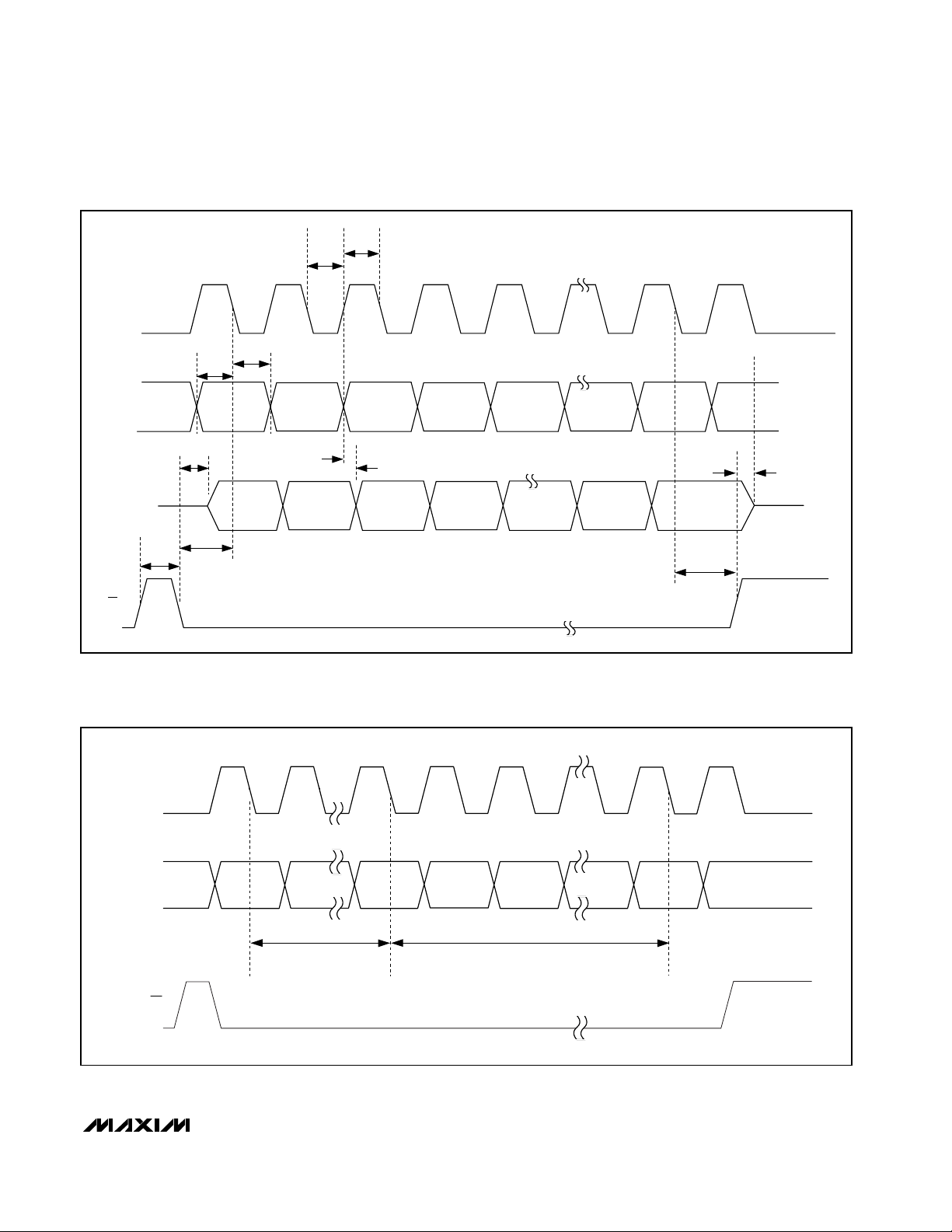
MAX1020–MAX1023/MAX1057/MAX1058
10-Bit, Multichannel ADCs/DACs with FIFO,
Temperature Sensing, and GPIO Ports
______________________________________________________________________________________ 39
Figure 11. DAC/GPIO Serial-Interface Timing (Clock Mode 11)
Figure 12. DAC-Select Register Byte and DAC Serial-Interface Word
SCLK
DIN
DOUT
t
CH
t
CL
1234
t
DH
t
DS
D15 D14 D13 D12 D11
t
DOE
D15
D7
t
t
CSPWH
CS
CSS
D14
D6
t
DOT
D13
D5
D12
D4
5
D1
32
16
8
D0
t
DOD
D1
D0
t
CSH
SCLK
DIN
DOUT
CS
1289
BIT 7 (MSB)
THE COMMAND BYTE
INITIALIZES THE DAC SELECT
REGISTER
BIT 6
BIT 0 (LSB)
BIT 15 BIT 14
10
THE NEXT 16 BITS SELECT THE DAC
AND THE DATA WRITTEN TO IT
24
BIT 0BIT 1
Page 40

MAX1020–MAX1023/MAX1057/MAX1058
10-Bit, Multichannel ADCs/DACs with FIFO,
Temperature Sensing, and GPIO Ports
40 ______________________________________________________________________________________
Figure 13. GPIO Timing
Figure 14.
LDAC
Functionality
LDAC
Functionality
Drive LDAC low to transfer the content of the input registers to the DAC registers. Drive LDAC permanently
low to make the DAC register transparent. The DAC
output typically settles from zero to full scale within ±1
LSB after 2µs. See Figure 14.
Layout, Grounding, and Bypassing
For best performance, use PC boards. Ensure that digital and analog signal lines are separated from each
other. Do not run analog and digital signals parallel to
one another (especially clock signals) or do not run
digital lines underneath the MAX1020–MAX1023/
MAX1057/MAX1058 package. High-frequency noise in
the AVDDpower supply may affect performance.
Bypass the AVDDsupply with a 0.1µF capacitor to
AGND, close to the AV
DD
pin. Bypass the DVDDsupply
with a 0.1µF capacitor to DGND, close to the DV
DD
pin.
Minimize capacitor lead lengths for best supply-noise
rejection. If the power supply is very noisy, connect a
10Ω resistor in series with the supply to improve powersupply filtering.
The MAX1020–MAX1023/MAX1057/MAX1058 thin QFN
packages contain an exposed pad on the underside of
the device. Connect this exposed pad to AGND. Refer to
the MAX1258EVKIT for an example of proper layout.
Definitions
Integral Nonlinearity
Integral nonlinearity (INL) is the deviation of the values
on an actual transfer function from a straight line. This
straight line can be either a best-straight-line fit or a line
drawn between the end points of the transfer function,
once offset and gain errors have been nullified. INL for
the MAX1020–MAX1023/MAX1057/MAX1058 is measured using the end-point method.
Differential Nonlinearity
Differential nonlinearity (DNL) is the difference between
an actual step width and the ideal value of 1 LSB. A
DNL error specification of less than 1 LSB guarantees
no missing codes and a monotonic transfer function.
CS
t
GOD
t
GPIO INPUT/OUTPUT
LDAC
GSU
t
LDACPWL
t
S
±1 LSB
OUT_
Page 41

MAX1020–MAX1023/MAX1057/MAX1058
10-Bit, Multichannel ADCs/DACs with FIFO,
Temperature Sensing, and GPIO Ports
______________________________________________________________________________________ 41
Unipolar ADC Offset Error
For an ideal converter, the first transition occurs at 0.5
LSB, above zero. Offset error is the amount of deviation
between the measured first transition point and the
ideal first transition point.
Bipolar ADC Offset Error
While in bipolar mode, the ADC’s ideal midscale transition occurs at AGND -0.5 LSB. Bipolar offset error is the
measured deviation from this ideal value.
ADC Gain Error
Gain error is defined as the amount of deviation
between the ideal transfer function and the measured
transfer function, with the offset error removed and with
a full-scale analog input voltage applied to the ADC,
resulting in all ones at DOUT.
DAC Offset Error
DAC offset error is determined by loading a code of all
zeros into the DAC and measuring the analog output
voltage.
DAC Gain Error
DAC gain error is defined as the amount of deviation
between the ideal transfer function and the measured
transfer function, with the offset error removed, when
loading a code of all ones into the DAC.
Aperture Jitter
Aperture jitter (tAJ) is the sample-to-sample variation in
the time between the samples.
Aperture Delay
Aperture delay (tAD) is the time between the rising
edge of the sampling clock and the instant when an
actual sample is taken.
Signal-to-Noise Ratio
For a waveform perfectly reconstructed from digital samples, signal-to-noise ratio (SNR) is the ratio of full-scale
analog input (RMS value) to the RMS quantization error
(residual error). The ideal, theoretical minimum analogto-digital noise is caused by quantization error only and
results directly from the ADC’s resolution (N bits):
SNR = (6.02 x N + 1.76)dB
In reality, there are other noise sources besides quantization noise, including thermal noise, reference noise,
clock jitter, etc. Therefore, SNR is calculated by taking
the ratio of the RMS signal to the RMS noise. RMS noise
includes all spectral components to the Nyquist frequency excluding the fundamental, the first five harmonics, and the DC offset.
Signal-to-Noise Plus Distortion
Signal-to-noise plus distortion (SINAD) is the ratio of the
fundamental input frequency’s RMS amplitude to the
RMS equivalent of all other ADC output signals:
SINAD(dB) = 20 x log (Signal
RMS
/ Noise
RMS
)
Effective Number of Bits
Effective number of bits (ENOB) indicates the global
accuracy of an ADC at a specific input frequency and
sampling rate. An ideal ADC’s error consists of quantization noise only. With an input range equal to the fullscale range of the ADC, calculate the ENOB as follows:
ENOB = (SINAD - 1.76) / 6.02
Total Harmonic Distortion
Total harmonic distortion (THD) is the ratio of the RMS
sum of the first five harmonics of the input signal to the
fundamental itself. This is expressed as:
where V1is the fundamental amplitude, and V2through
V6are the amplitudes of the first five harmonics.
Spurious-Free Dynamic Range
Spurious-free dynamic range (SFDR) is the ratio of RMS
amplitude of the fundamental (maximum signal component) to the RMS value of the next largest distortion
component.
ADC Channel-to-Channel Crosstalk
Bias the ON channel to midscale. Apply a full-scale sine
wave test tone to all OFF channels. Perform an FFT on
the ON channel. ADC channel-to-channel crosstalk is
expressed in dB as the amplitude of the FFT spur at the
frequency associated with the OFF channel test tone.
Intermodulation Distortion (IMD)
IMD is the total power of the intermodulation products
relative to the total input power when two tones, f1 and
f2, are present at the inputs. The intermodulation products are (f1 ± f2), (2 x f1), (2 x f2), (2 x f1 ± f2), (2 x f2 ±
f1). The individual input tone levels are at -7dB FS.
Small-Signal Bandwidth
A small -20dB FS analog input signal is applied to an
ADC so the signal’s slew rate does not limit the ADC’s
performance. The input frequency is then swept up to
the point where the amplitude of the digitized conversion result has decreased by -3dB. Note that the T/H
performance is usually the limiting factor for the smallsignal input bandwidth.
2
2
2
THD x VVVVVV= ++++
log /
20
()
2
3
4
2
5
621
Page 42

MAX1020–MAX1023/MAX1057/MAX1058
10-Bit, Multichannel ADCs/DACs with FIFO,
Temperature Sensing, and GPIO Ports
42 ______________________________________________________________________________________
Full-Power Bandwidth
A large -0.5dB FS analog input signal is applied to an
ADC, and the input frequency is swept up to the point
where the amplitude of the digitized conversion result
has decreased by -3dB. This point is defined as fullpower input bandwidth frequency.
DAC Digital Feedthrough
DAC digital feedthrough is the amount of noise that
appears on the DAC output when the DAC digital control lines are toggled.
ADC Power-Supply Rejection
ADC power-supply rejection (PSR) is defined as the
shift in offset error when the power-supply is moved
from the minimum operating voltage to the maximum
operating voltage.
DAC Power-Supply Rejection
DAC PSR is the amount of change in the converter’s
value at full-scale as the power-supply voltage changes
from its nominal value. PSR assumes the converter’s
linearity is unaffected by changes in the power-supply
voltage.
Chip Information
TRANSISTOR COUNT: 58,141
PROCESS: BiCMOS
Page 43

MAX1020–MAX1023/MAX1057/MAX1058
10-Bit, Multichannel ADCs/DACs with FIFO,
Temperature Sensing, and GPIO Ports
______________________________________________________________________________________ 43
Pin Configurations
TOP VIEW
GPIOA0
GPIOA1
EOC
DV
DD
DGND
DOUT
SCLK
DIN
OUT0
REF2/AIN6
AIN5
OUT2
N.C.
MAX1020
MAX1021
DD
AV
OUT3
CNVST/AIN7
363534333231302928
1
2
3
4
5
6
7
8
9
101112131415161718
OUT1
THIN QFN
N.C.
AGND
AIN4
N.C.
AIN3
OUT4
AIN2
OUT5
AIN1
27
AIN0
26
REF1
25
GPIOC1
24
GPIOC0
N.C.
23
RES_SEL
22
CS
21
LDAC
20
OUT7
19
OUT6
AIN13
AIN12
AIN10
AIN9
REF2/AIN14
4847464544434241403938
AIN11
AIN8
CNVST/AIN11
N.C.
EOC
DV
DGND
DOUT
SCLK
OUT0
AIN7
AIN6
AIN5
DIN
DD
AIN4
AIN9
AIN8
MAX1022
MAX1023
OUT3
OUT2
THIN QFN
AIN7
DD
AV
REF2/AIN10
363534333231302928
1
2
3
4
5
6
7
8
9
101112131415161718
OUT1
AIN3
37
N.C.
AGND
AIN6
N.C.
AIN5
OUT4
AIN4
OUT5
AIN3
OUT6
27
26
25
24
23
22
21
20
19
AIN2
REF1
AIN1
N.C.
AIN0
RES_SEL
CS
LDAC
OUT7
24OUT6
36
35
34
33
32
31
30
29
28
27
26
25
AIN2
REF1
AIN1
AIN0
GPIOC3
GPIOC2
GPIOC1
GPIOC0
RES_SEL
CS
LDAC
OUT7
CNVST/AIN15
EOC
1
2GPIOA0
3GPIOA1
4
5GPIOA2
6GPIOA3
7DV
DD
8DGND
9DOUT
10SCLK
11DIN
12OUT0
13
14OUT2
OUT1
MAX1057
MAX1058
15OUT31617GPIOB1
18AVDD19AGND
GPIOB0
20GPIOB2
21GPIOB3
22OUT4
23OUT5
THIN QFN
Page 44
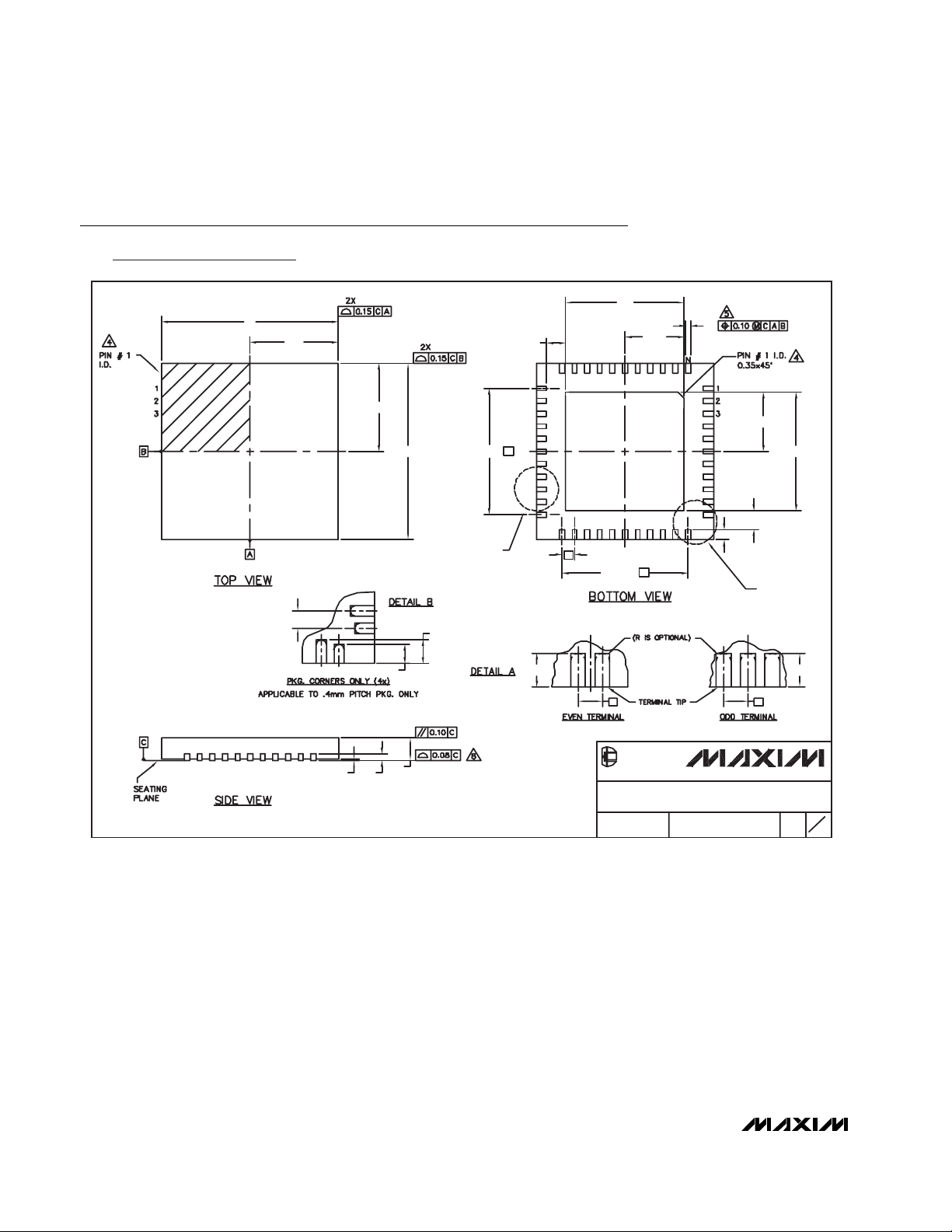
MAX1020–MAX1023/MAX1057/MAX1058
10-Bit, Multichannel ADCs/DACs with FIFO,
Temperature Sensing, and GPIO Ports
44 ______________________________________________________________________________________
Package Information
(The package drawing(s) in this data sheet may not reflect the most current specifications. For the latest package outline information,
go to www.maxim-ic.com/packages
.)
D/2
D2
C
L
k
D2/2
b
D
E/2
E
e
L1
A1AA2
(NE-1)Xe
DETAILA
L
e
(ND-1)Xe
C
L
L
e
DALLAS
SEMICONDUCTOR
PROPRIETARYINFORMATION
TITLE:
PACKAGEOUTLINE
32,44,48,56LTHINQFN,7x7x0.8mm
APPROVAL
DOCUMENTCONTROLNO.
21-0144
E2/2
C
E2
L
k
L
DETAILB
C
L
L
e
REV.
D
32, 44, 48L QFN.EPS
1
2
Page 45

MAX1020–MAX1023/MAX1057/MAX1058
10-Bit, Multichannel ADCs/DACs with FIFO,
Temperature Sensing, and GPIO Ports
______________________________________________________________________________________ 45
Package Information (continued)
(The package drawing(s) in this data sheet may not reflect the most current specifications. For the latest package outline information,
go to www.maxim-ic.com/packages
.)
DALLAS
SEMICONDUCTOR
PROPRIETARYINFORMATION
TITLE:
PACKAGEOUTLINE
32,44,48,56LTHINQFN,7x7x0.8mm
DOCUMENTCONTROLNO.APPROVAL
21-0144
REV.
2
2
D
Page 46

MAX1020–MAX1023/MAX1057/MAX1058
10-Bit, Multichannel ADCs/DACs with FIFO,
Temperature Sensing, and GPIO Ports
46 ______________________________________________________________________________________
Package Information (continued)
(The package drawing(s) in this data sheet may not reflect the most current specifications. For the latest package outline information,
go to www.maxim-ic.com/packages
.)
D
D/2
e
A1 A2
E/2
E
L1
A
(NE-1)Xe
L
k
D2
C
L
D2/2
(ND-1)Xe
C
L
e e
b
e
E2/2
C
E2
L
k
L
C
L
LL
QFN THIN 6x6x0.8.EPS
PACKAGEOUTLINE
36,40,48LTHINQFN, 6x6x0.8mm
21-0141
1
E
2
Page 47

MAX1020–MAX1023/MAX1057/MAX1058
10-Bit, Multichannel ADCs/DACs with FIFO,
Temperature Sensing, and GPIO Ports
Maxim cannot assume responsibility for use of any circuitry other than circuitry entirely embodied in a Maxim product. No circuit patent licenses are
implied. Maxim reserves the right to change the circuitry and specifications without notice at any time.
47 ____________________Maxim Integrated Products, 120 San Gabriel Drive, Sunnyvale, CA 94086 408-737-7600
© 2004 Maxim Integrated Products Printed USA is a registered trademark of Maxim Integrated Products.
Package Information (continued)
(The package drawing(s) in this data sheet may not reflect the most current specifications. For the latest package outline information,
go to www.maxim-ic.com/packages
.)
NOTES:
1.DIMENSIONING&TOLERANCINGCONFORM TOASMEY14.5M-1994.
2.ALLDIMENSIONSAREINMILLIMETERS.ANGLESAREINDEGREES.
3.NISTHETOTALNUMBER OFTERMINALS.
4.THETERMINAL#1IDENTIFIERANDTERMINALNUMBERINGCONVENTIONSHALLCONFORMTOJESD95-1
SPP-012.DETAILSOFTERMINAL#1IDENTIFIERAREOPTIONAL,BUTMUST BELOCATEDWITHINTHE
ZONEINDICATED.THETERMINAL#1IDENTIFIERMAYBEEITHERAMOLDORMARKEDFEATURE.
5.DIMENSIONbAPPLIESTOMETALLIZEDTERMINALANDISMEASUREDBETWEEN0.25mmAND0.30mm
FROMTERMINALTIP.
6.NDANDNEREFERTOTHENUMBEROFTERMINALSONEACHDANDESIDERESPECTIVELY.
7.DEPOPULATIONISPOSSIBLEINASYMMETRICALFASHION.
8.COPLANARITYAPPLIESTOTHEEXPOSEDHEATSINKSLUGASWELLASTHETERMINALS.
9.DRAWINGCONFORMSTOJEDECMO220,EXCEPT FOR0.4mmLEADPITCHPACKAGET4866-1.
10.WARPAGESHALLNOTEXCEED0.10mm.
PACKAGEOUTLINE
36,40,48LTHINQFN, 6x6x0.8mm
21-0141
2
E
2
Page 48

WWW.ALLDATASHEET.COM
Copyright © Each Manufacturing Company.
All Datasheets cannot be modified without permission.
This datasheet has been download from :
www.AllDataSheet.com
100% Free DataSheet Search Site.
Free Download.
No Register.
Fast Search System.
www.AllDataSheet.com
 Loading...