19-1109; Rev 0; 7/96
_______________General Description
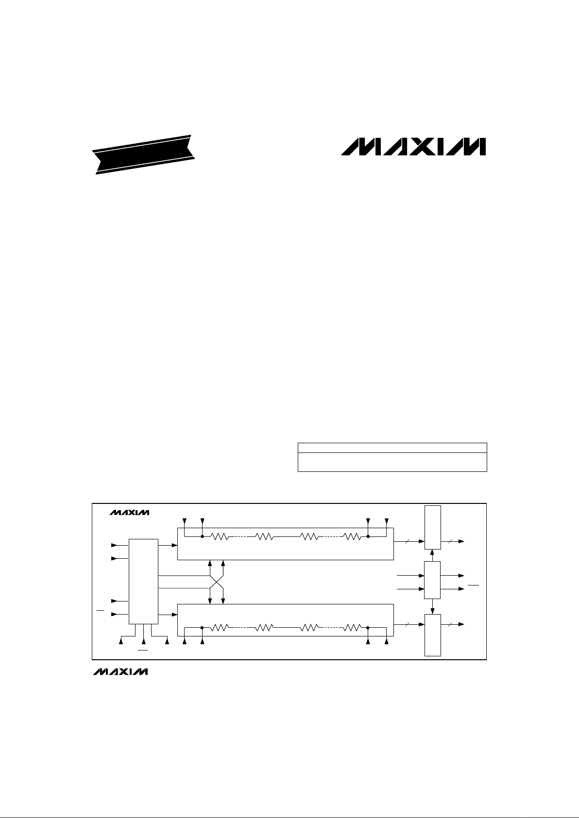
The MAX101A ECL-compatible, 500Msps, 8-bit analogto-digital converter (ADC) allows accurate digitizing of
analog signals from DC to 250MHz (Nyquist frequency). Dual monolithic converters, driven by the track/hold
(T/H), operate on opposite clock edges (time interleaved). Designed with Maxim’s proprietary advanced
bipolar processes, the MAX101A contains a high-performance T/H amplifier and two quantizers in an 84-pin
ceramic flat pack.
The innovative design of the internal T/H ensures an
exceptionally wide 1.2GHz input bandwidth and aperture delay uncertainty of less than 2ps, resulting in a
high 7.0 effective bits at the Nyquist frequency. Special
comparator output design and decoding circuitry
reduce out-of-sequence code errors. The probability of
erroneous codes due to metastable states is reduced to
less than 1 error per 1015clock cycles. And, unlike other
ADCs that can have errors resulting in false full-scale or
zero-scale outputs, the MAX101A keeps the error magnitude to less than 1LSB.
The analog input is designed for either differential or
single-ended use with a ±250mV range. Sense pins for
the reference input allow full-scale calibration of the
input range or facilitate ratiometric use.
Phase adjustment is available to adjust the relative
sampling of the converter halves for optimizing converter performance. Input clock phasing is also available
for interleaving several MAX101As for higher effective
sampling rates.
____________________________Features
♦ 500Msps Conversion Rate
♦ 7.0 Effective Bits Typical at 250MHz
♦ 1.2GHz Analog Input Bandwidth
♦ Less than ±1/2LSB INL
♦ 50Ω Differential or Single-Ended Inputs
♦ ±250mV Input Signal Range
♦ Ratiometric Reference Inputs
♦ Dual Latched Output Data Paths
♦ Low Error Rate, Less than 10
-15
Metastable States
♦ 84-Pin Ceramic Flat Pack
________________________Applications
High-Speed Digital Instrumentation
High-Speed Signal Processing
Medical Systems
Radar/Signal Processing
High-Energy Physics
Communications
______________Ordering Information
MAX101A
500Msps, 8-Bit ADC with Track/Hold
________________________________________________________________
Maxim Integrated Products
1
DCLK
DCLK
PH
ADJ
TRK1
TRK1
BDATA
ADATA
AIN+
AIN-
CLK
CLK
VA
RTVARTS VA
RB
VA
RBS
VB
RT
VB
RTS
VB
RB
VB
RBS
L
A
T
C
H
E
S
L
A
T
C
H
E
S
STROBESTROBE
TRACK
AND
HOLD
FLASH CONVERTER
(8 -BIT)
FLASH CONVERTER
(8 -BIT)
8 8
8 8
MAX101A
B
U
F
F
E
R
_________________________________________________________Functional Diagram
For the latest literature: http://www.maxim-ic.com, or phone 1-800-998-8800
PART
MAX101ACFR* 0°C to +70°C
TEMP. RANGE PIN-PACKAGE
84 Ceramic Flat Pack
(with heatsink)
EVALUATION KIT MANUAL
AVAILABLE
*Contact factory for 84-pin ceramic flat pack without heatsink.
MAX101A
500Msps, 8-Bit ADC with Track/Hold
2 _______________________________________________________________________________________
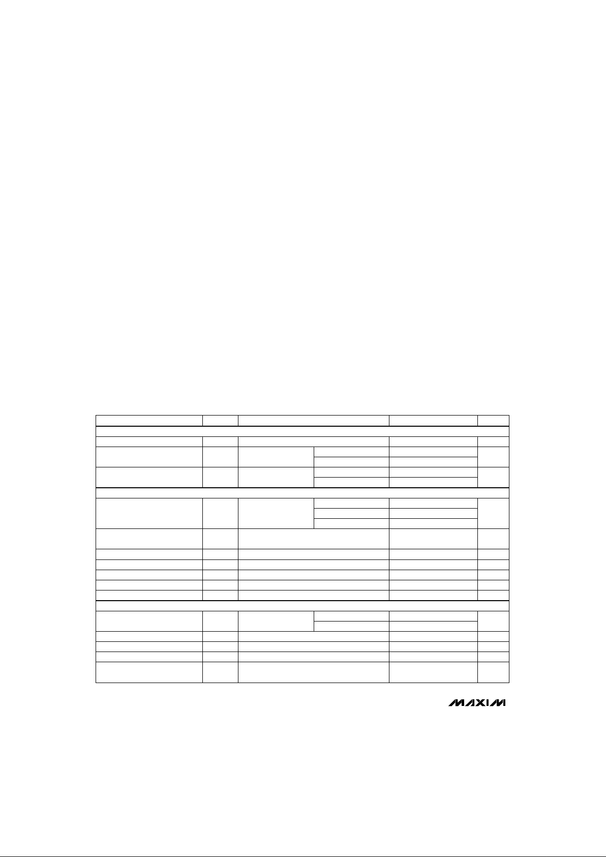
ABSOLUTE MAXIMUM RATINGS
ELECTRICAL CHARACTERISTICS
(VEE= -5.2V, VCC= +5V, RL= 100Ω to -2V, VART, VBRT= 0.95V, VARB, VBRB= -0.95V, TA= +25°C, unless otherwise noted.
T
MIN
to T
MAX
= 0°C to +70°C.) (Note 3)
Stresses beyond those listed under “Absolute Maximum Ratings” may cause permanent damage to the device. These are stress ratings only, and functional
operation of the device at these or any other conditions beyond those indicated in the operational sections of the specifications is not implied. Exposure to
absolute maximum rating conditions for extended periods may affect device reliability.
Supply Voltages (Note 1)
V
CC
...........................................................................0V to +7V
V
EE
.............................................................................-7V to 0V
V
CC
- VEE.........................................................................+12V
Analog Input Voltage.............................................................±2V
Reference Voltage (VA
RT
, VBRT)...........................-0.3V to +1.5V
Reference Voltage (VA
RB
, VBRB)..........................-1.5V to +0.3V
Clock Input Voltage (V
IH
, VIL).....................................-2.3V to 0V
DIV10 Input Voltage (VIH, VIL).......................................VEEto 0V
Output Current, (I
OUT(max)
)
T
J
<100°C.......................................................................14mA
100°C < T
J
<120°C.........................................................12mA
Operating Temperature Range...............................0°C to +70°C
Operating Junction Temperature (Note 2)............0°C to +120°C
Storage Temperature Range.............................-65°C to +150°C
Lead Temperature (soldering, 10sec).............................+250°C
Full scale
AData, BData,
no missing codes
f
CLK
= 500MHz,
VIN= 95% full scale
(Note 5)
Bits7.1
f
AIN
= 10MHz
f
AIN
= 125MHz
Zero scale
7.6
f
AIN
= 250MHz
AData, BData
6.7 7.0
ENOBEffective Bits
CONDITIONS
Figure 4
Figure 4
(Note 7)
f
AIN
= 125MHz, f
CLK
= 500MHz,
VIN= 95% full scale (Note 6)
ps2t
AJ
ps270t
AW
Aperture Width
Aperture Jitter
205 290
Msps500f
CLK
Maximum Conversion Rate
dB44.5SNRSignal-to-Noise Ratio
GHz1.2BW
3dB
Analog Input Bandwidth
AIN+ to AIN-, Table 2,
TA= T
MIN
to T
MAX
mV
-290 -205
V
IN
Input Voltage Range
AIN+, AIN-, to GND
TA= T
MIN
to T
MAX
±0.75
±0.50TA= +25°C
TA= T
MIN
to T
MAX
Bits8Resolution
AIN+, AIN-, TA= T
MIN
to T
MAX
Ω/°C0.008
Input Resistance
Temperature Coefficient
LSB
±0.75
INLIntegral Nonlinearity (Note 4)
Ω49 51R
I
Input Resistance
mV1.65 2.35LSB
mV-23 23V
IO
Input Offset Voltage
UNITSMIN TYP MAXSYMBOLPARAMETER
Least Significant Bit Size
TA= +25°C
TA= T
MIN
to T
MAX
LSB
±0.85
DNLDifferential Nonlinearity
Note 1: The digital control inputs are diode protected. However, limited protection is provided on other pins. Permanent damage
may occur on unconnected units under high-energy electrostatic fields. Keep unused units in supplied conductive carrier or
shunt the terminals together.
Note 2: Typical thermal resistance, junction-to-case R
θJC
= 5°C/W and thermal resistance, junction to ambient (MAX101ACFR)
R
θJA
=12°C/W, if 200 lineal ft/min airflow is provided. See
Package Information.
Figure 4 ns1t
AD
Aperture Delay
ACCURACY
DYNAMIC SPECIFICATIONS
ANALOG INPUT
VCC(nom) = ±0.25V
MAX101A
500Msps, 8-Bit ADC with Track/Hold
_______________________________________________________________________________________ 3
40
-1.02 -0.70
VARTto VA
RB
1.1 3.1
-50 50
TA= +25°C
-1.95 -1.60TA= +25°C
TA= T
MIN
to T
MAX
CONDITIONS
VEE= -5.2V
TA= +25°C
VCC= 5.0V
mA
-935
TA= +25°C
I
VEE
AData, BData
Negative Supply Current
TA= T
MIN
to T
MAX
-895 -500
V
INCM
= ±0.5V TA= T
MIN
to T
MAX
mA
910
I
VCC
Positive Supply Current
dBCMRRCommon-Mode Rejection Ratio 35
TA= T
MIN
to T
MAX
V
-1.95 -1.50
V
OL
Digital Output Low Voltage
dB
415 855
40VCC(nom) = ±0.25V
Power-Supply Rejection Ratio PSRR
V-1.50V
IL
Digital Input Low Voltage
Ω100 190R
REF
Reference String Resistance
Ω/°C0.02
Reference String Resistance
Temperature Coefficient
UNITSMIN TYP MAXSYMBOLPARAMETER
CLK, CLK, TA= T
MIN
to T
MAX
VV
IH
Digital Input High Voltage
CLK, CLK = -0.8V (no termination),
TA= T
MIN
to T
MAX
mA
-40 40
I
IH
TA= T
MIN
to T
MAX
AData, BData,
DCLK, DCLK
PH
ADJ
= 0V, TA= T
MIN
to T
MAX
V
-1.10 -0.60
V
OH
Digital Output High Voltage
Digital Input High Current
Input Bias Current I
B
µA
DIV10 = 0V, TA= T
MIN
to T
MAX
Clock Input Bias Current I
CLK
µA
-1.3 -1.00TA= +25°C
TA= T
MIN
to T
MAX
DCLK, DCLK
-1.4 -0.9
DCLK, DCLK, TA= T
MIN
to T
MAX
mV275 445V
OH
- V
OL
Digital Output Voltage
REFERENCE INPUT
LOGIC INPUTS
LOGIC OUTPUTS (Note 8)
POWER REQUIREMENTS
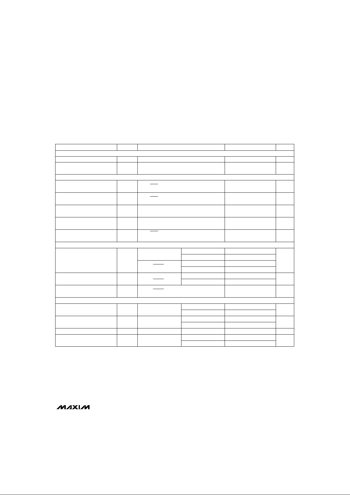
ELECTRICAL CHARACTERISTICS (continued)
(VEE= -5.2V, VCC= +5V, RL= 100Ω to -2V, VART, VBRT= 0.95V, VARB, VBRB= -0.95V, TA= +25°C, unless otherwise noted.
T
MIN
to T
MAX
= 0°C to +70°C.) (Note 3)
TA= T
MIN
to T
MAX
CLK, CLK, TA= T
MIN
to T
MAX
-1.1
VEE(nom) = ±0.25V
Divide-by-1 mode See
Figures 2, 3
MAX101A
500Msps, 8-Bit ADC with Track/Hold
4 _______________________________________________________________________________________
DIV10 = 0, Figures 1 and 2
DIV10 = 0, Figures 1 and 2
ns
CLK, CLK
CLK, CLK
0.7 1.3 1.8t
PD2
DCLK to A/BData
Propagation Delay
DCLK
DATA
DCLK
DATA
20% to 80% ps
800
t
F
ns1.2 2.3 3.4t
PD1
CLK to DCLK
Propagation Delay
CONDITIONS
20% to 80%
300
Clock
Cycles
t
NPD
Divide-by-1 mode, Figures 2 and 3, Table 1Pipeline Delay (Latency) 15 15
ps
500
t
R
Fall Time
300
Rise Time
ns0.9 2.5t
PWH
ns0.9 2.5t
PWL
Clock Pulse Width Low
Clock Pulse Width High
UNITSMIN TYP MAXSYMBOLPARAMETER
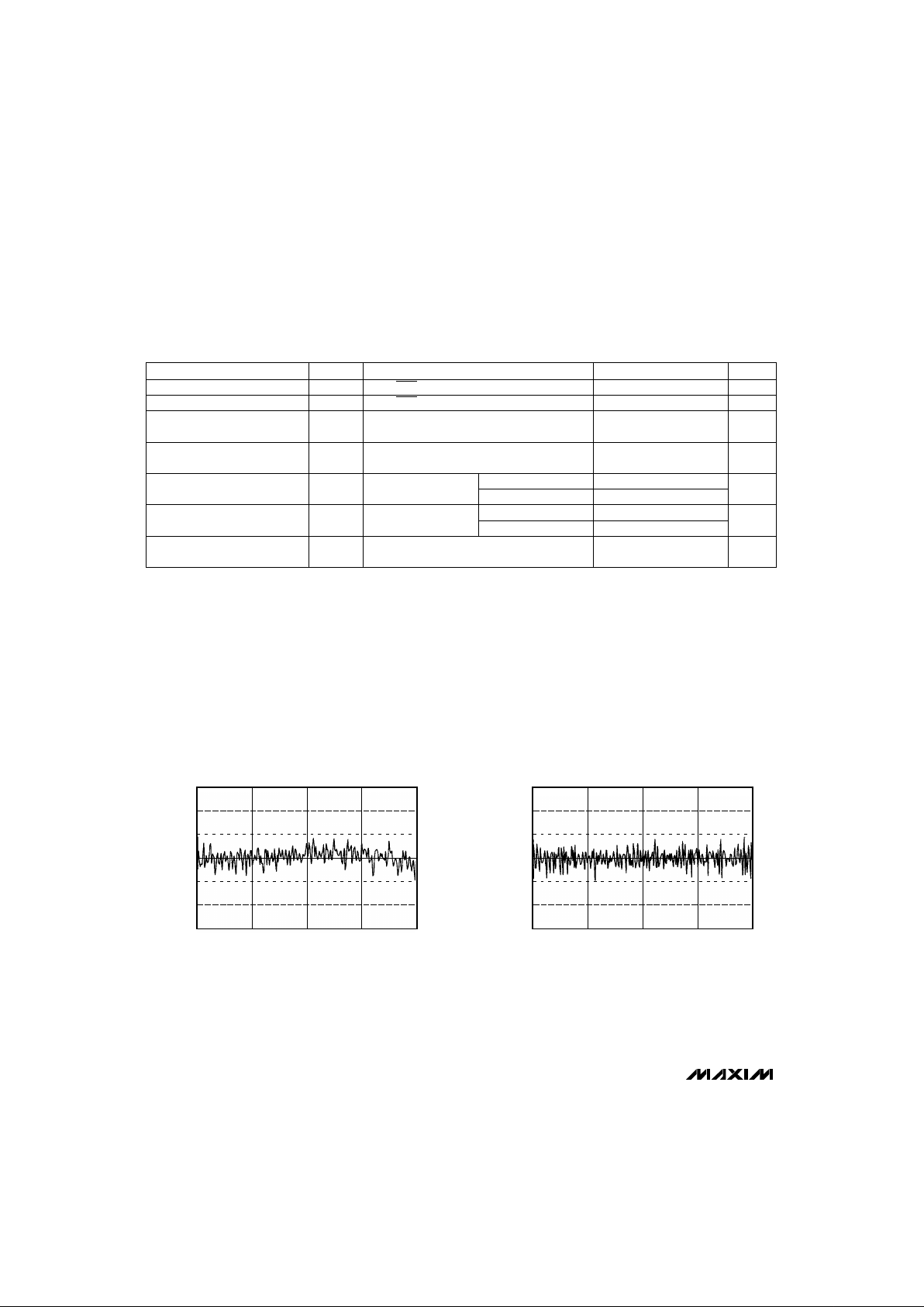
TIMING CHARACTERISTICS
(VEE= -5.2V, VCC= +5V, RL= 100Ω to -2V, VART, VBRT= 0.95V, VARB, VBRB= -0.95V, TA= +25°C, unless otherwise noted.)
Note 3: All devices are 100% production tested at +25°C and are guaranteed by design for T
A
= T
MIN
to T
MAX
as specified.
Note 4: Deviation from best-fit straight line. See
Integral Nonlinearity
section.
Note 5: See the
Signal-to-Noise Ratio and Effective Bits
section in the
Detailed Description of Specifications
.
Note 6: SNR calculated from effective bits performance using the following equation: SNR(dB) = 1.76 + 6.02 x effective bits.
Note 7: Clock pulse width minimum requirements t
PWL
and t
PWH
must be observed to achieve stated performance.
Note 8: Outputs terminated through 100Ω to -2.0V.
INTEGRAL NONLINEARITY
vs. OUTPUT CODE
-0.75
0.75
0 256
-0.50
0.50
MAX101 TOC1
OUTPUT CODE
INL (LSBs)
64 192128
0
-0.25
0.25
DIFFERENTIAL NONLINEARITY
vs. OUTPUT CODE
-0.75
0.75
0 256
-0.50
0.50
MAX101 TOC2
OUTPUT CODE
DNL (LSBs)
64 192128
0
-0.25
0.25
__________________________________________Typical Operating Characteristics
(VEE= -5.2V, VCC= +5V, RL= 100Ω to -2V, VART, VBRT= 0.95V, VARB, VBRB= -0.95V, TA= +25°C, unless otherwise noted.)
MAX101A
500Msps, 8-Bit ADC with Track/Hold
_______________________________________________________________________________________
5
____________________________Typical Operating Characteristics (continued)
(VEE= -5.2V, VCC= +5V, RL= 100Ω to -2V, VART, VBRT= 0.95V, VARB, VBRB= -0.95V, TA= +25°C, unless otherwise noted.)
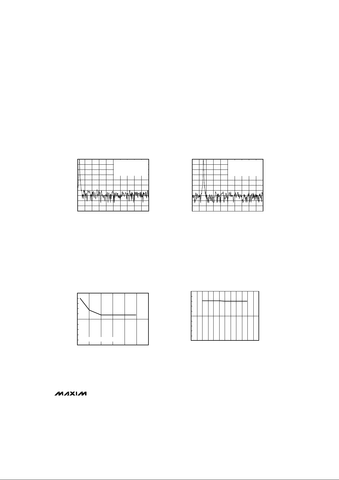
FFT PLOT
(f
AIN
= 251.4462MHz)
-100
-40
-30
-20
-10
0
0 50 75 100 125
-90
-50
MAX101 TOC3
(MHz)
(dB)
25
-70
-80
-60
f
CLK
= 500MHz
SER = -44.5dB
NOISE FLOOR = -67.3dB
SPURIOUS = -58.2dB
FFT PLOT
(f
AIN
= 10.4462MHz)
-100
-40
-30
-20
-10
0
0 25 37.5 50 62.5
-90
-50
MAX101 TOC4
(MHz)
(dB)
12.5
-70
-80
-60
f
CLK
= 250MHz
SER = -47.2dB
NOISE FLOOR = -70.5dB
SPURIOUS = -61.8dB
EFFECTIVE BITS vs. ANALOG INPUT
FREQUENCY (f
AIN
)
(f
CLK
= 500MHz, VIN = 95% FS)
MAX110 TOC5
6
500
7
8
f
AIN
(MHz)
100 150 200 250 300
EFFECTIVE BITS
RECORD LENGTH = 512
EFFECTIVE BITS vs. CLOCK
FREQUENCY (f
CLK
)
(f
AIN
= 10.4462, VIN = 95% FS)
MAX110 TOC6
6
1000
7
8
f
CLK
(MHz)
200 300 400 500 600
EFFECTIVE BITS
 Loading...