MAXIM MAX1011 Technical data

Quick Start
The MAX1011 EV kit is fully assembled and tested.
Follow these steps to verify proper board operation. Do
not turn on the power supplies until all connections
to the EV kit are completed.
1) Connect a +5V power supply to the pad marked
VCC. Connect this supply’s ground to the pad
marked GND.
2) Connect a +3.3V power supply to the pad labeled
VCCO. Connect the supply ground to the pad
marked OGND.
3) Connect a +3.7V power supply to the pad marked
VTUNE. Connect the supply ground to the GND
pad.
4) Remove the shunt from jumper JU5. This sets a
250mVp-p full-scale range.
General Description
The MAX1011 evaluation kit (EV kit) simplifies evaluation
of the 90Msps MAX1011 6-bit analog-to-digital converter
(ADC). The kit includes the basic components necessary
to operate the on-chip oscillator as a voltage-controlled
oscillator (VCO). The board can also be easily modified to
accommodate an external clocking source.
Connectors for power supplies, analog inputs, and digital
outputs simplify connections to the device. The PC board
features an optimized layout to ensure the best possible
dynamic performance. The EV kit includes a MAX1011.
Features
♦ 5.85 Effective Number of Bits at 20MHz Analog
Input Frequency
♦ Separate Analog and Digital Power and Ground
Connections with Optimized PC Board Layout
♦ Single-Ended or Differential Analog Input
♦ Square-Pin Header for Easy Connection of Logic
Analyzer to Digital Outputs
♦ User-Selectable ADC Full-Scale Gain Ranges
♦ Fully Assembled and Tested Surface-Mount
Board
Evaluates: MAX1011
MAX1011 Evaluation Kit
________________________________________________________________
Maxim Integrated Products
1
SUPPLIER* PHONE FAX
AVX (803) 946-0690 (803) 626-3123
Component Suppliers
Component List
Ordering Information
For free samples & the latest literature: http://www.maxim-ic.com, or phone 1-800-998-8800
For small orders, phone 408-737-7600 ext. 3468.
Coilcraft (847) 639-6400 (847) 639-1469
M/A-COM (617) 564-3100 (617) 564-3050
Sprague (603) 224-1961 (603) 224-1430
*
Please indicate that you are using the MAX1011 when contacting these component suppliers.
PART
MAX1011EVKIT 0°C to +70°C
TEMP. RANGE IC PACKAGE
24 QSOP
DESIGNATION QTY DESCRIPTION
C1, C3,
C5
3
0.01µF, 10V min, 10% ceramic
capacitors
C2, C7,
C8
3 47pF, 10V min, 5% ceramic capacitors
C4 1
0.22µF, 10V min, 10% ceramic
capacitor
C6 1 5pF, 10V min, 10% ceramic capacitor
C9, C10 2
0.1µF, 10V min, 10% ceramic
capacitors
D1 1
Varactor diode
M/A-COM MA4ST079CK-287, SOT23
JU1, JU2, JU6 3 0Ω resistors
JU3, JU4 2 2-pin headers
JU5 1 3-pin header
C11, C12 2
10µF, 10V min, 20% tantalum caps
AVX TAJC106K016
J1 1 14-pin connector
R2, R3 2 47kΩ, 5% resistors
R4, R5 2 49.9Ω, 1% resistors
None 1
MAX1011CEG
IN+, IN- 2 BNC connectors
Clock
Overdrive
0 Not Supplied
MAX1011 circuit board
None 1 Shunt for JU5
U1 1
R1 1 10kΩ, 5% resistor
L1 1
220nH inductor
Coilcraft 1008CS-221XKB
19-1335; Rev 0a; 2/98
查询MAX1011EVKIT供应商

Evaluates: MAX1011
5) Connect a 250mVp-p, 20MHz sine-wave source to
the analog input at BNC J3. The analog input is terminated in 50Ω (R4).
6) Connect a logic analyzer to connector J1 to monitor
the digital outputs.
7) Turn on all power supplies and signal sources.
8) Observe the digitized analog input signals with the
logic analyzer.
_______________Detailed Description
EV Kit Jumpers
The MAX1011 EV kit contains several jumpers that control board and part options. The following sections
describe the different jumpers and their purposes.
Table 1 lists the jumpers on the EV kit and their default
positions.
Analog Supply Power Requirements
The MAX1011 requires a +5V at approximately 37mA for
the analog VCCsupply. 0Ω resistors are installed at
jumper sites JU1, JU2, and JU6 and can be removed to
sense device power-supply currents with an ammeter.
Digital Outputs Supply
The MAX1011 requires +3.3V for the V
CCO
supply. The
current requirement from the power supply is a function
of the sampling clock and analog input frequencies, as
well as the capacitive loading on the digital outputs.
With 15pF loads and a 20MHz analog input frequency
sampled at 90Msps, the current draw is approximately
8.5mA.
Analog Inputs
The analog inputs to the ADC are provided through
BNC connectors IN+, and IN-. The connectors are terminated with 49.9Ω to ground and are AC coupled to
the converter’s analog inputs, which are internally selfbiased at 2.35V DC. A typical application circuit drives
the IN+ noninverting analog input using AC-coupled
signals. The nominal 20kΩ input resistance of the ana-
log inputs, plus the 0.1µF AC-coupling capacitor value,
sets the low-frequency corner at approximately 80Hz.
You can drive the analog inputs either single-ended or
differentially using AC- or DC-coupled inputs. Either the
inverting or the noninverting input can be driven singleended. If the inverting input is driven, then the digital
output codes are inverted (complemented). Refer to the
MAX1011 data sheet for typical circuits.
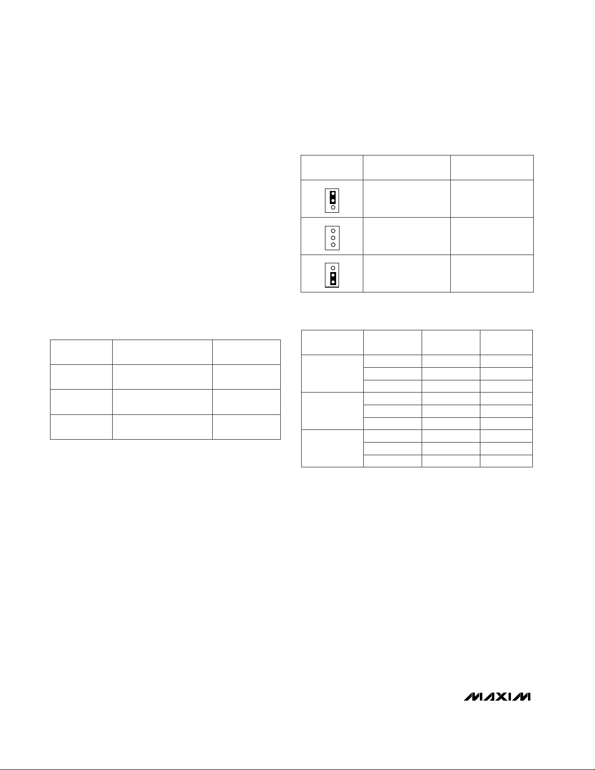
ADC Gain Selection
The single GAIN-select pin on the MAX1011 controls
the full-scale input range. Jumper JU5 is used to manually select the desired gain range as shown in Table 2.
The EV kits are shipped with the mid-gain range selected (jumper pins open).
Table 3 lists the possible input-drive combinations
for the mid-gain (250mVp-p) full-scale range selection.
Drive levels are referenced to the open-circuit,
common-mode voltage of the analog inputs (typically
MAX1011 Evaluation Kit
2 _______________________________________________________________________________________
Open
Offset-correction
amplifier enabled
JU3, JU4
Shorted with 0Ω
resistors
Power-supply currentsense ports
JU1, JU2,
JU6
DEFAULT
POSITION
FUNCTIONJUMPER(S)
Open
ADC full-scale range
selection
JU5
Mid-gain, 250mVp-p
OPEN
Low-gain, 500mVp-pGND
ADC GAIN RANGE
MAX1011 GAIN
CONTROL PIN
JU5 SETTING
High-gain, 125mVp-pV
CC
INPUT DRIVE
Single-Ended
Noninverting
0
+125mV
IN+
-125mV
Open Circuit
Open Circuit
IN-
Open Circuit
100000
111111
OUTPUT
CODE
000000
Open Circuit
Open Circuit
Open Circuit
0
+125mV
-125mV
Single-Ended
Inverting
011111
000000
111111
0
+62.5mV
-62.5mV
0
-62.5mV
+62.5mV
Differential
100000
111111
000000
JU5
1
2
3
JU5
1
2
3
JU5
1
2
3
Table 1. EV Kit Jumpers and Default
Positions
Table 2. Gain-Selection Jumper JU5
Settings
Table 3. Typical Input-Drive Requirements
for Mid-Gain

Evaluates: MAX1011
MAX1011 Evaluation Kit
_______________________________________________________________________________________ 3
2.35V) if DC coupled, or to ground if AC coupling is
used. If the low-gain (500mVp-p) range is selected, the
input-drive requirements are twice those listed in Table
3. If the high-gain (125mVp-p) range is selected, the
input-drive requirements are half those listed in Table 3.
Offset-Correction Amplifier
The offset-correction amplifier included on the
MAX1011 is usually enabled in a typical AC-coupled
application circuit. For DC-coupled applications, the
amplifier must be disabled by installing shorting blocks
on jumpers JU3 and JU4. These jumpers short device
pins OCC+ (pin 2) and OCC- (pin 3) to ground and disable the amplifier. The MAX1011 EV kit is configured
with the offset-correction amplifier enabled (jumpers
open) and AC-coupled analog inputs.
Voltage-Controlled-Oscillator Operation
The EV kit includes a voltage-controlled-oscillator
(VCO) circuit to set the analog-to-digital converter
(ADC) sampling rate using an external resonant tank
and a varactor diode. A voltage applied to the VTUNE
pad changes the varactor diode’s capacitance to
adjust the tank’s resonant frequency, which sets the
oscillator’s sampling frequency. VTUNE voltage can be
varied from 0V to a maximum of 8V.
The EV kit is designed so that a nominal VTUNE control
voltage of about 3.7V sets the ADC sampling rate to
90Msps. The VTUNE control voltage should be well filtered, as any noise on the supply contributes to jitter in
the internal oscillator and degrades the converter’s
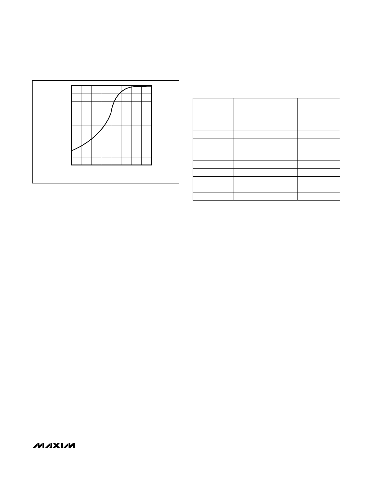
dynamic performance. Figure 1 shows the VTUNE
control-voltage typical frequency-adjustment range for
the MAX1011 EV kit (for VCO mode, refer to schematic
in Figure 2).
External Clock Operation
The MAX1011 EV kit can be converted to drive the ADC
from an external clock source. This involves removing
the external resonator components from the VCO circuit
and adding a few new components. Table 4 lists the EV
kit changes required to convert the board to accept an
external clock source. The resulting schematic is
shown in Figure 3.
The new 49.9Ω value of R3 shown in Figure 3 provides
proper termination for a 50Ω external signal generator.
AC-coupling capacitor C7 couples the external clock
signal to the MAX1011 oscillator circuitry at TNK+ (pin
7). R2 and C8 ensure that the impedance at both ports
of the oscillator is balanced. After all modifications are
complete, connect an external clock source to the BNC
connector on the EV kit marked CLOCK OVERDRIVE
(J2). The recommended clock amplitude is 1Vp-p; however, the ADC operates correctly with as little as
300mVp-p or up to 1.25Vp-p on CLOCK OVERDRIVE.
The external clock source should have low-phase noise
for best dynamic performance. A low-phase-noise
sine-wave oscillator serves this purpose well. A squarewave clock source is not necessary to drive the
MAX1011. The device contains sufficient gain to amplify even a low-level-input sine wave to drive the ADC
comparators, while ensuring excellent dynamic performance.
60
70
65
80
75
90
85
95
105
100
110
0 2 31 4 5 6 7 8
MAX1011 Fig01
VTUNE CONTROL VOLTAGE (V)
FREQUENCY (MHz)
Figure 1. MAX1011 Oscillator Frequency vs. VTUNE Control
Voltage
D1 RemoveVaractor diode
R1
R2, R3
L1
Replace with
49.9Ω resistors
47kΩ resistors
Remove
Remove
220nH inductor
10kΩ resistor
Replace with
0.01µF capacitors
MODIFICATION
Add
Remove
C6
C7, C8
Clock Overdrive
(J2)
COMPONENT
47pF capacitors
DESCRIPTION
Clock input BNC
connector
5pF capacitor
Table 4. External Clock Source EV Kit
Modifications
 Loading...