

________________General Description
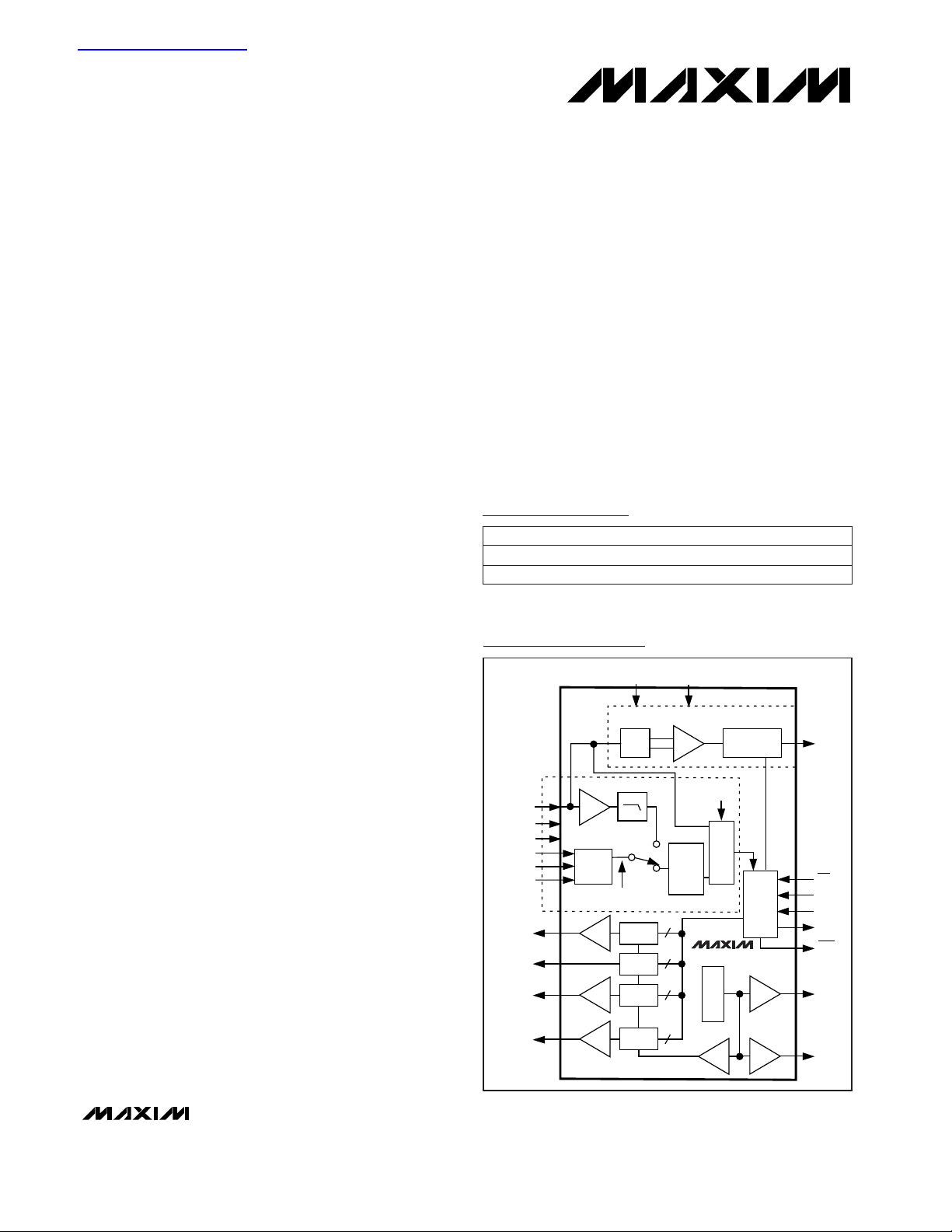
The MAX1007 is a multifunctional integrated circuit
designed for high-performance mobile radios. It
includes one 8-bit analog-to-digital converter (ADC),
and two 7-bit and two 6-bit digital-to-analog converters
(DACs) for functions including radio-frequency (RF)
power sensing and antenna-diversity selection.
The ADC provides for power sense, receive-signal
strength intensity (RSSI) measurements and system
supervision. In the power-sense mode, the ADC converts the power-sensing circuitry signal (representing
either the transmitted (Tx) or received (Rx) RF power)
into a digital code, ensuring optimum Tx power setting
and Rx signal analysis. An additional direct input to the
ADC provides for system-supervision measurements,
such as power-supply voltages, battery voltage, and
temperature.
Four DAC blocks typically control DC levels in radios.
As part of the Maxim PWT1900 chip set, the two 7-bit
DACs control the gain settings and the two 6-bit DACs
control the varactor diodes to tune a TCXO and bias a
GaAs amplifier. Each DAC register and output can be
updated independently, providing maximum flexibility.
For antenna diversity, a magnitude-comparison circuit
captures and compares two peak signals. A latched
logic-comparator output reveals which signal has the
largest magnitude. The MAX1007 also includes an onboard voltage reference for the ADC and DACs.
The MAX1007 offers a high level of signal integrity with
minimal power dissipation. Single-supply operation
ranges from +2.85V to +3.6V. To further save power, there
are two shutdown modes: standby and total shutdown.
Standby is a partial shutdown that keeps the bandgap
reference and the 2.4V reference generator active. Total
shutdown disables all circuit blocks except the serial
interface, reducing supply current to less than 1µA.
The MAX1007 is available in a 24-pin SSOP and is
specified for commercial and extended temperature
ranges.
________________________Applications
PWT1900
Wireless Communications:
Cellular Radios PMR/SMR
PCS Radios WLL
____________________________Features
♦ Multi-Input 8-Bit ADC
♦ Two 7-Bit DACs with Buffered Outputs
♦ Two 6-Bit DACs: Buffered/Unbuffered
♦ Power-Sense Conditioning Circuitry
♦ RSSI Measurement
♦ Antenna-Diversity Circuitry
♦ Internal Reference
♦ Serial-Logic Interface
♦ +2.85V to +3.6V Single-Supply Operation
♦ Two Shutdown Modes
MAX1007
Mobile-Radio Analog Controller
________________________________________________________________
Maxim Integrated Products
1
19-1180; Rev 0; 6/98
PART
MAX1007CAG
MAX1007EAG -40°C to +85°C
0°C to +70°C
TEMP. RANGE PIN-PACKAGE
24 SSOP
24 SSOP
Ordering Information
Pin Configuration appears at end of data sheet.
CS
SCLK
DIN
7
DOUT
SDAC
CH0
ADC
PEAK
DETECTOR
POWER
SENSE
RPS
RSSI
FPS1
FPS2
SDAC
XDAC
SDG
GDAC
KDAC
CH1
REFERENCE
PSBIAS
SERIAL
INTERFACE
PSDCTRL
PREAMBLE-SWITCHED DIVERSITY
POWER SENSE CIRCUITRY
PSDWDW
DUAL
T/H
VREF
XDAC
GDAC
KDAC
REF
PSOUT
BANT
ADC CTRL
PKWDW
6
6
7
D FLIP-FLOP
MAX1007
Functional Diagram
For free samples & the latest literature: http://www.maxim-ic.com, or phone 1-800-998-8800.
For small orders, phone 408-737-7600 ext. 3468.
查询MAX1007供应商

MAX1007
Mobile-Radio Analog Controller
2 _______________________________________________________________________________________
ABSOLUTE MAXIMUM RATINGS
ELECTRICAL CHARACTERISTICS
(AVDD= DVDD= +2.85V to +3.6V, f
SCLK
= 1.152MHz, TA= T
MIN
to T
MAX
, unless otherwise noted.)
Stresses beyond those listed under “Absolute Maximum Ratings” may cause permanent damage to the device. These are stress ratings only, and functional
operation of the device at these or any other conditions beyond those indicated in the operational sections of the specifications is not implied. Exposure to
absolute maximum rating conditions for extended periods may affect device reliability.
AVDDor DVDDto AGND or DGND...........................-0.3V to +6V
Digital Inputs to DGND.............................................-0.3V to +6V
Analog Inputs to AGND............................................-0.3V to +6V
REF to AGND............................................................-0.3V to +6V
AGND to DGND.................................................................± 0.3V
AV
DD
to DVDD....................................................................± 0.3V
Maximum Current into Any Pin............................................50mA
Continuous Power Dissipation (T
A
= +70°C)
SSOP (derate 8.0mW/°C above +70°C) ......................640mW
Operating Temperature Ranges
MAX1007CAG.....................................................0°C to +70°C
MAX1007EAG..................................................-40°C to +85°C
Storage Temperature Range.............................-65°C to +150°C
Lead Temperature (soldering, 10sec).............................+300°C
AVDD, DV
DD
RxEN = 1, TxEN = 1; AVDD= DVDD= 3V
RxEN = 1, TxEN = 0; AVDD= DVDD= 3V; PKWDW and
ADCCTRL as per state B on Figure 1
RxEN = 1, TxEN = 0; AVDD= DVDD= 3V;
PKWDW = ADCCTRL = DGND
RxEN = 1, TxEN = 0; AVDD= DVDD= 3V; PKWDW and
ADCCTRL as per state B on Figure 1. PSDWDW and PSDCNTRL as per state D on Figure 2
RxEN = 0, TxEN = 1; AVDD= DVDD= 3V;
PKWDW = ADCCTRL = DGND
RxEN = 0, TxEN = 1; AVDD= DVDD= 3V;
PKWDW and ADCCTRL as per state B on Figure 1
RxEN = 1, TxEN = 0; AVDD= DVDD= 3V; PKWDW and
ADCCTRL as per state C on Figure 1
RxEN = 0, TxEN = 1; AVDD= DVDD= 3V;
PKWDW and ADCCTRL as per state C on Figure 1
CONDITIONS
mA1.24 3.5
Standby:
XDAC, GDAC, Ref, RefBuf Active
mA4.07 10.5
Receive Mode 4:
KDAC, XDAC, ADC, RSSI
Buffer, Ref, RefBuf, PSD
Circuit Active
mA11.2 31
Receive Mode 3:
KDAC, XDAC, ADC, Peak
Detector RSSI Buffer, Ref,
RefBuf Active
V2.85 3.0 3.6Supply Voltages
mA2.95
Receive Mode 2:
KDAC, XDAC, Peak Detector,
RSSI Buffer, Ref, RefBuf Active
mA1.24 3.5
Receive Mode 1:
KDAC, XDAC, Ref, RefBuf
Active
mA1.8 5.0
Transmit Mode 1:
All DACs, Ref, RefBuf Active
mA4.7
Transmit Mode 2:
All DACs, PGA, REF, Peak
Detector, PSBIAS, I
SOURCE
,
RefBuf Active
mA12.2 32
Transmit Mode 3:
All DACs, PGA, REF, Peak
Detector, PSBIAS, I
SOURCE
,
RefBuf, ADC Active
UNITSMIN TYP MAXPARAMETER
RxEN = 0, TxEN = 0; AVDD= DVDD= 3V;
ADCCTRL = PSDCTRL = PKWDW = PSDWDW = DGND;
SCLK not active, either high or low
µA1 10Total Shutdown
POWER-SUPPLY REQUIREMENTS
SUPPLY CURRENTS [I(AVDD) + I(DVDD)] (Note 1)

MAX1007
Mobile-Radio Analog Controller
_______________________________________________________________________________________ 3
ELECTRICAL CHARACTERISTICS (continued)
(AVDD= DVDD= +2.85V to +3.6V, f
SCLK
= 1.152MHz, TA= T
MIN
to T
MAX
, unless otherwise noted.)
(Note 2)
2 < code ≤ FS
2 < code ≤ FS
2 < code ≤ FS
CL= 30pF, RL= 40kΩ, settling to 5% of final value
RL= 40kΩ
2 < code ≤ FS
(Note 2)
2 < code ≤ FS
(Note 2)
CL= 30pF, RL= 40kΩ
No resistive load
2 < code ≤ FS
CONDITIONS
%FSR±10Gain Error
LSB±1Offset Error
LSB±1Integral Nonlinearity
LSB±1Differential Nonlinearity
Bits7Resolution
µs4Full-Scale Step Response Time
V2.1 2.42 2.75Full-Scale Output Swing
V/µs0.1Output Slew Rate
%FSR±10Gain Error
LSB±1Offset Error
LSB±1Integral Nonlinearity
LSB±1Differential Nonlinearity
Bits6Resolution
LSB±1Differential Nonlinearity
Bits6Resolution
kΩ30Output Resistance
LSB±1/2Integral Nonlinearity
LSB±1Offset Error
%FSR±10Gain Error
V2.1 2.42 2.75Full-Scale Output Swing
UNITSMIN TYP MAXPARAMETER
CL= 30pF, RL= 40kΩ, settling to 2% of final value
RL= 40kΩ
CL= 30pF, RL= 40kΩ
µs4Full-Scale Step Response Time
V2.1 2.42 2.75Full-Scale Output Swing
V/µs0.1Output Slew Rate
CL= 30pF, RL= 40kΩ, settling to within 2% of final value µs4Power-Up Time from Standby
With respect to V
REF
V
REF
= 1.028V (typ)
V
REF
= 1.028V (typ)
LSB±5Gain Error
LSB±2Offset Error
µs5.2Conversion Time
LSB±1Integral Nonlinearity
LSB±1Differential Nonlinearity
V0 V
REF
Input Signal Range
Bits8Resolution
µs1.74
ADC Power-Up Time from Standby
V1.028Reference Voltage
XDAC
GDAC
SDAC, KDAC
ADC
MAX1007
Mobile-Radio Analog Controller
4 _______________________________________________________________________________________
ELECTRICAL CHARACTERISTICS (continued)
(AVDD= DVDD= +2.85V to +3.6V, f
SCLK
= 1.152MHz, TA= T
MIN
to T
MAX
, unless otherwise noted.)
V
IL
V
IH
SYMBOL
V0.3V
DD
Input Voltage Low
V0.7V
DD
Input Voltage High
V2.42Internal DAC Reference
µA200PS Bias Sink Current
V1.87PS Bias Voltage Output
V0.96 1.028 1.1Output Voltage
mV100 300Minimum Peak Level Detected
µs10 20Lowpass-Filter Time Constant
Ω200Pull-Down Input Resistance
µA50 100 180Current Source
-0.44
-6
VV
REF
Maximum Peak Level Detected
mV150Offset Voltage
V/V
-0.53
Power-Sense Amp Gain (PGA)
UNITSMIN TYP MAXPARAMETER
C
IN
R
IN
I
IN
pF10Inpt Capacitance
kΩ20Input Resistance
µA±1Input Current
t
8
t
7
t
6
t
5
t
4
t
3
t
2
t
1
ns100
CS High to DOUT Disable
ns200 434SCLK Pulse Width Low
ns200 434SCLK Pulse Width High
ns150SCLK High to DOUT Valid
ns100
CS Low to DOUT Valid
ns20
CS Low to SCLKHigh
ns0DIN to SCLK Hold
ns100DIN Valid to SCLK Setup
t
9
ns500
ADC Data Output Delay After
End of ADC Conversion
(Figure 4b)
V
OL
V
OH
V0.4Output Voltage Low
VVDD- 0.4Output Voltage High
CL= 20pF, RL= 100kΩ
RSin series with CL, CL= 1nF, 200Ω ≤ RS≤ 1kΩ
RPS, FPS1, FPS2 pulled to AGND when not
selected
Figure 3b
RSin series with CL, CL= 1nF, 200Ω ≤ RS≤ 1kΩ
Reflected transmit, classes 2, 3, 4
Reflected transmit, class 1
RPS, FPS1, FPS2 to ADC input
Forward transmit
CONDITIONS
CL= 20pF, RL= 100kΩ
Digital inputs
PSDCTRL, PSDWDW
Excluding PSDCTRL, PSDWDW
CL= 20pF
Digital Outputs (DOUT, BANT, SDG)
TIMING SPECIFICATIONS (Figure 4)
Digital Inputs (CS, SCLK, DIN, PKWDW, ADCCTRL, PSDWDW, PSDCTRL)
SERIAL-LOGIC INTERFACE
REFERENCE
TRANSMIT POWER SENSE
RSSI CIRCUIT

-0.5
-0.2
-0.3
-0.4
-0.1
0
0.1
0.2
0.3
0.4
0.5
0 10050 150 200 250 300
DIFFERENTIAL NONLINEARITY
MAX1007-01
CODES
DNL (LSBs)
1.25
1.35
1.30
1.45
1.40
1.50
1.55
-40 25 85
SUPPLY CURRENT vs. TEMPERATURE
(Tx MODE)
MAX1007-02
TEMPERATURE (°C)
SUPPLY CURRENT (mA)
VDD = 3.6V
VDD = 2.85V
1.80
2.00
1.90
2.20
2.10
2.30
2.40
25-40 85
SUPPLY CURRENT vs. TEMPERATURE
(Rx MODE)
MAX1007-03
TEMPERATURE (°C)
SUPPLY CURRENT (mA)
VDD = 3.6V
VDD = 2.85V
1.019
1.022
1.021
1.020
1.023
1.024
1.025
-5-40 25 55 85
REFERENCE VOLTAGE
vs. TEMPERATURE
MAX1007-04
TEMPERATURE (°C)
REFERENCE VOLTAGE (V)
VDD = 3.6V
VDD = 2.85V
1.76
1.82
1.80
1.78
1.84
1.86
-5-40 25 55 85
PS BIAS VOLTAGE vs. TEMPERATURE
MAX1007-05
TEMPERATURE (°C)
PS BIAS VOLTAGE (V)
VDD = 3.6V
VDD = 2.85V
MAX1007
Mobile-Radio Analog Controller
_______________________________________________________________________________________ 5
ELECTRICAL CHARACTERISTICS (continued)
(AVDD= DVDD= +2.85V to +3.6V, f
SCLK
= 1.152MHz, TA= T
MIN
to T
MAX
, unless otherwise noted.)
__________________________________________Typical Operating Characteristics
(TA = +25°C, unless otherwise noted.)
Note 1: All digital inputs at DV
DD
or DGND.
Note 2: All DACs use an internal reference voltage of 2.42V.
PARAMETER MIN TYP MAX UNITS
PSDWDW Low to BANT Valid
ADCCTRL Low to RF input
200 ns
100 ns
SCLK Duty Cycle 50 %
SYMBOL
t
10
t
11
CONDITIONS
RF input on RSSI, RPS, FPS1, FPS2, or
PSBIAS, (Figure 4c)
CL= 20pF (Figure 4c)

MAX1007
Mobile-Radio Analog Controller
6 _______________________________________________________________________________________
Pin Description
NAME FUNCTION
1 RPS
Used to measure reverse-transmit power level. Only active in transmit mode when PKWDW = 1,
SDAC[F/R] = Reverse. When not selected, this pin is internally pulled to AGND through a 200Ω switch.
2 FPS2
Used to measure forward power-sense class 2/3/4. Only active in transmit mode when GDAC[Power
Class] = Class 2/3/4, PKWDW = 1, and SDAC[F/R] = Forward. When not selected, this pin is internally
pulled to AGND through a 200Ω switch.
PIN
3 FPS1
Used to measure forward power-sense level 1. Only active in transmit mode when GDAC[Power Class] =
Class 1, PKWDW = 1, and SDAC[F/R] = Forward. When not selected, this pin is internally pulled to AGND
through a 200Ω switch.
4 SDAC Buffered output of 7-bit DAC. Controls gain stage in up/down converter.
8 REF 1.028V Reference Voltage Output
7 AGND Analog Ground
6 XDAC Unbuffered output of 6-bit DAC. Used to control VCXO frequency.
5 AV
DD
Analog Supply Voltage
13 PSDCTRL
Preamble-Switched Diversity Measurement-Control Signal (Figure 2). This pin has a 20kΩ pull-down
resistor to digital ground.
12 BANT
Best-Antenna Digital Output. Result of preamble-switched diversity measurement (Figure 2). “0” indicates
more power was sensed from period A with respect to period B. “1” means vice versa. Period A is
sensed in the first 12 clock periods following the PSDWDW rising edge.
11
SDG
Software-Programmable Logic Output. Can be used to shut down external bias generator.
10 GDAC Buffered output of 6-bit DAC. Controls negative gate bias voltage of external power amplifier.
9 KDAC Buffered output of 7-bit DAC. Controls gain stage in external modulator block.
14 PSDWDW
Preamble-Switched Diversity Measurement Window (Figure 2). This pin has a 20kΩ pull-down resistor to
digital ground.
15 ADCCTRL RSSI/Power-Sense Measurement-Control Input (Figure 1)
19 SCLK Serial-Clock Input. Clock can be stopped and resumed at any time (40% to 60% duty cycle).
18 DGND Digital Ground
17 DOUT
Serial-Data Output. Enabled when CS is low.
16 PKWDW RSSI/Power-Sense Measurement-Window Digital Input (Figure 1)
24 RSSI
Received-Signal Strength Indicator Analog Input for power-sense and antenna diversity measurements.
Signal goes into peak-detector circuit and is sampled at the end of the measurement window by the 8-bit
ADC. Only active in receive mode when PKWDW = 1. Peak-detector circuit can be bypassed by using
CH1 as the ADC input.
23 PSBIAS Power-Sense Measurement Buffered-Bias Output Voltage. Active only during power sensing.
22
CS
Chip Select Input. Enables serial interface when low.
21 DIN Serial-Data Input
20 DV
DD
Digital Supply Voltage

_______________Detailed Description
The MAX1007 comprises several blocks for measuring
and controlling radio-frequency (RF) signals. The measurement blocks, including power sense, antenna or
preamble-switched diversity, and the analog-to-digital
converter (ADC), allow the comparison of various RF
inputs. The control blocks, including four digital-to-analog converters (DACs), digital outputs BANT and SDG,
and the serial interface, aid frequency tuning and allow
the optimization of transceiver gain under microprocessor control.
Power Sense
The power-sense circuit consists of a multiplexer (mux),
a programmable gain amplifier (PGA), a peak detector,
and a buffer. The circuit amplifies/attenuates the
demodulated RF waveform, peak-holds the signal, and
buffers the outputs to the ADC for power-sense measurement.
The demodulation process with external circuitry for
one channel is shown in Figures 3a and 3b. This circuit
typically recovers the negative envelope of the RF
waveform. The 1.87V PSBIAS voltage and the 100µA
current source are both generated by the MAX1007.
MAX1007
Mobile-Radio Analog Controller
_______________________________________________________________________________________ 7
CONTROL
SIGNALS
STATE
INTERNAL SIGNALS
ADCCTRL
PKWDW
1
≥ 7 CLOCKS
2
CLOCKS
ACTIVE ADC
ADC CONVERSION
RESET
SWITCH FOR PS
10 CLOCKS
1
10 CLOCKS
8 CLOCKS
8 CLOCKS
6 CLOCKS
1
B CA
Figure 1. RSSI/Power-Sense Control Signals
ANTENNA SELECT
(EXTERNALLY GENERATED)
STATE
RSSI
FIRST ANTENNA SECOND ANTENNA
PSDWDW
PSDCTRL
BANT NEW VALUE
INTERNAL RESET 1 INTERNAL RESET 2
OLD VALUE
PERIOD A
PERIOD B 1
8 CLOCKS4
4
9 CLOCKS
D
COMPARE
Figure 2. Antenna-Diversity Control Signals

MAX1007
In Figure 3b, the mux selects the signal from one of
three input channels: RPS, FPS1, and FPS2. The PGA
then amplifies or attenuates the input signal according
to the signal power-class level and the transmission
mode (forward or reverse) (Table 1). Three gain settings are provided in the PGA: -0.53, -0.44, and -6. The
voltage range at the internal node PSOUT is equal to
the ADC’s input range.
After the PGA, the signal is fed to a peak detector,
which tracks the input and holds the positive peak voltage until the ADC starts a conversion.
Mobile-Radio Analog Controller
8 _______________________________________________________________________________________
+
–
PSBIAS
D1
1k50Ω
R3R1
RF INPUT
R5
300Ω
1.87V
C3
10pF
RPS
FPS1
FPS2
R2
50Ω
C2
10pF
C1
10pF
AGND
AGND
C4
1nF
50Ω TRANSMIT LINE
OR 22nH INDUCTOR
Figure 3a. External Circuit for Envelope Detection
(one channel)
AV
DD
I
SOURCE
100µA
PSOUT
PGAFPS1
FPS2
RPS
Figure 3b. Power-Sense Block
Table 1. Data-Byte Definitions
NAME D [7:0]
0 0 0 XDAC
Write [7,6]:
[5:0]:
0 0 1 SDAC
Write [7]:
[6:0]:
A [2:0]
0 1 0 KDAC
Write [7]:
[6:0]:
0 1 1 GDAC
Write [7,6]:
[6:0]:
1 1 1 ADC Read [7:0]:
1 1 0
1 0 1
1 0 0
DESCRIPTION
Reserved
XDAC value [5:0]; LSB is bit 0, binary.
F/R bit, defines forward or reverse power-sense measurement
0 = Reverse power-sense measurement; RPS pin
1 = Forward power-sense measurement; FPS1/FPS2 pin
SDAC value [6:0]; LSB is bit 0, binary.
ADC channel selection:
0 = Power sense or RSSI via peak-hold circuit connected to ADC (CH0)
1 = RSSI pin connected to ADC directly (CH1)
KDAC value [6:0]; LSB is bit 0, binary.
Power class: 00 = Class 1
01 = Class 2
10 = Class 3
11 = Class 4
GDAC value [5:0]; LSB is bit 0, binary.
ADC value [7:0]; LSB is bit 0, binary.
Reserved
Reserved
Reserved

RSSI
The RSSI input provides a filtered input and a direct
input to the ADC. The filtered signal path consists of a
unity-gain buffer, an RC lowpass filter, and a peak
detector to condition the signal for the ADC. The lowpass filter’s time constant is 10µs (min). The mux at the
ADC’s input selects CH0 (filtered input) or CH1 (direct
RSSI input).
Control Timing
The power-sense circuit is activated by the externally
generated PKWDW signal (Figure 1) when the
MAX1007 is either in transmit or receive mode. When
the PKWDW signal goes high, the entire power-sense
circuit turns on. However, since the PGA is active only
in the transmit mode, it remains shut down during RSSI
power measurements to conserve power.
Antenna Diversity
The antenna or preamble-switched diversity (PSD) circuit compares the signal amplitude presented at RSSI
during two different time periods and latches the result
at BANT (Best Antenna). The circuit consists of a dual
track/hold (T/H) stage, a comparator, and an output
latch (D flip-flop).
The comparison begins with the signal from the first
antenna applied to the RSSI pin (Figure 2). PSDWDW
goes high, and the PSD circuit is turned on. A poweron-reset signal initializes the D flip-flop so that it always
starts with BANT low. After 4 clocks to reset the peak
detector, PSDCTRL goes high to start the measurement. The T/H stage acquires the signal for 8 clocks
while PSDCTRL is high, then holds the peak value while
the second antenna is switched externally to the RSSI
pin and the T/H is zeroed. PSDCTRL goes low for
another 4 clocks, then goes high to enable the peak
detector again. The peak detector is active for another
8 clocks while the output is compared with the peak
value for the first antenna. When PSDWDW goes low at
the end of the comparison phase, the comparator’s output is clocked into the D flip-flop. The D flip-flop’s output, BANT, is low if the first antenna signal is greater
than the second, and high if the second signal is
greater than the first. PSDCTRL goes low one clock
period after PSDWDW goes low to power down the
PSD circuitry.
Analog-to-Digital Converter
The ADC is an 8-bit, half-flash ADC with a T/H and two
inputs (CH0, CH1). When selected, the acquisition time
is 1.74µs. The ADC input range is equal to the 1.028V
internal reference.
Reference
The bandgap voltage reference supports several
blocks of the MAX1007. The nominal 1.21V output is
scaled and buffered for the power-sense bias, the
PGA, the ADC, and the DACs. The PSBIAS output voltage is 1.87V nominal. The ADC reference is 1.028V. It
is buffered to isolate switching noise and to allow external capacitor bypassing (0.014µF to 0.05µF) for AC stability. A buffered gain supplies all DACs with a nominal
2.42V reference voltage.
Digital-to-Analog Converters
All four DAC outputs are reset to zero at power-up.
Preset DACs to output voltages other than zero in total
shutdown mode and update DACs by settling the LD
bit in the command byte.
XDAC
XDAC is a 6-bit voltage-output DAC intended to drive
varactor diodes to tune a voltage-controlled crystal
oscillator. The input is double-buffered for independent
updates. The inverted R-2R ladder output is unbuffered
since the load is strictly capacitive. The maximum output voltage is 2.42V nominal, and the maximum output
resistance is 30kΩ. The output is reset to zero at
power-up and is active instantly. When XDAC is disabled, the DAC output is actively pulled to AGND.
GDAC
GDAC is a 6-bit voltage-output DAC intended to control
an external negative bias generator, such as the
MAX840, for a GaAs amplifier. The digital input is doublebuffered. The inverted R-2R ladder output is buffered
and can drive a 5kΩ load. The maximum output voltage
is 2.42V nominal. The DAC output is reset to zero at
power-up and is active in standby. A programmable
logic output (SDG) is provided to shut down the external bias generator.
SDAC and KDAC
SDAC and KDAC are 7-bit voltage-output DACs intended to tune power levels of an up/downconverter or a
modulator. The digital inputs are double-buffered. The
inverted R-2R ladder outputs are buffered and can
drive 5kΩ loads. The maximum output voltage is 2.42V
nominal. The SDAC and KDAC DAC outputs are reset
to zero at power-up.
Serial-Interface and Control Logic
The serial interface is a 4-wire implementation with CS,
SCLK, and DIN inputs and a DOUT output. The hardware consists of a 7-bit command register, an 8-bit
data input register, an 8-bit data output register, a
counter, and control logic. Communication is framed in
16-bit words (8 command bits followed by 8 data bits)
MAX1007
Mobile-Radio Analog Controller
_______________________________________________________________________________________ 9

MAX1007
by the counter. Data is clocked into DIN or the falling
edge of SCLK, and is clocked out of DOUT on SCLK’s
rising edge. The serial interface is always active.
The SCLK and DIN idle state is low (Figure 4). The first
“1” clocked in after CS goes low is the start bit, signifying the beginning of a 16-bit data word. The command
and data input registers are cleared and the counter is
started. The next 7 bits are latched in the command
register.
Command Byte
The command byte (Figure 4d) consists of three
address bits (A2, A1, A0), two power-mode bits (RxEN,
TxEN), a shutdown control bit (SD), and a load data bit
(LD). Table 1 lists the address and data-byte definitions.
SD is the software control for the GaAs FET bias generator shutdown pin and GDAC. Resetting SD to “0”
causes SDG to go low and disables GDAC. The SDG
output is updated if LD is set high.
LD is the software control to update the output registers. During a write operation, the addressed DAC’s
input buffer is updated. With LD reset to “0,” the DAC
register and DAC output remain unchanged. With LD
set to “1,” all DACs and power-class registers are
simultaneously updated to the values in their input registers immediately after the last data bit (including DAC
values, power-class bits, F/R bit, RSSI and ADC input
selections, SDG, and power-down bits).
After a 16-bit read cycle, pull CS high. The interface is
now ready for a new command sequence. During a
read operation, the ADC conversion result is output to
DOUT. With LD set to “1,” all other outputs and powerclass registers are also updated.
Write Command
The 8 data bits are latched in the data input register.
The command byte is decoded, and the data bits are
transferred to the appropriate registers.
Read Command
After the command byte is decoded, the last 8 clocks
output data, MSB first, from the ADC output register to
DOUT (Figure 4b). After a 16-bit read cycle, pull CS
high. The interface is now ready for a new command
sequence.
To minimize the delay between the power-sense measurement and the ADC output, program a ‘READ ADC’ command prior to making the power-sense measurement and
clock out the data as soon as the conversion is complete
(Figure 4b). This reduces the delay by 8 clock cycles.
To minimize the delay between the power-sense measurement and the ADC output, program a “READ ADC” command prior to making the power-sense measurement and
clock out the data as soon as the conversion is complete
(Figure 4b). This reduces the delay by F clock cycles.
Mobile-Radio Analog Controller
10 ______________________________________________________________________________________
CS
SCLK
ACTIVE ADC
DOUT
CLOCK COMMAND
BYTE INTO DIN
WRITE A
“READ ADC”
COMMAND
CLOCK CONVERSION
DATA ONTO DOUT
ADC CONVERSION DATA
t
9
POWER-SENSE
MEASUREMENTS
CLOCK OUT
CONVERSION
RESULT
Figure 4b. Clock Command Conversion
READ
CS
SCLK
DOUT
t
3
t
4
t
5
t
8
t
6
t
7
WRITE
SCLK
DIN
t
1
t
2
Figure 4a. Read/Write Detailed Interface Timing

Applications Information
Precautions must be taken to minimize RF coupling
through the IC.
Shutdown Modes
At power-up, the device initializes in total shutdown
mode. The digital interface is always active. Table 2
describes the various power modes available.
When the PGA is not on (in shutdown, standby, or
receive mode, or when PKWDW is low), the PS input
pins (RPS, FPS1, FPS2) are pulled down to ground. To
minimize RF coupling, the unselected channels are
also pulled down to ground when the circuit is active.
The current source and the 1.87V PSBIAS voltage generator are turned on only when the device is performing
the transmit power-sense measurement.
Power-Supply Bypassing and
Ground Management
Optimum system performance is obtained with printed
circuit boards that use separate analog and digital
ground planes. Wire-wrap boards are not recommended. The two ground planes should be connected
together at the low-impedance power-supply source.
Bypass AVDDwith a 0.1µF ceramic capacitor connected between AVDDand AGND. Mount it with short leads
close to the device. Similarly bypass DVDDwith a 0.1µF
ceramic capacitor connected between DVDDand
DGND. Ferrite beads may also be used to further isolate the analog and digital power supplies.
MAX1007
Mobile-Radio Analog Controller
______________________________________________________________________________________ 11
ADCCTRL
RF INPUTS
RSSI
RPS
FPS1
FPS2
PSBIAS
PSDWDW
BANT
t
10
t
11
OLD DATA VALID
Figure 4c. Power-Sense/Best-Antenna Detailed Interface
RxEN,
TxEN
DESCRIPTION
0 0 Total shutdown
0 1 Transmit mode, all DACs enabled
1 0 Receive mode, SDAC and GDAC outputs disabled
1 1
Standby: REF, GDAC, and XDAC enabled. Rest of
IC is shut down.
Table 2. Power Modes
CS
SCLK
DIN
START
A2 A1 A0 RxEN
COMMAND BYTE
TxEN SD LD D7 D6 D5 D4 D3 D2 D1 D0
CS
SCLK
DIN
START
A2 A1 A0 RxEN TxEN SD LD
DOUT
WRITE
READ
D7 D6 D5 D4 D3 D2 D1 D0
COMMAND BYTE
Figure 4d. Serial-Interface Timing

MAX1007
Mobile-Radio Analog Controller
Chip Information
TRANSISTOR COUNT: 6744
24
23
22
21
20
19
18
17
1
2
3
4
5
6
7
8
RSSI
PSBIAS
CS
DINSDAC
FPS1
FPS2
RPS
TOP VIEW
DV
DD
SCLK
DGND
DOUTREF
AGND
XDAC
AV
DD
16
15
14
13
9
10
11
12
PKWDW
ADCCTRL
PSDWDW
PSDCTRLBANT
SDG
GDAC
KDAC
SSOP
MAX1007
Pin Configuration
________________________________________________________Package Information
Maxim cannot assume responsibility for use of any circuitry other than circuitry entirely embodied in a Maxim product. No circuit patent licenses are
implied. Maxim reserves the right to change the circuitry and specifications without notice at any time.
12
____________________Maxim Integrated Products, 120 San Gabriel Drive, Sunnyvale, CA 94086 408-737-7600
© 1998 Maxim Integrated Products Printed USA is a registered trademark of Maxim Integrated Products.
SSOP.EPS
 Loading...