

_________________________Quick Start
The MAX1002/MAX1003 EV kits are fully assembled
and tested. Follow these steps to verify proper board
operation. Do not turn on the power supplies until all
connections to the EV kit are completed.
1) Connect a +5V power supply to the pad marked
VCC. Connect this supply’s ground to the pad
marked GND.
2) Connect a +3.3V (MAX1003) or +5V (MAX1002)
power supply to the pad labeled VCCO. Connect
the supply ground to the pad marked OGND.
3) Connect a +4V power supply to the pad marked
VTUNE. Connect the supply ground to the GND
pad.
4) Remove the shunt from jumper JU5. This sets a
250mVp-p full-scale range.
_______________General Description
The MAX1002/MAX1003 evaluation kits (EV kits) simplify
evaluation of the 60Msps MAX1002 and 90Msps
MAX1003 dual, 6-bit analog-to-digital converters (ADCs).
The kits include the basic components necessary to
operate the on-chip oscillator as a voltage-controlled
oscillator (VCO). Each board can also be easily modified
to accommodate an external clocking source.
Connectors for power supplies, analog inputs, and digital
outputs simplify connections to the device. The PC board
features an optimized layout to ensure the best possible
dynamic performance. The EV kits include a MAX1002 or
MAX1003.
____________________________Features
♦ 5.85 Effective Number of Bits at 20MHz Analog
Input Frequency
♦ Separate Analog and Digital Power and Ground
Connections with Optimized PC Board Layout
♦ Matched Single-Ended or Differential Analog
Inputs for Both I and Q Channels
♦ Square-Pin Header for Easy Connection of Logic
Analyzer to Digital Outputs
♦ User-Selectable ADC Full-Scale Gain Ranges
♦ Fully Assembled and Tested
Evaluate: MAX1002/MAX1003
MAX1002/MAX1003 Evaluation Kits
________________________________________________________________
Maxim Integrated Products
1
19-1250; Rev 0; 6/97
QTY DESCRIPTION
C1, C10,
C11, C12
4
C2, C3,
C6, C7
4
C4, C15 2
0.22µF, 25V min, 10% ceramic
capacitors
C5 1
C8, C9,
C13, C14
4
0.1µF, 10V min, 10% ceramic
capacitors
R1 1
R2, R3 2
R4–R7 4
L1 1
220nH inductor
Coilcraft 1008CS-221TKBC
MAX1003CAX, 90Msps
D1 1
Varactor diode
M/A-COM MA4ST079CK-287, SOT23
IIN+, IIN-,
QIN+, QIN-
4 BNC connectors
None 1 MAX1002/MAX1003 circuit board
5pF, 10V min, 10% ceramic capacitor
(MAX1003)
47pF, 25V min, 5% ceramic capacitors
0.01µF, 25V min, 10% ceramic
capacitors
SUPPLIER* PHONE FAX
AVX (803) 946-0690 (803) 626-3123
______________Component Suppliers
DESIGNATION
10kΩ, 5% resistor
47kΩ, 5% resistors
49.9Ω, 1% resistors
____________________Component List
______________Ordering Information
For free samples & the latest literature: http://www.maxim-ic.com, or phone 1-800-998-8800
Coilcraft (847) 639-6400 (847) 639-1469
M/A-COM (617) 564-3100 (617) 564-3050
Sprague (603) 224-1961 (603) 224-1430
JU1, JU2,
JU6, JU7
4 0Ω resistors
JU3, JU4,
JU8, JU9
4 2-pin headers
JU5 1 3-pin header
JU11 1 2-pin header (MAX1002 only)
J1 1 26-pin connector
None 1 Shunt for JU5
22pF, 10V min, 10% ceramic capacitor
(MAX1002)
U1 1
MAX1002CAX, 60Msps
*
Please indicate that you are using the MAX1002/MAX1003
when contacting these component suppliers.
PART
MAX1002EVKIT-SO
MAX1003EVKIT-SO 0°C to +70°C
0°C to +70°C
TEMP. RANGE BOARD TYPE
Surface Mount
Surface Mount
C16, C17 2
10µF, 10V min, 20% tantalum caps
AVX TAJC106K016
查询MAX1002EVKIT供应商

Evaluate: MAX1002/MAX1003
5) Using an RF power splitter-combiner, connect a
250mVp-p, 20MHz sine-wave source to both analog
inputs at BNC J3 and J6. The analog input impedance is 50Ω for each channel.
6) Connect a logic analyzer to connector J1 to monitor
the digital outputs.
7) Turn on all power supplies and signal sources.
8) Observe the digitized analog input signals with the
logic analyzer.
_______________Detailed Description
EV Kit Jumpers
The MAX1002/MAX1003 EV kits contain several
jumpers that control board and part options. The following sections describe the different jumpers and their
purposes. Table 1 lists the jumpers on the EV kits and
their default positions.
Table 1. EV Kit Jumpers and Default
Positions
Power Requirements
Both the MAX1002 and the MAX1003 require +5V at
about 65mA for their analog VCCsupply. Power-supply
requirements for the digital outputs, however, are different for the two devices. 0Ω resistors are installed at
jumper sites JU1, JU2, JU6, and JU7, and can be
removed to sense device power-supply currents with
an ammeter.
MAX1003 Digital Outputs Supply
The MAX1003 requires +3.3V for the V
CCO
supply. The
current requirement from the power supply is a function
of the sampling clock and analog input frequencies, as
well as the capacitive loading on the digital outputs.
With 15pF loads and a 20MHz analog input frequency
sampled at 90Msps, the current draw is about 10mA.
MAX1002 Digital Outputs Supply
The MAX1002 uses +5V for its V
CCO
supply. As with
the MAX1003, the current requirement is a function of
the analog input frequency and capacitive loading on
the outputs. With 15pF loads and a 20MHz analog input
sampling at 60Msps, the current requirement is about
13mA. You can also use a single power supply for both
the VCCand V
CCO
supplies by installing jumper JU11,
located near the EV kit power-supply connectors.
However, for best dynamic performance, use separate
analog and digital power supplies.
Analog Inputs
The analog inputs to the dual ADCs are provided
through BNC connectors IIN+, IIN-, QIN+, and QIN-.
The connectors are terminated with 49.9Ω to ground
and are AC coupled to the converter’s analog inputs,
which are internally self-biased at 2.35V DC. A typical
application circuit drives the IIN+ and QIN+ noninverting analog inputs using AC-coupled in-phase and quadrature signals. The nominal 20kΩ input resistance of the
analog inputs, plus the 0.1µF AC-coupling capacitor
value, sets the low-frequency corner at about 80Hz.
You can drive the analog inputs either single-ended or
differentially using AC- or DC-coupled inputs. Either the
inverting or the noninverting input can be driven singleended. If the inverting input is driven, then the digital
output codes are inverted (complemented). Refer to the
MAX1002 or MAX1003 data sheet for typical circuits.
ADC Gain Selection
The single GAIN-select pin on the MAX1002 or
MAX1003 controls the full-scale input range for both the
I and the Q channels. Jumper JU5 is used to manually
select the desired gain range as shown in Table 2. The
EV kits are shipped with the mid-gain range selected
(jumper pins open).
Table 2. Gain-Selection Jumper JU5
Settings
MAX1002/MAX1003 Evaluation Kits
2 _______________________________________________________________________________________
Open
Offset-correction
amplifier enabled
JU3, JU4,
JU8, JU9
Shorted with 0Ω
resistors
Power-supply currentsense ports
JU1, JU2,
JU6, JU7
DEFAULT
POSITION
FUNCTIONJUMPER(S)
Open
VCCO tied to VCC for
single-supply operation
(MAX1002)
JU11
Open
ADC full-scale range
selection
JU5
Mid-gain, 250mVp-p
No pins shorted
Low-gain, 500mVp-pPins 1 and 2 shorted
ADC GAIN RANGECONNECTIONJU5 SETTING
High-gain, 125mVp-pPins 2 and 3 shorted
JU5
1
2
3
JU5
1
2
3
JU5
1
2
3
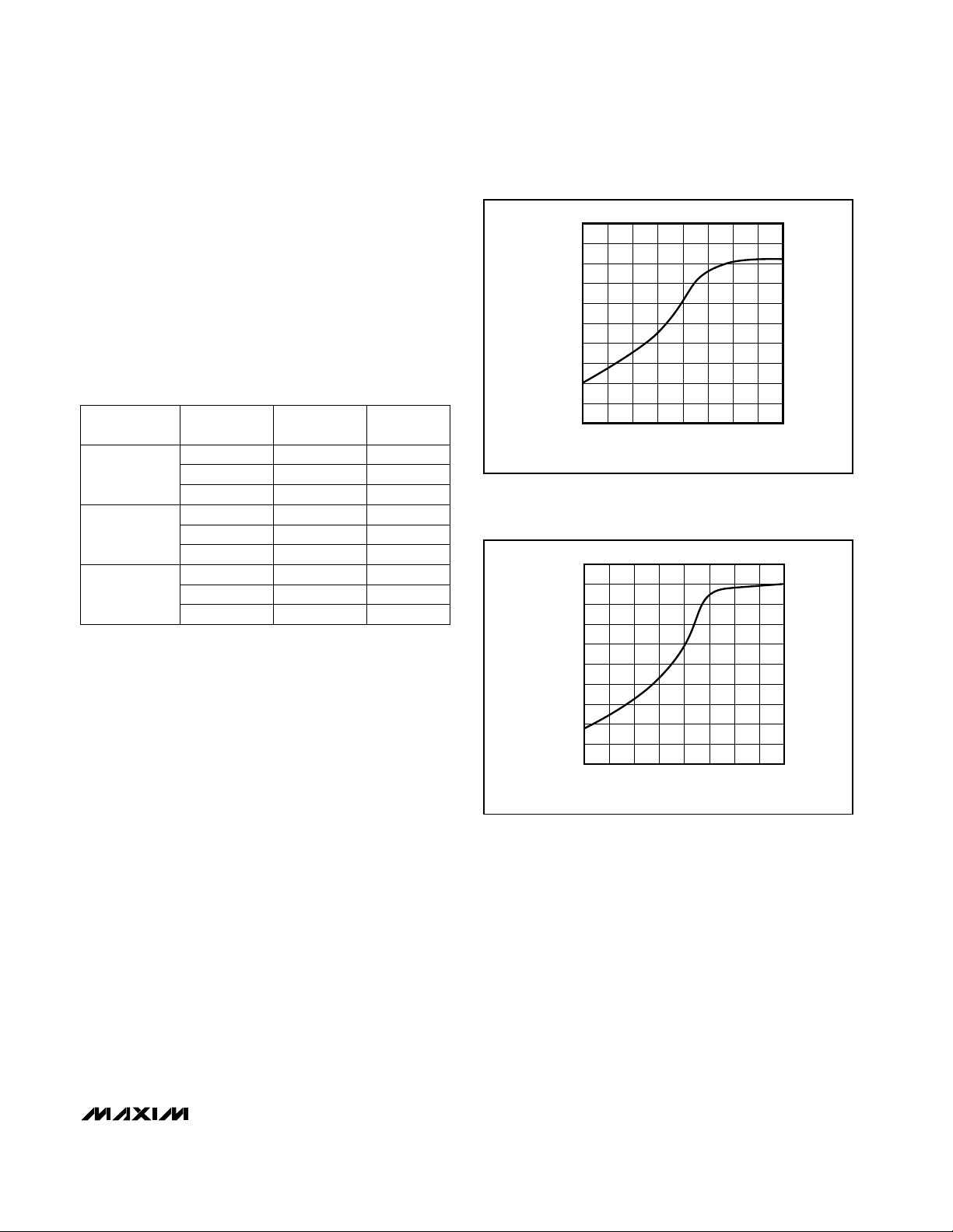
Table 3 lists the possible input-drive combinations for
the mid-gain (250mVp-p) full-scale range selection.
Drive levels are referenced to the open-circuit, common-mode voltage of the analog inputs (typically
2.35V) if DC coupled, or to ground if AC coupling is
used. If the low-gain (500mVp-p) range is selected, the
input-drive requirements are twice those listed in Table
3. If the high-gain (125mVp-p) range is selected, the
input-drive requirements are half those listed in Table 3.
Table 3. Typical Input-Drive Requirements
for Mid-Gain
Offset-Correction Amplifiers
The offset-correction amplifiers included on the
MAX1002 and MAX1003 are usually enabled in a typical AC-coupled application circuit. For DC-coupled
applications, the amplifiers must be disabled by
installing shorting blocks on jumpers JU3, JU4 (I channel); and JU8, JU9 (Q channel). These jumpers short
device pins IOCC+ (pin 2), IOCC- (pin 3), QOCC- (pin
16), and QOCC+ (pin 17) to ground and disable the
amplifiers. The MAX1002/MAX1003 EV kits are configured with the offset-correction amplifiers enabled
(jumpers open) and AC-coupled analog inputs.
Voltage-Controlled-Oscillator Operation
The EV kits include a voltage-controlled-oscillator
(VCO) circuit to set the analog-to-digital converter
(ADC) sampling rate using an external resonant tank
and a varactor diode. A voltage applied to the VTUNE
pad changes the varactor diode’s capacitance to
adjust the tank’s resonant frequency, which sets the
oscillator’s sampling frequency. VTUNE voltage can be
varied from 0V to a maximum of 8V.
The EV kits are designed so that a nominal VTUNE control voltage of about 4V sets the ADC sampling rate to
either 60Msps for the MAX1002 or 90Msps for the
MAX1003. The VTUNE control voltage should be well
filtered, as any noise on the supply contributes to jitter
in the internal oscillator and degrades the converters’
dynamic performance. Figures 1 and 2 show the
VTUNE control-voltage typical frequency-adjustment
ranges for the MAX1002 and MAX1003 EV kits, respectively.
Evaluate: MAX1002/MAX1003
MAX1002/MAX1003 Evaluation Kits
_______________________________________________________________________________________ 3
INPUT DRIVE
Single-Ended
Noninverting
0
+125mV
QIN+ or IIN+
-125mV
Open Circuit
Open Circuit
QIN- or IIN-
Open Circuit
100000
111111
OUTPUT
CODE
000000
Open Circuit
Open Circuit
Open Circuit
0
+125mV
-125mV
Single-Ended
Inverting
011111
000000
111111
0
+62.5mV
-62.5mV
0
-62.5mV
+62.5mV
Differential
100000
111111
000000
Figure 1. MAX1002 Oscillator Frequency vs. VTUNE Control
Voltage
60
70
65
80
75
90
85
95
105
100
110
0 2 31 4 5 6 7 8
MAX100/1003-fig2
VTUNE CONTROL VOLTAGE (V)
FREQUENCY (MHz)
Figure 2. MAX1003 Oscillator Frequency vs. VTUNE Control
Voltage
70
68
66
64
62
60
58
FREQUENCY (MHz)
56
54
52
50
0 2 31 4 5 6 7 8
VTUNE CONTROL VOLTAGE (V)
MAX100/1003-fig1

Evaluate: MAX1002/MAX1003
External Clock Operation
The MAX1002/MAX1003 EV kits can be converted to
drive the ADCs from an external clock source. This
involves removing the external resonator components
from the VCO circuit and adding a few new components. Table 4 lists the EV kit changes required to convert the board to accept an external clock source. The
resulting schematic is shown in Figure 4.
The new 49.9Ω value of R3 shown in Figure 4 provides
proper termination for a 50Ω external signal generator.
AC-coupling capacitor C6 couples the external clock
signal to the MAX1002/MAX1003 oscillator circuitry at
TNK+ (pin 9). R2 and C7 ensure that the impedance at
both ports of the oscillator is balanced. After all modifications are complete, connect an external clock source
to the BNC connector on the EV kit marked CLOCK
OVERDRIVE. The recommended clock amplitude is
1Vp-p; however, the ADC operates correctly with as little as 100mVp-p or up to 2.5Vp-p on CLOCK OVERDRIVE.
The external clock source should have low phase noise
for best dynamic performance. A low-phase-noise
sine-wave oscillator serves this purpose well. A squarewave clock source is not necessary to drive the
MAX1002/MAX1003. The devices contain sufficient
gain to amplify even a low-level-input sine wave to drive
the ADC comparators, while ensuring excellent dynamic performance.
Digital Outputs
The TTL/CMOS-compatible digital outputs are presented in parallel from both I and Q channels at connector
J1. The data format is offset binary with the MSB as D5
and the LSB as D0. The row of pins closest to the
board edge is digital output ground (OGND), while the
data bits occupy the inside row. Located in the middle
of the connector is the pin for the output clock labeled
DCLK. This signal can be used to latch the parallel output data for capture into a logic analyzer or external
DSP circuitry. Both digital outputs are updated on
DCLK’s rising edge (see the timing diagram in the
MAX1002 or MAX1003 data sheet).
_____________Layout Considerations
The MAX1002/MAX1003 EV kit layouts have been optimized for high-speed signals. Careful attention has
been given to grounding, power-supply bypassing, and
signal-path layout to minimize coupling between the
analog and digital sections of the circuit. For example,
the ground plane has been removed under the tank circuitry to reduce stray capacitive loading on the relatively small capacitors required in the external resonant
tank formed by C5, L1, and D1. Other layout considerations are detailed in the following sections.
Power Supplies and Grounding
The EV kits feature separate analog and digital power
supplies and grounds for best dynamic performance. A
thin trace located on the backside of the circuit board
near the VCC power-supply connector ties the analog
and output ground planes together. This trace can be
cut if the power-supply grounds are referenced elsewhere.
Referencing analog and digital grounds together at a
single point usually avoids ground loops and corruption
of sensitive analog circuitry by noise from the digital
outputs. If the ground trace on the backside of the
board is cut, observe the absolute maximum ratings
between the two grounds.
MAX1002/MAX1003 Evaluation Kits
4 _______________________________________________________________________________________
5pF capacitor (MAX1003),
22pF capacitor (MAX1002)
Clock input BNC
connector
DESCRIPTION
47pF capacitors
COMPONENT
Clock Overdrive
C6, C7
C5
Remove
Add
MODIFICATION
Replace with
0.01µF capacitors
10kΩ resistor
220nH inductor
Remove
Remove
47kΩ resistors
Replace with
49.9Ω resistors
L1
R2, R3
R1
Varactor diode RemoveD1
Table 4. External Clock Source EV Kit
Modifications

Bypassing
Proper bypassing is essential to achieve the best
dynamic performance from the converters. The
MAX1002/MAX1003 EV kits use 10µF bypass capacitors located close to the power-supply connectors on
the board to filter low-frequency supply ripple. High-frequency bypassing is accomplished with ceramic chip
capacitors located very close to the device’s supply
pins.
As the digital outputs toggle, transient currents in the
V
CCO
supply can couple into sensitive analog circuitry
and severely degrade the converters’ effective number
of bits performance. Of particular concern is effectively
bypassing V
CCO
to OGND. For best results, locate the
bypass capacitors on the same side of the board and
place them close to the device. This avoids the use of
through-holes and results in lower series inductance.
The capacitor size chosen for the EV kits (size 0603)
keeps the layout compact. Finally, the modest value
(47pF) and small size result in a high self-resonant frequency for effective high-frequency bypassing.
__________Applications Information
To achieve the full dynamic potential from the converters, minimize the capacitive loading on the digital outputs to reduce the transient currents at V
CCO
and
OGND. The maximum capacitance per output bit
should be less than 15pF. For example, the capacitance of the digital output traces and the J1 connector
on the EV kits is about 3pF per trace. In an applications
circuit, this could be further reduced by locating the
digital receiving chip very close to the MAX1002/
MAX1003 and removing the ground plane from under
the output bit traces.
A logic analyzer can be connected to the J1 connector
on the EV kits for evaluation purposes. The analyzer
should be directly connected to the EV kit without any
additional ribbon cables. Even a short length of ribbon
cable can exceed the maximum recommended capacitive loading of the digital outputs. A typical high-speed
logic analyzer probe adds about another 8pF loading
per digital bit, which is acceptable for good dynamic
performance.
Evaluate: MAX1002/MAX1003
MAX1002/MAX1003 Evaluation Kits
_______________________________________________________________________________________ 5

Evaluate: MAX1002/MAX1003
MAX1002/MAX1003 Evaluation Kits
6 _______________________________________________________________________________________
36
35
34
33
32
31
30
29
28
27
26
25
24
23
1
1 3
JU5
2
2
3
4
5
6
7
8
9
10
11
12
13
14
MAX1003
(MAX1002)
22
21
20
19
15
QIN-
V
CC
GND
GND
TNK-
TNK+
VCCGND
VCCIIN-
IIN+
IOCC-
IOCC+
GAIN
IIN+
QIN-
QIN+
BNC
BNC
R4
49.9Ω
R5
49.9Ω
R3
47k
C10
0.01µF
C4
0.22µF
R1
10k
D1
R2
47k
R7
49.9Ω
R6
49.9Ω
VTUNE
VCC
BNC
(22pF)
BNC
= ANALOG GROUND (GND)
= DIGITAL GROUND (OGND)
1
2
3
C8
0.1µF
C9
0.1µF
JU4
VCC
JU3
JU6
0Ω
C13
0.1µF
C1
0.01µF
C3
47pF
C2
47pF
C11
0.01µF
C12
0.01µF
C14
0.1µF
C6
47pF
C7
47pF
C5
5pF
L1
220nH
VCC
JU7
0Ω
IIN-
GND
QOCC+
QOCC-
QIN+
V
CC
DI5
DI4
DI3
DI2
DI1
DQ2
DI0
DCLK
V
CC
OGND
V
CC
DQ0
DQ1
GND
DQ3
DQ4
DQ5
J1–1
J1–3
J1–5
J1–7
J1–9
J1–11
J1–13
JU2
0Ω
JU1
0Ω
VCC
VCCO
J1–15
J1–17
J1–19
J1–21
J1–23
J1–25
J1–4
J1–6
J1–8
J1–10
J1–12
J1–2
J1–16
J1–18
J1–20
J1–22
J1–24
J1–26
J1–14
U1
16
17
18
VTUNE VTUNE
= MAX1002
C16
10µF
VCC
VCCO
JU11
CUT HERE
TO SEPARATE
GROUNDS
JU9
JU8
VCC
GND
VCCO
C15
0.22µF
C17
10µF
OGND
( )
Figure 3. MAX1002/MAX1003 EV Kit Schematic (Voltage-Controlled-Oscillator Mode)

Evaluate: MAX1002/MAX1003
MAX1002/MAX1003 Evaluation Kits
_______________________________________________________________________________________ 7
36
35
34
33
32
31
30
29
28
27
26
25
24
23
1
1 3
JU5
2
2
3
4
5
6
7
8
9
10
11
12
13
14
MAX1003
(MAX1002)
22
21
20
19
15
QIN-
V
CC
GND
GND
TNK-
TNK+
VCCGND
VCCIIN-
IIN+
IOCC-
IOCC+
GAIN
VCC
IIN+
QIN-
QIN+
BNC
BNC
R4
49.9Ω
R5
49.9Ω
C10
0.01µF
C4
0.22µF
R6
49.9Ω
VCC
BNC
BNC
C8
0.1µF
C9
0.1µF
C6
0.01µF
C7
0.01µF
JU4
JU3
0Ω
JU6
C13
0.1µF
C1
0.01µF
C3
47pF
C2
47pF
C11
0.01µF
C12
0.01µF
C14
0.1µF
VCC
JU7
0Ω
IIN-
GND
QOCC+
QOCC-
QIN+
V
CC
DI5
DI4
DI3
DI2
DI1
DQ2
DI0
DCLK
V
CC
OGND
V
CC
DQ0
DQ1
GND
DQ3
DQ4
DQ5
R7
49.9Ω
J1–1
J1–3
J1–5
J1–7
J1–9
J1–11
J1–13
JU2
0Ω
JU1
0Ω
VCC
VCCO
J1–15
J1–17
J1–19
J1–21
J1–23
J1–25
J1–4
J1–6
J1–8
J1–10
J1–12
J1–2
J1–16
J1–18
J1–20
J1–22
J1–24
J1–26
J1–14
BNC
CLK_IN
R3
49.9Ω
R2
49.9Ω
= ANALOG GROUND
= DIGITAL GROUND
U1
16
17
18
VTUNE VTUNE
= MAX1002
C16
10µF
VCC
VCCO
JU11
CUT HERE
TO SEPARATE
GROUNDS
JU9
JU8
VCC
GND
VCCO
C15
0.22µF
OGND
C17
10µF
( )
Figure 4. MAX1002/MAX1003 EV Kit Schematic (External Clock Operation)

Maxim cannot assume responsibility for use of any circuitry other than circuitry entirely embodied in a Maxim product. No circuit patent licenses are
implied. Maxim reserves the right to change the circuitry and specifications without notice at any time.
8
___________________Maxim Integrated Products, 120 San Gabriel Drive, Sunnyvale, CA 94086 (408) 737-7600
© 1997 Maxim Integrated Products Printed USA is a registered trademark of Maxim Integrated Products.
Evaluate: MAX1002/MAX1003
MAX1002/MAX1003 Evaluation Kits
Maxim cannot assume responsibility for use of any circuitry other than circuitry entirely embodied in a Maxim product. No circuit patent licenses are
implied. Maxim reserves the right to change the circuitry and specifications without notice at any time.
8
___________________Maxim Integrated Products, 120 San Gabriel Drive, Sunnyvale, CA 94086 (408) 737-7600
© 1997 Maxim Integrated Products Printed USA is a registered trademark of Maxim Integrated Products.
Figure 5. MAX1002/MAX1003 EV Kit Component Placement
Guide—Component Side
Figure 6. MAX1002/MAX1003 EV Kit Component Placement
Guide—Solder Side
Figure 7. MAX1002/MAX1003 EV Kit PC Board Layout—
Component Side
Figure 8. MAX1002/MAX1003 EV Kit PC Board Layout—
Solder Side
1.0"
1.0"
1.0"
1.0"
 Loading...