

General Description
The MAX328/MA329 are monolithic CMOS analog multiplexers. The MAX328 is a single-ended, 1-of-8 device,
and the MAX329 is a differential, 2-of-8 device.
Designed to provide the lowest possible on- and offleakages, these multiplexers switch signals from high
source impedance, providing the mux operates into a
high-input-impedance op amp or A/D converter. The
MAX328/MAX329 are pin-for-pin replacements for the
popular DG508/DG509 in these applications.
Adding an external 40kΩ resistor to each input makes
the MAX328/MAX329 an excellent fault-tolerant multiplexer. Low leakage (less than 1pA at +25°C) and
2.5kΩ on-resistance allow the circuit to sustain 110V
AC faults indefinitely while maintaining an error of less
than 40nV for normal signals (i.e., 1pA times 40kΩ).
The MAX328/MAX329 work equally well with a single
supply of 10V to 30V or dual supplies of ±5V to ±18V.
They also perform well with unbalanced combinations of
supply voltage, such as +12V and -5V or +5V and -15V.
Low power dissipation (1.9mW with ±15V supplies)
allows use in portable applications.
Applications
Control Systems
Data Logging Systems
Aircraft Heads-Up Displays
Data-Acquisition Systems
Signal Routing
Features
♦ Ultra-Low Off- and On-Leakage: 1pA Typ
♦ Bidirectional Operation (Use as Mux or Demux)
♦ TTL and CMOS Logic Compatibility
♦ Analog Signal Range Includes Power-Supply Rails
♦ Switching Speeds Less Than 1.5µs
♦ Pin Compatible with DG508/DG509 and
MAX358/MAX359
♦ Latchup Proof Construction
MAX328/MAX329
Ultra-Low Leakage Monolithic CMOS
Analog Multiplexers
________________________________________________________________ Maxim Integrated Products 1
Pin Configurations
Ordering Information
MAX328
V+ V-GND
A
0A1A2
EN
S1
S8
D
OP
AMP
+15V -15V
40kΩ
1/2W
40kΩ
1/2W
ANALOG
INPUT
ANALOG
INPUT
DM7493
+15V
+15V
N.C.
CLK IN
N.C.
GNDV
02V01
AIN
BIN
Q
B
Q
C
Q
O
Q
A
V+
EN IN
(MUX ON/OFF CONTROL)
OUT
i BIAS < 1pA
1-OF-8 CHANNEL SEQUENTIAL MUX WITH 120V AC FAULT CAPABILITY
Typical Operating Circuit
19-1006; Rev 2; 9/01
For pricing, delivery, and ordering information, please contact Maxim/Dallas Direct! at
1-888-629-4642, or visit Maxim’s website at www.maxim-ic.com.
*Contact factory for dice specifications.
**Contact factory for availability. Substrate may be allowed to
float or be connected to V+.
Ordering Information and Pin Configurations continued at
end of data sheet.
PART TEMP RANGE PIN-PACKAGE
MAX328CPE 0°C to +70°C 16 Plastic DIP
MAX328CWE 0°C to +70°C 16 Wide SO
MAX328CJE 0°C to +70°C 16 CERDIP
MAX328C/D 0°C to +70°C Dice*
MAX328EGE -40°C to +85°C 16 QFN
MAX328EPE -40°C to +85°C 16 Plastic DIP
MAX328EWE -40°C to +85°C 16 Wide SO
MAX328EJE -40°C to +85°C 16 CERDIP**
MAX328MJE -55°C to +125°C 16 CERDIP**
TOP VIEW
A0
1
2
EN
V-
3
MAX328
4
S1
S2
5
S3
6
S4
7
D
8
A0
1
EN
2
V-
3
MAX329
4
S1A
S2A
5
S3A
6
S4A
7
DA
8
DIP/SO
DIP/SO
16
A1
15
A2
14
GND
13
V+
12
S5
S6
11
10
S7
9
S8
16
A1
15
GND
14
V+
13
S1B
12
S2B
S3B
11
10
S4B
9
DB
MAX328/MAX329
Ultra-Low Leakage Monolithic CMOS
Analog Multiplexers
2 _______________________________________________________________________________________
ABSOLUTE MAXIMUM RATINGS
ELECTRICAL CHARACTERISTICS
(V+ = +15V, V- = -15V, GND = 0V, TA= +25°C, unless otherwise noted.)
Stresses beyond those listed under “Absolute Maximum Ratings” may cause permanent damage to the device. These are stress ratings only, and functional
operation of the device at these or any other conditions beyond those indicated in the operational sections of the specifications is not implied. Exposure to
absolute maximum rating conditions for extended periods may affect device reliability.
Voltage Referenced to V-
V+ ........................................................................................+44V
GND .....................................................................................+25V
Digital Inputs (Note 1), V
S
, VD............................-2V to (V+ + 2V)
Current (Any Terminal, Except S or D)................................30mA
Continuous Current, S or D
(pulsed at 1ms, 10% duty cycle max) ............................40mA
Operating Temperature Range
MAX328/329 C _ _ ..............................................0°C to +70°C
MAX328/329 E _ _ ...........................................-40°C to +85°C
MAX328/329 M _ _.........................................-55°C to +125°C
Power Dissipation (Package) (Note 1)
16-Pin CERDIP (Note 2) ...............................................900mW
16-Pin Plastic DIP (Note 3)...........................................470mW
16-Pin Wide SO (Note 4) ..............................................750mW
16-Pin QFN (Note 5) ...................................................1538mw
Storage Temperature.........................................-65°C to +150°C
)
)
Note 1: All leads soldered or welded to PC board.
Note 2: Derate 12mW/°C above +75°C.
Note 3: Derate 6.3mW/°C above +75°C.
Note 4: Derate 10mW/°C above +75°C.
Note 5: Derate 19.2mW/°C above +75°C.
PARAMETER SYMBOL TEST CONDITIONS
SWITCH
Analog Signal Range V
Drain-Source
On-Resistance
Greatest Change in
Drain-Source OnResistance Between
Channels
Source Off-Leakage
Current (Note 6)
Drain OffLeakage
Current (Note 6)
Drain OnLeakage
Current (Note 6)
MAX328
MAX329
MAX328
MAX329
ANALOG
R
DS(ON
∆R
DS(ON
I
S(OFF)
I
D(OFF)
I
D(ON)
VD = 10V,
= 100µA
I
S
VD = -10V,
= 100µA
I
S
R
=
DS(on)
R
(
R
VS = 10V, VD = -10V 0.1 ±10 0.1 ±10
VS = -10V, VD = 10V
VD = 10V, VS = -10V 0.3 ±10 0.3 ±10
V
D
VD = 10V, VS = -10V 0.3 ±10 0.3 ±10
VD = -10V, VS = 10V
VS (all) = VD = 10V 3.0 ±10 3.0 ±10
V
S
VS (all) = VD = 10V 1.5 ±10 1.5 ±10
VS (all) = VD = -10V
Max - R
DS(ON)
= -10V, VS = 10V 1.0 ±10 1.0 ±10
(all) = VD = -10V 2.0 ±10 2.0 ±10
DS(ON)
DS(ON)
Ave
LIMITS
Seq. each
switch on,
= 0.8V,
V
AL
= 2.4V
V
AH
Min
)
= 0V
V
EN
V
= 0V
EN
Seq. each
switch on,
= 0.8V,
V
AL
V
= 2.4V
AH
MAX328M
MAX329M
MIN TYP MAX MIN TYP MAX
±15 ±15 V
1.5 2.5 1.5 3.5
1.0 2.5 1.0 3.5
22%
0.3 ±10 0.3 ±10
0.5 ±10 0.5 ±10
1.0 ±10 1.0 ±10
MAX328C/E
MAX329C/E
UNITS
kΩ
pA
pA
pA
MAX328/MAX329
Ultra-Low Leakage Monolithic CMOS
Analog Multiplexers
_______________________________________________________________________________________ 3
ELECTRICAL CHARACTERISTICS (continued)
(V+ = +15V, V- = -15V, GND = 0V, TA= +25°C, unless otherwise noted.)
)
)
)
)
Note 6: All leakage parameters are 100% tested at maximum rated operating temperature, i.e., +70°C, +85°C, +125°C, and guaran-
teed by correlation at +25°C.
Note 7: Electrical characteristics, such as On-Resistance, change when power supplies other than ±15V are used. Power-supply
range is a design characteristic, not production tested.
Note 8: Guaranteed by design.
Typical values are for DESIGN AID ONLY, not guaranteed or subject to production testing.
PARAMETER SYMBOL TEST CONDITIONS
INPUT
Address Input Current,
Input Voltage High
Address Input Current,
Input Voltage Low
DYNAMIC
Switching Time of
Multiplexer
Break-Before-Make
Interval
Enable Turn-On Time t
Enable Turn-Off Time t
Off-Isolation OIRR
Source Off-Capacitance C
Drain OffCapacitance
Charge Injection (Note 8)
SUPPLY
Positive Supply Current I+ VEN = 2.4V VA = 0V/5V 4.5 200 4.5 200 µA
Negative Supply Current I- VEN = 2.4V VA = 0V/5V 1 -100 1 -100 µA
Power-Supply Range for
Continuous Operation
(Note 7)
MAX328 8.0 8.0
MAX329
I
AH
I
AL
t
TRANSITION
t
OPEN
ON(EN
OFF(EN
S(OFF
C
D(OFF
Q
(INJ)
V
OP
VA = 2.4V 0.001 ±1 0.001 ±1
VA = 15V 0.001 ±1 0.001 ±1
VEN = 2.4V 0.001 ±1 0.001 ±1
VEN = 0V
See Figure 1 1.0 1.5 µs
See Figure 2 0.2 0.2 µs
See Figure 3 1.0 1.5 µs
See Figure 3 0.7 1.0 µs
V
= 0V, RL = 1kΩ, CL = 15pF,
EN
V
= 7V
S
VS = 0V
VD = 0V
VA = +10V 1 1
VA = 0V 2 5 2 5
VA = -10V 4 4
, f = 500kHz
RMS
All
V
= 0V
A
V
= 0V,
EN
f = 1MHz
V
= 0V,
EN
f = 1MHz
MAX328M
MAX329M
MIN TYP MAX MIN TYP MAX
0.001 ±1 0.001 ±1
84 84 dB
1.8 1.8 pF
4.0 4.0
±5 ±18 ±5 ±18 V
LIMITS
MAX328C/E
MAX329C/E
UNITS
µA
µA
pF
pc

MAX328/MAX329
Ultra-Low Leakage Monolithic CMOS
Analog Multiplexers
4 _______________________________________________________________________________________
ELECTRICAL CHARACTERISTICS (Over Temperature)
(V+ = +15V, V- = -15V, GND = 0V, TA= T
MIN
to T
MAX
, unless otherwise noted.)
)
Note 9: Leakage parameters are 100% tested at maximum rated operating temperature, i.e., +70°C, etc.
PARAMETER SYMBOL TEST CONDITIONS
SWITCH
Analog Signal Range V
Drain-Source
On-Resistance
Source OffLeakage Current (Note 9)
Drain OffLeakage
Current (Note 9)
Drain OnLeakage
Current (Note 9)
INPUT
Address Input Current,
Input Voltage High
Address Input Current,
Input Voltage Low
MAX328
MAX329
MAX328
MAX329
ANALOG
R
DS(ON
I
S(OFF)
I
D(OFF)
I
D(ON)
I
AH
I
AL
VD = 10V,
= 100µA
I
S
VD = -10V,
= 100µA
I
S
VS = 10V, VD = -10V ±5 ±5
VS = -10V, VD = 10V
VD = 10V, VS = -10V ±20 ±20
= -10V, VS = 10V ±20 ±20
V
D
VD = 10V, VS = -10V ±10 ±10
VD = -10V, VS = 10V
VS (all) = VD = 10V ±20 ±20
(all) = VD = -10V ±20 ±20
V
S
VS (all) = VD = 10V ±10 ±10
VS (all) = VD = -10V
VA = 2.4V 0.01 ±1 0.01 ±1
VA = 15V 0.01 ±1 0.01 ±1
VEN = 2.4V 0.01 ±1 0.01 ±1
VEN = 0V
Seq. each
switch on,
V
AL
V
AH
V
EN
V
EN
Seq. each
switch on,
V
AL
V
AH
All
V
= 0V
A
= 0.8V,
= 2.4V
= 0V
= 0V
= 0.8V,
= 2.4V
MAX328M
MAX329M
MIN TYP MAX MIN TYP MAX
±15 ±15 V
2.2 4 1.9 5
1.5 4 1.2 5
0.01 ±1 0.01 ±1
LIMITS
MAX328C/E
MAX329C/E
±5 ±5
±10 ±10
±10 ±10
UNITS
kΩ
nA
nA
nA
µA
µA

MAX328/MAX329
Ultra-Low Leakage Monolithic CMOS
Analog Multiplexers
_______________________________________________________________________________________ 5
Typical Operating Characteristics
(TA = +25°C, unless otherwise noted.)
R
DS(ON)
vs. ANALOG INPUT
FOR DUAL SUPPLIES
MAX328/MAX329 toc01
ANALOG INPUT (V)
R
DS(ON)
(kΩ)
1050-5-10
1
2
3
4
5
6
7
8
9
0
-15 15
±5V SUPPLIES
±15V SUPPLIES
R
DS(ON)
vs. ANALOG INPUT
FOR SINGLE SUPPLY
MAX328/MAX329 toc02
ANALOG INPUT (V)
R
DS(ON)
(kΩ)
105
1
2
3
4
5
0
015
WITH +15V SUPPLY
I
S(OFF)
vs. TEMPERATURE
MAX328/MAX329 toc03
TEMPERATURE (°C)
LEAKAGE (nA)
105856545255-15-35
0.001
0.01
0.1
1.0
10.0
0.0001
-55 125
V+ = 15V
V- = 15V
MAX328/
MAX329
I
D(ON), ID(OFF)
vs. TEMPERATURE
MAX328/MAX329 toc04
TEMPERATURE (°C)
LEAKAGE (nA)
105856545255-15-35
0.01
0.1
1.0
10
100
0.001
-55 125
V+ = 15V
V- = 15V
MAX328

MAX328/MAX329
Ultra-Low Leakage Monolithic CMOS
Analog Multiplexers
6 _______________________________________________________________________________________
Pin Description
Truth Table—MAX328
Truth Table—MAX329
Note: Logic “0” = VAL≤ 0.8V, Logic “1” = VAH≥ 2.4V
PIN
MAX328 MAX329
DIP/SO QFN DIP/SO QFN
1, 15, 16 15, 14, 13 ——A0, A2, A1 Address Input
——1, 16 15, 14 A0, A1 Address Input
2 16 2 16 EN Enable
3 1 3 1 V- Negative-Supply Voltage Input
4–72–5 ——S1–S4 Analog Inputs—Bidirectional
——4–72–5 S1A–S4A Analog Inputs—Bidirectional
86—— D Analog Outputs—Bidirectional
——8, 9 6, 7 DA, DB Analog Outputs—Bidirectional
9–12 7–10 ——S8–S5 Analog Inputs—Bidirectional
——10–13 8–11 S4B–S1B Analog Inputs—Bidirectional
13 11 14 12 V+ Positive-Supply Voltage Input
14 12 15 13 GND Ground
A
2
X X X 0 None
00001
00112
01013
01114
10015
10116
11017
11118
A
1
A
0
EN
SWITCH
NAME FUNCTION
ON
A
1
X X 0 None
0011
0112
1013
1114
A
0
EN
ON
SWITCH

MAX328/MAX329
Ultra-Low Leakage Monolithic CMOS
Analog Multiplexers
_______________________________________________________________________________________ 7
Figure 2. Break-Before-Make Delay (t
OPEN
)
Figure 3. Enable Delay (t
ON(EN)
, t
OFF(EN)
)
Figure 1. Access Time vs. Logic Level (High)
VAH = 3.0V
50%
+10V
90%
t
A
V
0V
AH
ADDRESS
DRIVE (V
OUTPUT A
-10V
= 3.0V
ADDRESS
DRIVE (V
OUTPUT
50%50%
1kΩ
±10V
±
10V
10MΩ
PROBE
14pF
12.5pF
+5V
V
OUT
A
2
)
A
0V
V
A
50Ω
+V
V
)
A
A
50Ω
2.4V
A
1
A
0
EN
AH
A
2
A
1
A
0
EN
MAX328
GND
MAX328
GND
S2–S
S2–S
OUT
OUT
S
S
S
1
S
2
7
S
8
1
7
8
t
OPEN
V
= 3.0V
AH
50%
90%
t
ON(EN)
ENABLE DRIVE
t
OFF(EN)
0V
OUTPUT
90%
1kΩ
+10V
12.5pF
A
2
A
1
A
0
EN
V
A
50Ω
MAX328
GND
S2–S
OUT
S
1
7
MAX328/MAX329
Ultra-Low Leakage Monolithic CMOS
Analog Multiplexers
8 _______________________________________________________________________________________
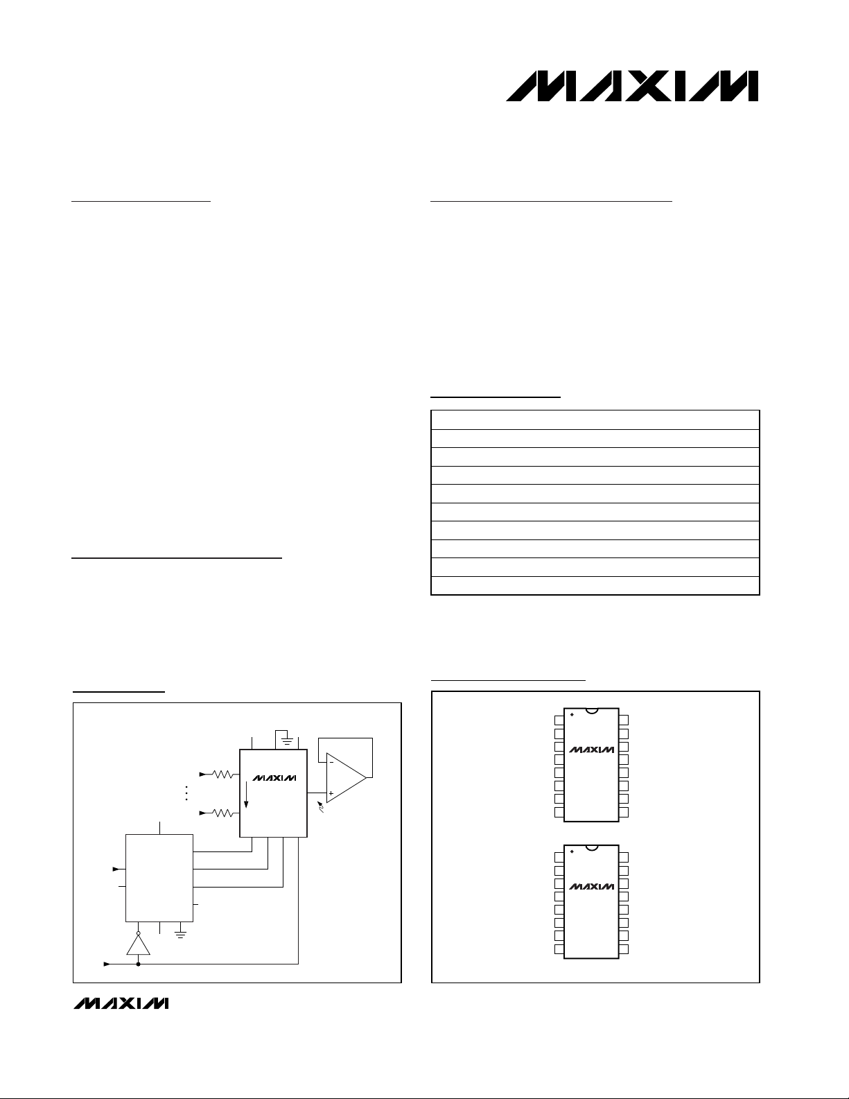
Applications Information
Figure 4 is a typical circuit for converting the
MAX328/MAX329 into a fault-tolerant mux. In this
application, the internal diodes limit the voltage at the
MAX328 input to ±15.7V (±15V supplies). No external
diodes need to be added with the MAX328/MAX329,
unlike conventional multiplexers requiring external
diodes.
The resistors, R, need to be 39kΩ or higher to limit the
power dissipation in the resistor when a 120V AC fault
occurs (i.e., power dissipation is (120-16)2/39kΩ or
0.28W. This is why a 1/2/W resistor is needed). The circuit
withstands an indefinite fault to a 120V AC line with no
damage to any component.
In addition to allowing fault-protection, the guaranteed
low leakage of the MAX328/MAX329 also reduces signal
errors. The circuit in Figure 4 produces an error voltage of
10pA (max leakage) x 39kΩ or 0.39µV at room temperature and 39µV at +125°C. Therefore, for 10V signals, the
MAX328/MAX329 allows 17-bit resolution (38µV = 1LSB)
over the full temperature range.
S8 D
98
10
11
12
13
14
S7
S6
S5
V+
GND
7
6
5
4
3
S4
S3
S2
S1
V-
15 16 1 2
A2 A1 A0 EN
0.104”
(2.64mm)
0.118”
(2.90mm)
0.104”
(2.64mm)
0.118”
(2.90mm)
ENA0A1
2116
7
6
5
4
3
S4A
S3A
S2A
S1A
V-
DB DA
98
10
11
12
13
14
15
S4B
S3B
S2B
S1B
V+
GND
MAX328
MAX329
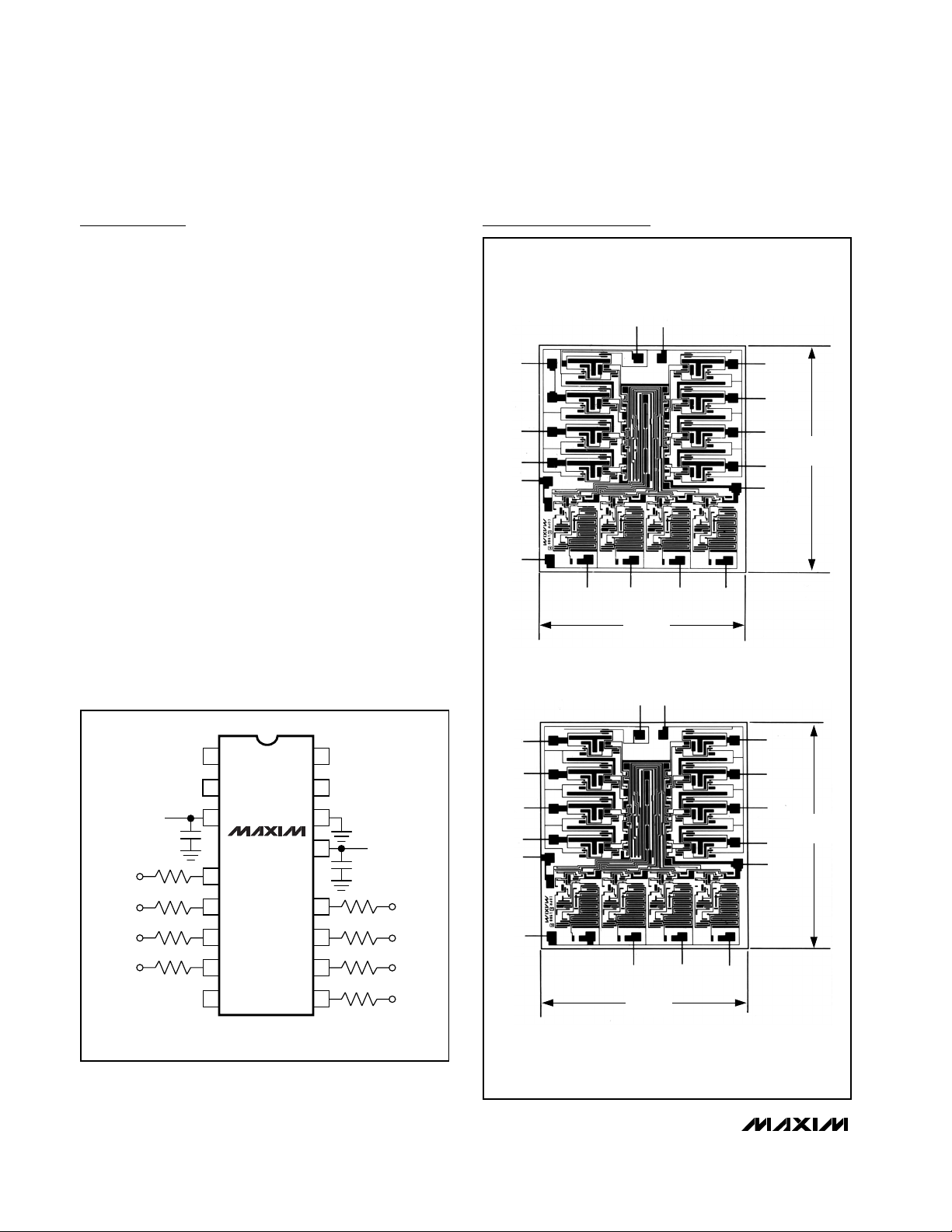
Chip Topographies
Figure 4. Fault-Tolerant MUX (indefinitely withstands 120V AC
fault voltages)
A
0
1
EN
2
16
A
1
A
15
2
-15V
1µF
S
1
S
2
S
3
S
4
R = 39kΩ 1/2W
R
R
R
R
V
OUT
3
MAX328
MAX329
4
5
6
7
8
14
13
12
11
10
9
1µF
R
R
R
R
+15V
S
5
S
6
S
7
S
8

MAX328/MAX329
Ultra-Low Leakage Monolithic CMOS
Analog Multiplexers
Maxim cannot assume responsibility for use of any circuitry other than circuitry entirely embodied in a Maxim product. No circuit patent licenses are
implied. Maxim reserves the right to change the circuitry and specifications without notice at any time.
Maxim Integrated Products, 120 San Gabriel Drive, Sunnyvale, CA 94086 408-737-7600 _____________________ 9
© 2001 Maxim Integrated Products Printed USA is a registered trademark of Maxim Integrated Products.
Ordering Information (continued)
*Contact factory for dice specifications.
**Contact factory for availability. Substrate may be allowed to
float or be connected to V+.
Pin Configurations (continued)
Package Information
For the latest package outline information, go to
www.maxim-ic.com/packages
.
PART TEMP RANGE PIN-PACKAGE
MAX329CPE 0°C to +70°C 16 Plastic DIP
MAX329CWE 0°C to +70°C 16 Wide SO
MAX329CJE 0°C to +70°C 16 CERDIP
MAX329C/D 0°C to +70°C Dice*
MAX329EGE -40°C to +85°C 16 QFN
MAX329EPE -40°C to +85°C 16 Plastic DIP
MAX329EWE -40°C to +85°C 16 Wide SO
MAX329EJE -40°C to +85°C 16 CERDIP**
MAX329MJE -55°C to +125°C 16 CERDIP**
TOP VIEW
16 EN
15 A0
14 A1
13 A2
1V-
2S1
3S2
4S3
1V-
2S1A
3S2A
4S3A
5S4
16 EN
5S4A
LOGIC
6D
MAX328
15 A0
LOGIC
6DA
7S88S7
14 A1
13 GND
7DB8S4B
12 GND
11 V+
10 S5
9S6
12 V+
11 S1B
10 S2B
9 S3B
MAX329
 Loading...