

Page 1
General Description
The LM75 temperature sensor includes a delta-sigma
analog-to-digital converter, and a digital overtemperature detector. The host can query the LM75 through its
I2C interface to read temperature at any time. The
open-drain overtemperature output (OS) sinks current
when the programmable temperature limit is exceeded.
The OS output operates in either of two modes, comparator or interrupt. The host controls the temperature
at which the alarm is asserted (TOS) and the hysteresis
temperature below which the alarm condition is not
valid (T
HYST
). Also, the LM75’s TOSand T
HYST
registers can be read by the host. The address of the LM75
is set with three pins to allow multiple devices to work
on the same bus. Power-up is in comparator mode, with
defaults of TOS= +80°C and T
HYST
= +75°C. The 3.0V
to 5.5V supply voltage range, low supply current, and
I2C interface make the LM75 ideal for many applications in thermal management and protection.
Applications
Thermal System Management
Thermal Protection
Test Equipment
Computers and Office Electronics
Features
♦ SO (SOP) and µMAX®(µSOP) Packages
♦ I2C Bus Interface
♦ Separate Open-Drain OS Output Operates as
Interrupt or Comparator/Thermostat Input
♦ Register Readback Capability
♦ Power-Up Defaults Permit Stand-Alone Operation
as a Thermostat
♦ 3.0V to 5.5V Supply Voltage
♦ Low Operating Supply Current 250µA (typ), 1mA
(max)
♦ 4µA (typ) Shutdown Mode Minimizes Power
Consumption
♦ Up to Eight LM75s Can Be Connected to a Single
Bus
♦ Pin- and/or Register-Compatible with Improved-
Performance Maxim Sensors Including MAX7500,
MAX6625, MAX6626, DS75LV, and DS7505
LM75
Digital Temperature Sensor and Thermal
Watchdog with 2-Wire Interface
________________________________________________________________
Maxim Integrated Products
1
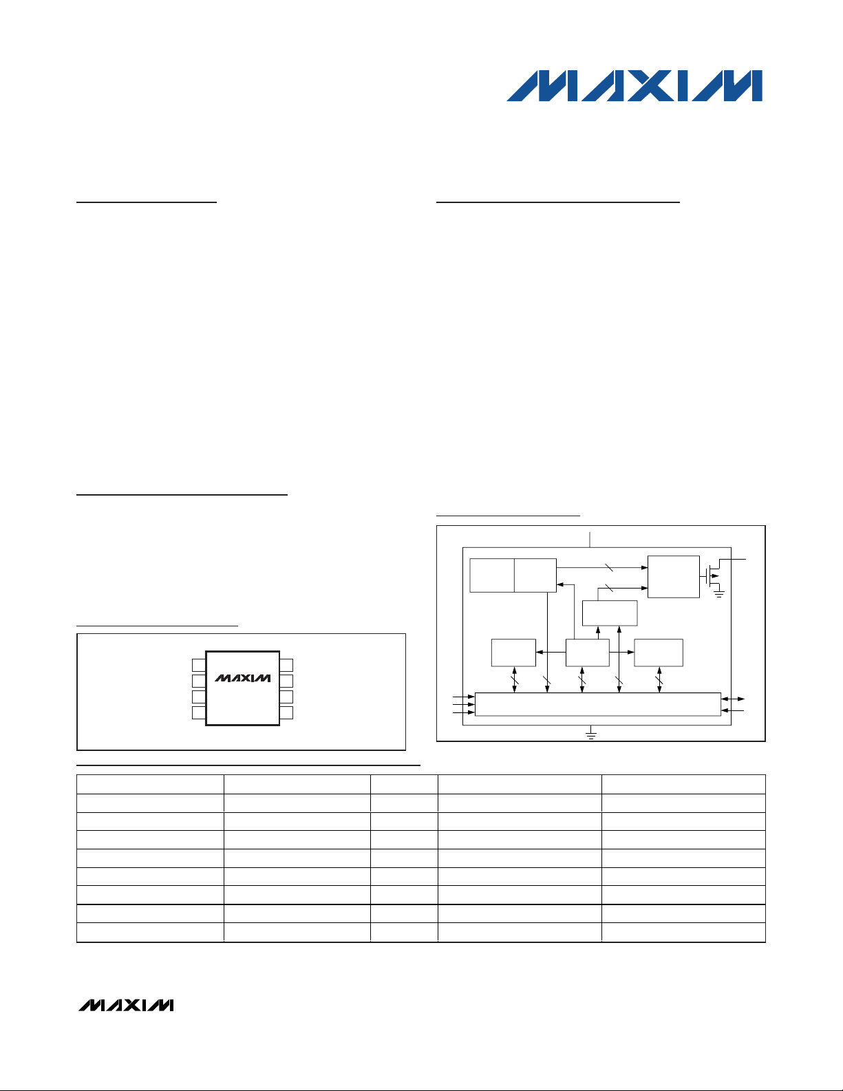
Functional Diagram
Ordering Information/Selector Guide
19-4385; Rev 0; 3/09
For pricing, delivery, and ordering information, please contact Maxim Direct at 1-888-629-4642,
or visit Maxim’s website at www.maxim-ic.com.
µMAX is a registered trademark of Maxim Integrated Products, Inc.
Note: Devices are specified over the -55°C to +125°C temperature range and include I
2
C noise filter.
+
Denotes a lead(Pb)-free/RoHS-compliant package.
T&R = Tape and reel.
Pin Configuration
TOP VIEW
+
SDA
1
2
SCL
3
OS
4
μMAX (μSOP), SO
LM75
8
+V
S
7
A0
6
A1
5
A2GND
= 3.0V to 5.5V
+V
S
8
SILICON
9-BIT DELTA-
BANDGAP
TEMPERATURE
7
A0
6
A1
5
A2
SIGMA ADC
SENSOR
CONFIGURATION
REGISTER
8816 16 16
16
16
TOS SET POINT
REGISTER
POINTER
REGISTER
2-WIRE INTERFACE
4
SET POINT
COMPARATOR W/
HYSTERESIS
SET
T
HYST
POINT REGISTER
3
1
2
OS
SDA
SCL
PART PIN-PACKAGE PKG SUPPLY VOLTAGE (V) TOP MARK
LM75BIM-3+ 8 SO (SOP) Bulk 3.3 LM75BIM-3
LM75BIMX-3+ 8 SO (SOP) T&R 3.3 LM75BIM-3
LM75BIMM-3+ 8 µMAX (µSOP) Bulk 3.3 T01B
LM75BIMMX-3+ 8 µMAX (µSOP) T&R 3.3 T01B
LM75BIM-5+ 8 SO (SOP) Bulk 5.0 LM75BIM-5
LM75BIMX-5+ 8 SO (SOP) T&R 5.0 LM75BIM-5
LM75BIMM-5+ 8 µMAX (µSOP) Bulk 5.0 T00B
LM75BIMMX-5+ 8 µMAX (µSOP) T&R 5.0 T00B
Page 2
LM75
Digital Temperature Sensor and Thermal
Watchdog with 2-Wire Interface
2 _______________________________________________________________________________________
ABSOLUTE MAXIMUM RATINGS (Note 1)
ELECTRICAL CHARACTERISTICS
(+VS= +3.0V to +5.5V, unless otherwise noted. Temperature accuracy specifications apply for +VS= 3.3V for versions with “-3” in
the suffix and for +V
S
= 5V for versions with “-5” in the suffix. TA= -55°C to +125°C, unless otherwise noted. Typical values are at
+V
S
= +5V, TA= +25°C.) (Notes 4, 5)
Stresses beyond those listed under “Absolute Maximum Ratings” may cause permanent damage to the device. These are stress ratings only, and functional
operation of the device at these or any other conditions beyond those indicated in the operational sections of the specifications is not implied. Exposure to
absolute maximum rating conditions for extended periods may affect device reliability.
+VSto GND ...........................................................-0.3V to +6.0V
OS, SDA, SCL to GND...........................................-0.3V to +6.0V
All Other Pins to GND.................................-0.3V to (+V
S
+ 0.3V)
Input Current at Any Pin (Note 2)..........................................5mA
Package Input Current (Note 2)..........................................20mA
OS Output Sink Current ......................................................10mA
Continuous Power Dissipation (T
A
= +70°C) (Note 3)
8-Pin µMAX (µSOP)
(derate 4.5mW/°C above +70°C)..................................362mW
8-Pin SO (SOP) (derate 5.9mW/°C above +70°C) ........471mW
Junction-to-Case Thermal Resistance (θ
JC
) (Note 3)
8-Pin µMAX (µSOP).......................................................42°C/W
8-Pin SO (SOP)..............................................................40°C/W
Junction-to-Ambient Thermal Resistance (θ
JA
) (Note 3)
8-Pin µMAX (µSOP).....................................................221°C/W
8-Pin SO (SOP)............................................................170°C/W
ESD Protection
Human Body Model (R
D
= 1.5kΩ, CS= 100pF)
All Pins to GND .................................................................±2kV
Operating Temperature Range .........................-55°C to +125°C
Junction Temperature......................................................+150°C
Storage Temperature Range .............................-65°C to +150°C
Lead Temperature (soldering, 10s) .................................+300°C
Note 1: Absolute Maximum Ratings indicate limits beyond which damage to the device may occur. DC and AC electrical specifica-
tions do not apply when operating the device beyond its rated operating conditions.
Note 2: When the input voltage (V
I
) at any pin exceeds the Absolute Maximum Ratings limits (VI< GND, VI> 6V or VI> +VS), the
current at that pin should be limited to 5mA. The 20mA maximum package input current rating limits the number of pins that
can safely exceed the power supplies with an input current of 5mA to four.
Note 3: Package thermal resistances were obtained using the method described in JEDEC specification JESD51-7, using a single-
layer board. For detailed information on package thermal considerations, refer to www.maxim-ic.com/thermal-tutorial
.
Accuracy (Six-Sigma)
Accuracy (Three-Sigma) (Note 6)
Resolution 9 Bits
Temperature Conversion Time (Note 7) 100 300 ms
Quiescent Supply Current
+VS Supply Voltage Range 3.0 5.5 V
OS Output Saturation Voltage I
OS Delay (Note 9) 1 6
OS Output Fall Time t
TOS Default Temperature (Note 11) 80 °C
T
HYST
PARAMETER SYMBOL CONDITIONS MIN TYP MAX UNITS
Default Temperature (Note 11) 75 °C
-25°C ≤ TA ≤ +100°C -2.0 +2.0
≤ +125°C -3.0 +3.0
A
≤ +125°C -2.0 +2.0
A
= 5V 6
S
= 4.0mA (Note 8) 0.8 V
Conver-
sions
OF
-55°C ≤ T
-25°C ≤ TA ≤ +100°C -1.5 +1.5
-55°C ≤ T
I2C inactive 0.25 0.5 mA
Shutdown mode, +VS = 3V 4
Shutdown mode, +V
OUT
CL = 400pF, IO = 3mA (Note 10) 250 ns
°C
°C
µA
Page 3
LM75
Digital Temperature Sensor and Thermal
Watchdog with 2-Wire Interface
_______________________________________________________________________________________ 3
ELECTRICAL CHARACTERISTICS (continued)
(+VS= +3.0V to +5.5V, unless otherwise noted. Temperature accuracy specifications apply for +VS= 3.3V for versions with “-3” in
the suffix and for +V
S
= 5V for versions with “-5” in the suffix. TA= -55°C to +125°C, unless otherwise noted. Typical values are at
+V
S
= +5V, TA= +25°C.) (Notes 4, 5)
Note 4: All parts operate properly over the 3V to 5.5V supply voltage range. The devices are tested and specified for rated
accuracy at their nominal supply voltage.
Note 5: All parameters are measured at T
A
= +25°C. Values over the temperature range are guaranteed by design.
Note 6: There is no industry-wide standard for temperature accuracy specifications. Maxim’s standard is six-sigma. The three-
sigma specification is included to allow easier comparison to products built by manufacturers who use different standards.
Note 7: This specification indicates how often temperature data is updated. The devices can be read at any time without regard to
conversion state, while yielding the last conversion result.
Note 8: For best accuracy, minimize output loading. Higher sink currents can affect sensor accuracy due to internal heating.
Note 9: OS delay is user programmable up to 6 over-limit conversions before OS is set to minimize false tripping in noisy environ-
ments.
Note 10: Guaranteed by design.
Note 11: Default values set at power-up.
Note 12: All timing specifications are guaranteed by design.
Note 13: Unless otherwise noted, these specifications apply for +V
S
= +5VDC for LM75BIM-5 and LM75BIMM-5 and +VS=
+3.3VDC for LM75BIM-3 and LM75BIMM-3. C
L
(load capacitance) on output lines = 80pF, unless otherwise specified.
The switching characteristics of the LM75 fully meet or exceed the published specifications of the I2C bus. These parameters are the timing relationships between SCL and SDA signals related to the LM75. They are not I
2
C bus specifications.
Note 14: Holding the SDA line low for a time greater than t
TIMEOUT
causes the device to reset SDA to the IDLE state of the
serial bus communication (SDA set high).
LOGIC (SDA, SCL, A0, A1, A2)
Input High Voltage V
Input Low Voltage V
Input High Current I
Input Low Current I
Input Capacitance C
Output High Current VOH = 5V 10 µA
Output Low Voltage IOL = 3mA 0.4 V
I2C-COMPATIBLE TIMING (Notes 12, 13)
(Clock) SCL Period t
Data In Setup Time to SCL High t
Data Out Stable After SCL Low t
Start Condition Setup Time
(SDA Low to SCL Low)
STOP Condition Hold Time t
SDA Time Low for Reset of Serial
Interface
PARAMETER SYMBOL CONDITIONS MIN TYP MAX UNITS
IH
IL
IH
IL
IN
SCL
SU:DAT
HD:DAT
t
SU:STA
HD:STO
t
TIMEOUT
+VS x
0.7
-0.3
VIN = 5V 0.005 1.0 µA
VIN = 0V -1.0 -0.005 µA
All digital inputs 20 pF
Bus timeout inactive 2.5 µs
10% of SDA to 10% of SCL 100 ns
10% of SCL to 10% of SDA 0 µs
90% of SCL to 90% of SDA 100 ns
100 ns
(Note 14) 75 325 ms
+VS +
0.5
+V
S
0.3
x
V
V
Page 4
QUIESCENT SUPPLY CURRENT
vs. TEMPERATURE
LM75 toc01
TEMPERATURE (°C)
QUIESCENT SUPPLY CURRENT (μA)
9565355-25
240
250
260
270
280
290
300
230
-55 125
+VS = +5V
+VS = +3V
SHUTDOWN SUPPLY CURRENT (μA)
1
2
3
4
5
6
0
SHUTDOWN SUPPLY CURRENT
vs. TEMPERATURE
LM75 toc02
TEMPERATURE (°C)
9565355-25-55 125
+VS = +5V
+VS = +3V
ACCURACY vs. TEMPERATURE
ACCURACY (°C)
-1.5
-1.0
-0.5
0
0.5
1.0
1.5
2.0
-2.0
LM75 toc03
TEMPERATURE (°C)
9565355-25-55 125
4 TYPICAL PARTS
Typical Operating Characteristics
(TA = +25°C, unless otherwise noted.)
LM75
Digital Temperature Sensor and Thermal
Watchdog with 2-Wire Interface
4 _______________________________________________________________________________________
Pin Description
PIN NAME FUNCTION
1 SDA Serial-Data Input/Output Line. Open drain. Connect SDA to a pullup resistor.
2 SCL Serial Clock Input. Open drain. Connect SCL to a pullup resistor.
3 OS Overtemperature Shutdown Output. Open drain. Connect OS to a pullup resistor.
4 GND Ground
5A2
6A1
7A0
8+VSPositive Supply Voltage Input. Bypass to GND with a 0.1µF bypass capacitor.
2-Wire Interface Address Input. Connect A2 to GND or +V
leave unconnected (see Table 1).
2-Wire Interface Address Input. Connect A1 to GND or +V
leave unconnected (see Table 1).
2-Wire Interface Address Input. Connect A0 to GND or +V
leave unconnected (see Table 1).
to set the desired I2C bus address. Do not
S
to set the desired I2C bus address. Do not
S
to set the desired I2C bus address. Do not
S
Page 5

Detailed Description
The LM75 temperature sensor measures temperature
and converts the data into digital form using a bandgap type temperature sensor and a 9-bit delta-sigma
ADC. An I2C-compatible 2-wire serial interface allows
access to conversion results. The LM75 accepts standard I
2
C commands to read the data, set the overtemperature alarm (OS) trip thresholds, and configure other
characteristics. While reading the Temperature register,
any changes in temperature are ignored until the read
is completed. The Temperature register is updated for
the new temperature measurement upon completion of
the read operation.
OS Output, T
OS,
and T
HYST
Limits
In comparator mode (see Figure 1), the open-drain OS
output asserts when the temperature rises above the
limit programmed into the TOSregister, and becomes
high impedance when the temperature falls below the
limit set in the T
HYST
register. In this mode the LM75
operates as a thermostat, and the OS output can be
used to take action to reduce the temperature (e.g.,
turn on a cooling fan, reduce clock speed, or shut
down the system).
In interrupt mode, exceeding TOSalso asserts OS. OS
remains asserted until a read operation is performed on
any of the registers. Once OS has asserted due to
crossing above TOSand is then reset, it is asserted
again only when the temperature drops below T
HYST
.
The output then remains asserted until it is reset by a
read. It is then asserted again if the temperature rises
above TOS, and so on. Putting the LM75 into shutdown
mode also resets OS.
Power-Up and Power-Down
The LM75 powers up to a known state, as indicated in
Table 2. Some of these settings are summarized as following:
• Comparator mode
• T
OS
= +80°C
• T
HYST
= +75°C
• OS active low
• Command byte pointer = 0x00
I2C-Compatible Bus Interface
From a software perspective, the LM75 appears as a set
of byte-wide registers that contain temperature data,
alarm threshold values, and control bits. A standard I2Ccompatible, 2-wire serial interface reads temperature
data and writes control bits and alarm threshold data.
Each device responds to its own I2C slave address,
which is selected using A0, A1, and A2. See Table 1.
LM75
Digital Temperature Sensor and Thermal
Watchdog with 2-Wire Interface
_______________________________________________________________________________________ 5
Figure 1. OS Output Temperature Response Diagram
Table 1. Slave Address
Table 2. Register Functions
X = Don’t care.
T
OS
TEMPERATURE
T
HYST
OS OUTPUT
(COMPARATOR MODE)
OS SET ACTIVE LOW
OS OUTPUT
(INTERRUPT MODE)
OS SET ACTIVE LOW
READ
OPERATION
READ
OPERATION
READ
OPERATION
BIT 7 BIT 6 BIT 5 BIT 4 BIT 3 BIT 2 BIT 1 BIT 0
1 0 0 1 A2A1A0R/W
REGISTER NAME
Temperature 00 000X 0000 0000 0XXX XXXX — Read only
Configuration 01 00 0000 0000 — R/W
T
HYST
T
OS
ADDRESS
(hex)
02 4B0X 0100 1011 0XXX XXXX 75 R/W
03 500X 0101 0000 0XXX XXXX 80 R/W
POR STATE
(hex)
POR STATE (binary) POR STATE (°C)
READ/
WRITE
Page 6

LM75
Digital Temperature Sensor and Thermal
Watchdog with 2-Wire Interface
6 _______________________________________________________________________________________
Figure 2. Serial Bus Timing
Table 3. Temperature, T
HYST
, and TOSRegister Definition
X = Don’t care.
X = Don’t care.
Table 4. Temperature Data Output Format
0111 1101 0
0001 1001 0
0000 0000 1
0000 0000 0
1111 1111 1
1110 0111 0
1100 1001 0
-55 -25 -0.5 0 +0.5 +25 +125
LOCAL
BINARY OUTPUT CODE (9MSB)
Figure 3. Temperature-to-Digital Transfer Function
SDA
t
SCL
t
HD:STA
START
CONDITION
(S)
PARAMETERS ARE MEASURED FROM 10% TO 90%.
SU:DAT
t
LOW
t
HD:DAT
t
HIGH
t
R
t
F
t
SU:STA
REPEATED START
CONDITION
(SR)
t
HD:STA
ACKNOWLEDGE
t
SU:STO
(A)
STOP
CONDITION
(P)
t
BUF
CONDITION
START
(S)
UPPER BYTE LOWER BYTE
D15 D14 D13 D12 D11 D10 D9 D8 D7 D6 D5 D4 D3 D2 D1 D0
Sign bit
1= Negative
0 = Positive
MSB
°
64
32°C 16°C 8°C 4°C 2°C 1°C
C
LSB
0.5°C
XXXXXXX
TEMPERATURE (°C)
+125 0111 1101 0XXX XXXX 7D0X
+25 0001 1001 0XXX XXXX 190X
+0.5 0000 0000 1XXX XXXX 008X
0 0000 0000 0XXX XXXX 000X
-0.5 1111 1111 1XXX XXXX FF8X
-25 1110 0111 0XXX XXXX E70X
-55 1100 1001 0XXX XXXX C90X
DIGITAL OUTPUT
BINARY HEX
Page 7

LM75
Digital Temperature Sensor and Thermal
Watchdog with 2-Wire Interface
_______________________________________________________________________________________ 7
Figure 4. I2C-Compatible Timing Diagram (Read)
ADDRESS
BYTE
ADDRESS BYTE
ADDRESS
BYTE
ADDRESS
BYTE
DATA
BYTE
(a) TYPICAL 2-BYTE READ FROM PRESET POINTER LOCATION SUCH AS TEMP, T
HIGH
, T
LOW
.
(b) TYPICAL POINTER SET FOLLOWED BY IMMEDIATE READ FOR 2-BYTE REGISTER SUCH AS TEMP, T
HIGH
, T
LOW
.
(c) TYPICAL 1-BYTE READ FROM CONFIGURATION REGISTER WITH PRESET POINTER.
MOST SIGNIFICANT
DATA BYTE
LEAST SIGNIFICANT
DATA BYTE
POINTER BYTE
MOST SIGNIFICANT
DATA BYTE
LEAST SIGNIFICANT
DATA BYTE
ACK BY
LM75
ACK BY
MASTER
ACK BY
LM75
ACK BY
LM75
ACK BY
MASTER
ACK BY
LM75
ACK BY
MASTER
START
BY
MASTER
START
BY
MASTER
REPEAT
START
BY
MASTER
START
BY
MASTER
STOP
COND BY
MASTER
STOP
COND BY
MASTER
STOP
COND BY
MASTER
NO ACK BY
MASTER
NO
ACK BY
MASTER
NO
ACK BY
MASTER
Page 8

LM75
Digital Temperature Sensor and Thermal
Watchdog with 2-Wire Interface
8 _______________________________________________________________________________________
Figure 5. I2C-Compatible Timing Diagram (Write)
STOP
MASTER
COND BY
STOP
MASTER
COND BY
LM75
ACK BY
DATA BYTE
LEAST SIGNIFICANT
NO
ACK BY
MASTER
DATA
BYTE
LM75
ACK BY
ADDRESS
START
REPEAT
LM75
ACK BY
POINTER
LM75
ACK BY
STOP
MASTER
COND BY
ACK BY
LM75
ACK BY
BYTE
BYTE
CONFIGURATION
BY
MASTER
LM75
ACK BY
(b) CONFIGURATION REGISTER WRITE
BYTE
(a) TYPICAL POINTER SET FOLLOWED BY IMMEDIATE READ FROM CONFIGURATION REGISTER
POINTER
LM75
ACK BY
BYTE
ACK BY
ACK BY
LM75
DATA BYTE
MOST SIGNIFICANT
WRITE
LOW
AND T
LM75
HIGH
(c) T
BYTE
POINTER
LM75
ADDRESS
BY
START
BYTE
MASTER
START
ADDRESS
BY
MASTER
BYTE
START
BYTE
ADDRESS
BY
MASTER
Page 9

Temperature Data Format
Temperature data is stored in the Temperature, TOSSet
Point, and T
HYST
Set Point registers. The temperature
data format is 9 bits, two’s complement, and the register
is read out in 2 bytes: an upper byte and a lower byte.
Bits D15–D7 contain the temperature data, with the LSB
representing 0.5°C and the MSB representing the sign
bit (see Table 3). The MSB is transmitted first. The last 7
bits of the lower byte, bits D6–D0, are don’t cares.
Shutdown
Set bit D0 in the Configuration register to 1 to place the
LM75 in shutdown mode and reduce supply current to
4µA. In interrupt mode, entering shutdown resets the
OS output. While in shutdown, the I2C remains active
and TOSand T
HYST
limit registers along with the
Configuration register remain accessible to the master.
Fault Queue
The fault queue prevents OS false tripping in noisy
environments. The number of faults set in the queue (up
to 6) must occur to trip the OS output.
Comparator/Interrupt Mode
The events that trigger OS are identical between comparator and interrupt modes. In comparator mode, OS
is asserted when the temperature rises above the T
OS
value. OS is deasserted when the temperature drops
below the T
HYST
value. In interrupt mode, OS is asserted when the temperature rises above the TOSvalue or
falls below the T
HYST
value. OS is deasserted only after
performing a read operation.
OS Output
The OS output is an open-drain output without an internal pullup. Connect a pullup resistor from OS to +VS.
Using larger resistance values reduces any temperature errors due to self heating from current entering OS.
OS Polarity
The OS polarity can be programmed for active-low or
active-high operation. In active-low operation, OS goes
low when triggered by a temperature event.
Internal Registers
The LM75’s Pointer register selects between four data
registers (see Figure 6). At power-up, the pointer is set
to read the Temperature register at address 0x00. The
Pointer register latches the last location to which it was
set. All registers are read and write, except the
Temperature register, which is read only.
Write to the Configuration register by writing an address
byte, a data pointer byte, and a data byte. If 2 data
bytes are written, the second data byte overrides the
first. The TOSand T
HYST
registers require 1 address
byte, 1 pointer byte, and 2 data bytes. If only 1 data
byte is written, it is saved in bits D15–D8 of the respective register. If more than 2 data bytes are written, only
the first 2 bytes are recognized while the remaining
bytes are ignored.
Read from the LM75 in one of two ways. If the location
latched in the Pointer register is set from the previous
read, the new read consists of an address byte, followed by retrieving the corresponding number of data
bytes. If the Pointer register needs to be set to a new
address, perform a read operation by writing an
address byte, pointer byte, repeat start, and another
address byte.
An inadvertent 8-bit read from a 16-bit register, with the
D7 bit low, can cause the device to stop in a state
where the SDA line is held low. Ordinarily, this would
prevent any further bus communication until the master
sends nine additional clock cycles or SDA goes high.
At that time, a stop condition resets the device. If the
additional clock cycles are not generated by the master, the LM75 bus resets and unlocks after the bus timeout period has elapsed.
LM75
Digital Temperature Sensor and Thermal
Watchdog with 2-Wire Interface
_______________________________________________________________________________________ 9
SMBus is a trademark of Intel Corp.
Figure 6. Block Diagram
LM75
+V
S
A2/RESET
A1
A0
SDA
SCL
OS
SMBus™
INTERFACE
BLOCK
POINTER REGISTER
(SELECTS REGISTER
FOR COMMUNICATION)
DATA
ADDRESS
REGISTER SELECT
GND
TEMPERATURE
(READ ONLY)
POINTER = 0000 0000
T
OS
SET POINT
(READ/WRITE)
POINTER = 0000 0011
T
HYST
SET POINT
(READ/WRITE)
POINTER = 0000 0010
CONFIGURATION
(READ/WRITE)
POINTER = 0000 0001
Page 10

Configuration Register
The 8-bit Configuration register sets the fault queue, OS
polarity, shutdown control, and whether the OS output
functions in comparator or interrupt mode. When writing
to the Configuration register, set bits D7, D6, and D5 to
zero (see Table 5).
Bits D4 and D3, the fault queue bits, determine the
number of faults necessary to trigger an OS condition
(see Table 6). The number of faults set in the queue
must occur consecutively to trip the OS output. The
fault queue prevents OS false tripping in noisy environments.
Set bit D2, the OS polarity bit, to zero to force the OS
output polarity to active low. Set bit D2 to 1 to set the
OS output polarity to active high. OS is an open-drain
output under all conditions and requires a pullup resistor to output a high voltage (see Figure 1).
Set bit D1, the comparator/interrupt bit to zero to operate OS in comparator mode. In comparator mode, OS
is asserted when the temperature rises above the T
OS
value. OS is deasserted when the temperature drops
below the T
HYST
value (see Figure 1). Set bit D1 to 1 to
operate OS in interrupt mode. OS is asserted in interrupt mode when the temperature rises above the T
OS
value or falls below the T
HYST
value. OS is deasserted
only after performing a read operation.
Set bit D0, the shutdown bit, to zero for normal operation. Set bit D0 to 1 to shutdown the LM75’s internal
blocks. The I2C interface remains active as long as the
shutdown bit is set. The TOS, T
HYST
, and Configuration
registers can still be written to and read from while in
shutdown.
Applications Information
LM75 measures the temperature of its own die. The
thermal path between the die and the outside world
determines the accuracy of temperature measurements. Most of the heat flows in to or out of the die
through the leads. Because of this, the LM75 most easily measures the PCB temperature. For ambient temperature measurements, mount the LM75 on a separate
PCB away from high power sources. Temperature
errors due to self heating of the LM75 die is minimal
due to the low supply current.
Digital Noise Issues
The lowpass filters in the SCL and SDA digital lines mitigate the effects of bus noise, and make communications in noisy environments more robust. Good layout
practices also help. Keep switching power supplies
away from digital lines, and arrange for high-speed digital traces to cross SCL and SDA at right angles.
Properly terminate long PCB traces and bus traces
connected to multiple slaves.
Serial bus no-acknowledge (which causes unnecessary
bus traffic) is the most common symptom of excessive
noise coupling into the SDA and SCL lines. Noise with
amplitude greater than the LM75’s hysteresis (400mV
P-P
,
typ), overshoot greater than 300mV above +VS, and
undershoot more than 300mV below GND may prevent
successful serial communication.
Resistance can be added in series with the SDA and
SCL lines to help filter noise and ringing. A 5kΩ resistor
placed in series with the SCL line and as close as possible to the SCL pin, with the 5pF to 10pF stray capacitance of the device, provides a 6MHz to 12MHz
lowpass filter, which is sufficient filtering in many cases.
LM75
Digital Temperature Sensor and Thermal
Watchdog with 2-Wire Interface
10 ______________________________________________________________________________________
Table 5. Configuration Register Definition
Table 6. Configuration Register Fault
Queue Bits
D7 D6 D5 D4 D3 D2 D1 D0
0 0 0 Fault Queue Fault Queue OS Polarity
Comparator/
Interrupt
Shutdown
D4 D3 NUMBER OF FAULTS
0 0 1 (POR state)
01 2
10 4
11 6
Page 11

LM75
Digital Temperature Sensor and Thermal
Watchdog with 2-Wire Interface
______________________________________________________________________________________ 11
R3
Figure 7. I2C Controlled Temperature Sensor
3V to
5.5V
+V
s
OS
LM75
R2
10kΩ
R3
10kΩ
GND
12V
N-CHANNEL MOSFET
12V 300mA
FAN MOTOR
Figure 8. Fan Control
Figure 9. Temperature Sensor with Audible Alarm
3V to
5.5V
OS
+V
s
MAX4364
R2
10kΩ
R3
10kΩ
R4
10kΩ
R1
10kΩ
GND
LM75
C1
0.1μF
C2
0.1μF
C4
6.8nF
C5
6.8nF
C3
6.8nF
R5
200kΩ
SHDN
BIAS
IN+
IN-
OUT-
GND
V
CC
OUT+
10kΩ
SCL
SDA
TO
Microcontroller
OS
3V to
5.5V
+V
S
OS
LM75
GND
10kΩ
R1
R2
10kΩ
GND
or +V
A0
A1
A2
SCL
SDA
Page 12

LM75
Digital Temperature Sensor and Thermal
Watchdog with 2-Wire Interface
Maxim cannot assume responsibility for use of any circuitry other than circuitry entirely embodied in a Maxim product. No circuit patent licenses are
implied. Maxim reserves the right to change the circuitry and specifications without notice at any time.
12
____________________Maxim Integrated Products, 120 San Gabriel Drive, Sunnyvale, CA 94086 408-737-7600
© 2009 Maxim Integrated Products Maxim is a registered trademark of Maxim Integrated Products, Inc.
Package Information
For the latest package outline information and land patterns,
go to www.maxim-ic.com/packages
.
Chip Information
PROCESS: CMOS
PACKAGE TYPE PACKAGE CODE DOCUMENT NO.
8 SO (SOP) S8-2
21-0041
8 µMAX (µSOP) U8-1
21-0036
 Loading...