

Page 1
General Description
The LM4050/LM4051 are precision two-terminal, shuntmode, bandgap voltage references available in fixed
reverse breakdown voltages of 1.225V, 2.048V, 2.500V,
3.000V, 3.3V, 4.096V, and 5.000V. Ideal for space-critical applications, the LM4050/LM4051 are offered in the
subminiature 3-pin SC70 surface-mount packages
(1.8mm x 1.8mm), 50% smaller than comparable
devices in SOT23 surface-mount package (SOT23 versions are also available).
Laser-trimmed resistors ensure excellent initial
accuracy. With a 50ppm/°C temperature coefficient,
these devices are offered in three grades of initial accuracy ranging from 0.1% to 0.5%. The LM4050/LM4051
have a 60µA to 15mA shunt-current capability with low
dynamic impedance, ensuring stable reverse breakdown voltage accuracy over a wide range of operating
temperatures and currents. The LM4050/LM4051 do
not require an external stabilizing capacitor while
ensuring stability with any capacitive loads.
The LM4050/LM4051 specifications are guaranteed
over the temperature range of -40°C to +125°C.
________________________Applications
Portable, Battery-Powered Equipment
Notebook Computers
Cell Phones
Industrial Process Controls
Features
o 50ppm/°C (max) Temperature Coefficient
Guaranteed over the -40°C to +125°C
Temperature Range
o Ultra-Small 3-Pin SC70 Package
o 0.1% (max) Initial Accuracy
o Wide Operating Current Range: 60µA to 15mA
o Low 28µV
RMS
Output Noise (10Hz to 10kHz)
o 1.225V, 2.048V, 2.500V, 3.000V, 3.3V, 4.096V, and
5.000V Fixed Reverse Breakdown Voltages
o No Output Capacitors Required
o Tolerates Capacitive Loads
LM4050/LM4051
50ppm/°C Precision Micropower Shunt Voltage
References with Multiple Reverse Breakdown Voltages
________________________________________________________________
Maxim Integrated Products
1
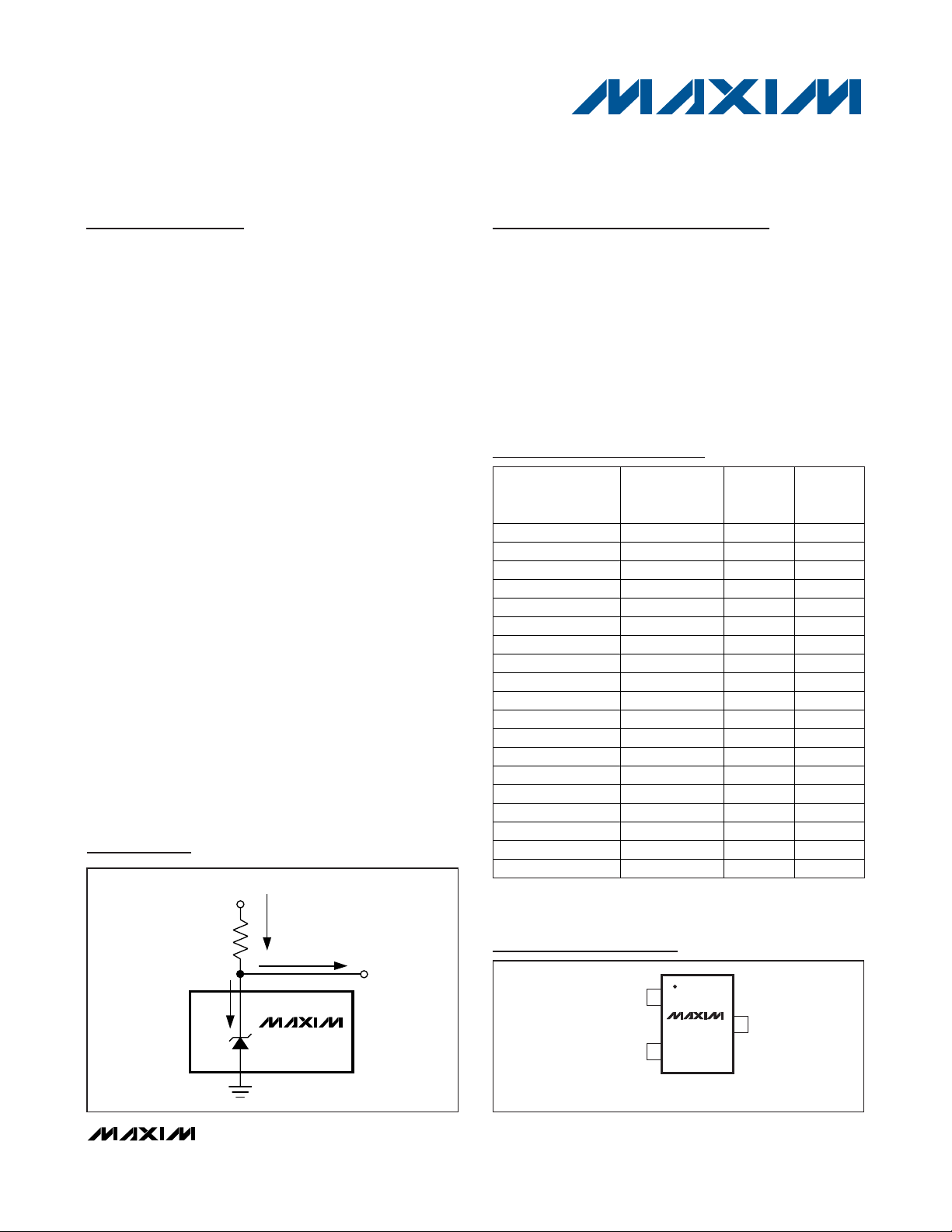
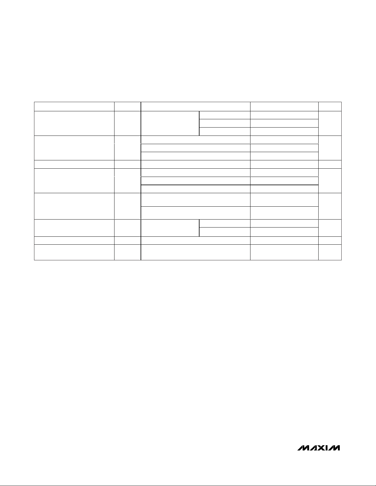
Pin Configuration
Typical Operating Circuit
Selector Guide
19-2563; Rev 6; 9/11
Ordering Information appears at end of data sheet.
+Denotes a lead(Pb)-free/RoHS-compliant package.
T = Tape and reel.
/V
Denotes an automotive qualified parts.
For pricing, delivery, and ordering information, please contact Maxim Direct at 1-888-629-4642,
or visit Maxim’s website at www.maxim-ic.com.
V
S
I
+ I
SHUNT
LOAD
R
S
I
LOAD
V
R
I
SHUNT
LM4050
PIN TEMP RANGE
LM 4050_E M3- 2.1+T
LM 4050_E X 3-2.1+T
LM 4050_E M3- 2.5+T
LM 4050_E X 3-2.5+T
LM 4050_E X 3-2.5/V + T
LM 4050_E M3- 3.0+T
LM 4050_E M3- 3.0/V+ T
LM 4050_E X 3-3.0+T
LM 4050_E M3- 3.3+T
LM 4050_E X 3-3.3+T
LM4050_EX3-3.3/V+T
LM 4050_E M3- 4.1+ T
LM 4050_E M3- 4.1/V+ T
LM 4050_E X 3-4.1+T
LM 4050_E M3- 5.0+ T
LM4050_EM3-5.0/V+T
LM 4050_E X 3-5.0+T
LM 4051_E M3- 1.2+ T
LM 4051_E X 3-1.2+T
- 40°C to + 125°C
- 40°C to + 125°C
- 40°C to + 125°C
- 40°C to + 125°C
- 40°C to + 125°C
- 40°C to + 125°C
- 40°C to + 125°C
- 40°C to + 125°C
- 40°C to + 125°C
- 40°C to + 125°C
- 40°C to + 125°C
- 40°C to + 125°C
- 40°C to + 125°C
- 40°C to + 125°C
- 40°C to + 125°C
- 40°C to + 125°C
- 40°C to + 125°C
- 40°C to + 125°C
- 40°C to + 125°C
PIN-
PACKAGE
3 SOT23 2.048
3 SC70 2.048
3 SOT23 2.500
3 SC70 2.500
3 SC70 2.500
3 SOT23 3.000
3 SOT23 3.000
3 SC70 3.000
3 SOT23 3.300
3 SC70 3.300
3 SC70 3.300
3 SOT23 4.096
3 SOT23 4.096
3 SC70 4.096
3 SOT23 5.000
3 SOT23 5.000
3 SC70 5.000
3 SOT23 1.225
3 SC70 1.225
OUTPUT
VOLTAGE
(V)
TOP VIEW
1
+
LM4050/
LM4051
-
2
3 N.C.*
*PIN 3 MUST BE LEFT UNCONNECTED OR CONNECTED TO PIN 2.
SC70/SOT23
Page 2
LM4050/LM4051
50ppm/°C Precision Micropower Shunt Voltage
References with Multiple Reverse Breakdown Voltages
2 _______________________________________________________________________________________
ABSOLUTE MAXIMUM RATINGS
ELECTRICAL CHARACTERISTICS—1.225V
(IR= 100µA, TA= T
MIN
to T
MAX
, unless otherwise noted. Typical values are at TA= +25°C.) (Note 1)
Stresses beyond those listed under “Absolute Maximum Ratings” may cause permanent damage to the device. These are stress ratings only, and functional
operation of the device at these or any other conditions beyond those indicated in the operational sections of the specifications is not implied. Exposure to
absolute maximum rating conditions for extended periods may affect device reliability.
Reverse Current (cathode to anode) ..................................20mA
Forward Current (anode to cathode) ..................................10mA
Continuous Power Dissipation (T
A
= +70°C)
3-Pin SC70 (derate 2.17mW/°C above +70°C)............174mW
3-Pin SOT23 (derate 4.01mW/°C above +70°C)..........320mW
Operating Temperature Range
LM4050/LM4051_E_ _ _ ................................-40°C to +125°C
Storage Temperature Range .............................-65°C to +150°C
Junction Temperature......................................................+150°C
Lead Temperature (soldering, 10s)..................................+300°C
Soldering Temperature (reflow) .......................................+260°C
Reverse Breakdown Voltage V
Reverse Breakdown Voltage
Tolerance (Note 2)
Minimum Operating Current I
Average Reverse Voltage
Temperature Coefficient
(Notes 2, 3)
Reverse Breakdown Voltage
Change with Operating
Current Change
Reverse Dynamic
Impedance (Note 3)
Wideband Noise e
Reverse Breakdown Voltage
Long-Term Stability
PARAMETER SYMBOL CONDITIONS MIN TYP MAX UNITS
TA = +25°C
R
LM4051A ±1.2 ±7
V
ΔV
RTOL
RMIN
R
Z
ΔV
LM4051B ±2.4 ±9
LM4051C ±6.0 ±12
IR = 10mA ±20
IR = 1mA ±15 ±50
/ΔT
= 100µA ±15
I
R
I
≤ I
RMIN
1mA ≤ I
IR = 1mA, f = 120Hz, IAC = 0.1I
R
IR = 100µA, 10Hz ≤ f ≤ 10kHz 20 µV
N
T = 1000h 120 ppm
R
≤ 1mA 0.7 1.5
R
≤ 12mA 2.5 8.0
R
LM4051A (0.1%) 1.2238 1.2250 1.2262
LM4051B (0.2%) 1.2226 1.2250 1.2275
LM4051C (0.5%) 1.2189 1.2250 1.2311
45 60 µA
R
0.5 1.5 Ω
V
mV
ppm/°C
mV
RMS
Page 3
LM4050/LM4051
50ppm/°C Precision Micropower Shunt Voltage
References with Multiple Reverse Breakdown Voltages
_______________________________________________________________________________________ 3
ELECTRICAL CHARACTERISTICS—2.048V
(IR= 100µA, TA= T
MIN
to T
MAX
, unless otherwise noted. Typical values are at TA= +25°C.) (Note 1)
PARAMETER SYMBOL CONDITIONS MIN TYP MAX UNITS
Reverse Breakdown Voltage V
Reverse Breakdown Voltage
Tolerance (Note 2)
Minimum Operating Current I
Average Reverse Voltage
Temperature Coefficient
(Notes 2, 3)
Reverse Breakdown Voltage
Change with Operating
Current Change
Reverse Dynamic
Impedance (Note 3)
Wideband Noise e
Reverse Breakdown Voltage
Long-Term Stability
TA = +25°C
R
LM4050A ±2.0 ±12
V
ΔV
RTOL
RMIN
R
Z
ΔV
LM4050B ±4.0 ±14
LM4050C ±10 ±20
IR = 10mA ±20
IR = 1mA ±15 ±50
/ΔT
= 100µA ±15
I
R
I
≤ I
RMIN
1mA ≤ I
IR = 1mA, f = 120Hz,
R
I
AC
IR = 100µA, 10Hz ≤ f ≤ 10kHz 28 µV
N
T = 1000h 120 ppm
R
≤ 1mA 0.3 1.0
R
≤ 15mA 2.5 8.0
R
= 0.1I
R LM4050C 0.3 0.9
LM4050A (0.1%) 2.0460 2.0480 2.0500
LM4050B (0.2%) 2.0439 2.0480 2.0521
LM4050C (0.5%) 2.0378 2.0480 2.0582
45 65 µA
LM4050A/B 0.3 0.8
V
mV
ppm/°C
mV
Ω
RMS
Page 4
LM4050/LM4051
50ppm/°C Precision Micropower Shunt Voltage
References with Multiple Reverse Breakdown Voltages
4 _______________________________________________________________________________________
ELECTRICAL CHARACTERISTICS—2.500V
(IR= 100µA, TA= T
MIN
to T
MAX
, unless otherwise noted. Typical values are at TA= +25°C.) (Note 1)
PARAMETER SYMBOL CONDITIONS MIN TYP MAX UNITS
Reverse Breakdown Voltage V
Reverse Breakdown Voltage
Tolerance (Note 2)
Minimum Operating Current I
Average Reverse Voltage
Temperature Coefficient
(Notes 2, 3)
Reverse Breakdown Voltage
Change with Operating
Current Change
Reverse Dynamic
Impedance (Note 3)
Wideband Noise e
Reverse Breakdown Voltage
Long-Term Stability
LM4050A (0.1%) 2.4975 2.5000 2.5025
V
ΔV
R
RTOL
RMIN
/ΔT
R
Z
R
N
ΔV
TA = +25°C
LM4050A ±2.5 ±15
LM4050B ±5.0 ±18
LM4050C ±13 ±25
IR = 10mA ±20
IR = 1mA ±15 ±50
= 100µA ±15
I
R
I
≤ I
RMIN
1mA ≤ I
IR = 1mA, f = 120Hz,
I
AC
IR = 100µA, 10Hz ≤ f ≤ 10kHz 35 µV
T = 1000h 120 ppm
R
≤ 1mA 0.3 1.0
R
≤ 15mA 2.5 8.0
R
= 0.1I
R LM4050C 0.3 0.9
LM4050B (0.2%) 2.4950 2.5000 2.5050
LM4050C (0.5%) 2.4875 2.5000 2.5125
LM4050A/B 0.3 0.8
45 65 µA
V
mV
ppm/°C
mV
Ω
RMS
Page 5
LM4050/LM4051
50ppm/°C Precision Micropower Shunt Voltage
References with Multiple Reverse Breakdown Voltages
_______________________________________________________________________________________ 5
ELECTRICAL CHARACTERISTICS—3.000V
(IR= 100µA, TA= T
MIN
to T
MAX
, unless otherwise noted. Typical values are at TA= +25°C.) (Note 1)
ELECTRICAL CHARACTERISTICS—3.300V
(IR= 100µA, TA= T
MIN
to T
MAX
, unless otherwise noted. Typical values are at TA= +25°C.) (Note 1)
PARAMETER SYMBOL CONDITIONS MIN TYP MAX UNITS
Reverse Breakdown Voltage V
Reverse Breakdown Voltage
Tolerance (Note 2)
Minimum Operating Current I
Average Reverse Voltage
Temperature Coefficient
(Notes 2, 3)
Reverse Breakdown Voltage
Change with Operating
Current Change
Reverse Dynamic
Impedance (Note 3)
Wideband Noise e
Reverse Breakdown Voltage
Long-Term Stability
TA = +25°C
R
LM4050A ±3.0 ±18
V
RTOL
LM4050B ±6.0 ±21
LM4050C ±15 ±30
RMIN
IR = 10mA ±20
IR = 1mA ±15 ±50
/ΔT
ΔV
R
= 100µA ±15
I
R
I
≤ I
≤ 1mA 0.3 1.0
R
≤ 15mA 2.5 8.0
R
= 0.1I
R LM4050C 0.3 0.9
Z
ΔV
RMIN
1mA ≤ I
IR = 1mA, f = 120Hz,
R
I
AC
IR = 100µA, 10Hz ≤ f ≤ 10kHz 45 µV
N
T = 1000h 120 ppm
R
LM4050A (0.1%) 2.9970 3.0000 3.0030
LM4050B (0.2%) 2.9940 3.0000 3.0060
LM4050C (0.5%) 2.9850 3.0000 3.0150
45 67 µA
LM4050A/B 0.3 0.8
V
mV
ppm/°C
mV
Ω
RMS
PARAMETER SYMBOL CONDITIONS MIN TYP MAX UNITS
Reverse Breakdown Voltage V
Reverse Breakdown Voltage
Tolerance (Note 2)
Minimum Operating Current I
Average Reverse Voltage
Temperature Coefficient
(Notes 2, 3)
Reverse Breakdown Voltage
Change with Operating
Current Change
Reverse Dynamic
Impedance (Note 3)
Wideband Noise e
Reverse Breakdown Voltage
Long-Term Stability
TA = +25°C
R
LM4050A ±3.0 ±18
V
RTOL
LM4050B ±6.0 ±21
LM4050C ±15 ±30
RMIN
IR = 10mA ±20
IR = 1mA ±15 ±50
/ΔT
ΔV
R
= 100µA ±15
I
R
I
≤ I
≤ 1mA 0.3 1.0
R
≤ 15mA 2.5 8.0
R
= 0.1I
R LM4050C 0.3 0.9
ΔV
RMIN
1mA ≤ I
Z
IR = 1mA, f = 120Hz,
R
I
AC
IR = 100µA, 10Hz ≤ f ≤ 10kHz 50 µV
N
T = 1000h 120 ppm
R
LM4050A (0.1%) 3.2967 3.3000 3.3033
LM4050B (0.2%) 3.2934 3.3000 3.3066
LM4050C (0.5%) 3.2835 3.3000 3.3165
45 67 µA
LM4050A/B 0.3 0.8
V
mV
ppm/°C
mV
Ω
RMS
Page 6

LM4050/LM4051
50ppm/°C Precision Micropower Shunt Voltage
References with Multiple Reverse Breakdown Voltages
6 _______________________________________________________________________________________
ELECTRICAL CHARACTERISTICS—4.096V
(IR= 100µA, TA= T
MIN
to T
MAX
, unless otherwise noted. Typical values are at TA= +25°C.) (Note 1)
PARAMETER SYMBOL CONDITIONS MIN TYP MAX UNITS
Reverse Breakdown Voltage V
Reverse Breakdown Voltage
Tolerance (Note 2)
Minimum Operating Current I
Average Reverse Voltage
Temperature Coefficient
(Notes 2, 3)
Reverse Breakdown Voltage
Change with Operating
Current Change
Reverse Dynamic
Impedance (Note 3)
Wideband Noise e
Reverse Breakdown Voltage
Long-Term Stability
LM4050A (0.1%) 4.0919 4.0960 4.1001
V
ΔV
R
RTOL
RMIN
/ΔT
R
Z
R
N
ΔV
TA = +25°C
LM4050A ±4.1 ±25
LM4050B ±8.2 ±29
LM4050C ±20 ±41
IR = 10mA ±30
IR = 1mA ±20 ±50
= 100µA ±15
I
R
I
≤ I
RMIN
1mA ≤ I
IR = 1mA, f = 120Hz, IAC = 0.1I
IR = 100µA, 10Hz ≤ f ≤ 10kHz 64 µV
T = 1000h 120 ppm
R
≤ 1mA 0.5 1.2
R
≤ 15mA 3.0 10.0
R
LM4050B (0.2%) 4.0878 4.0960 4.1042
LM4050C (0.5%) 4.0755 4.0960 4.1165
R
50 73 µA
0.5 1.0 Ω
V
mV
ppm/°C
mV
RMS
Page 7

LM4050/LM4051
50ppm/°C Precision Micropower Shunt Voltage
References with Multiple Reverse Breakdown Voltages
_______________________________________________________________________________________ 7
Note 1: All devices are 100% production tested at +25°C and are guaranteed by design for TA= T
MIN
to T
MAX
, as specified.
Note 2: The limit over the full temperature range for the reverse breakdown voltage tolerance is defined as:
[V
RTOL
] ±[(ΔVR/ ΔT) X (maxΔT) X (VR)]
where ΔV
R
/ ΔT is the VRtemperature coefficient, maxΔT is the difference from the +25°C reference point to T
MIN
or T
MAX
,
and V
R
is the reverse breakdown voltage.
The total tolerance over the full temperature range for the different grades where maxΔT = +100°C is shown below:
• A grade: ±0.6% = ±0.1% ±50ppm/°C
100°C
• B grade: ±0.7% = ±0.2% ±50ppm/°C
100°C
• C grade: ±1.0% = ±0.5% ±50ppm/°C
100°C
Note 3: Guaranteed by design.
ELECTRICAL CHARACTERISTICS—5.000V
(IR= 100µA, TA= T
MIN
to T
MAX
, unless otherwise noted. Typical values are at TA= +25°C.) (Note 1)
PARAMETER SYMBOL CONDITIONS MIN TYP MAX UNITS
Reverse Breakdown Voltage V
Reverse Breakdown Voltage
Tolerance (Note 2)
Minimum Operating Current I
Average Reverse Voltage
Temperature Coefficient
(Notes 2, 3)
Reverse Breakdown Voltage
Change with Operating
Current Change
Reverse Dynamic
Impedance (Note 3)
Wideband Noise e
Reverse Breakdown Voltage
Long-Term Stability
TA = +25°C
R
LM4050A ±5.0 ±30
V
RTOL
LM4050B ±10 ±35
LM4050C ±25 ±50
RMIN
IR = 10mA ±30
IR = 1mA ±20 ±50
/ΔT
ΔV
R
I
= 100µA ±15
R
I
≤ I
≤ 1mA 0.5 1.4
R
≤ 15mA 3.5 12.0
R
ΔV
RMIN
1mA ≤ I
Z
IR = 1mA, f = 120Hz, IAC = 0.1I
R
IR = 100µA, 10Hz ≤ f ≤ 10kHz 80 µV
N
T = 1000h 120 ppm
R
LM4050A (0.1%) 4.9950 5.0000 5.0050
LM4050B (0.2%) 4.9900 5.0000 5.0100
LM4050C (0.5%) 4.9750 5.0000 5.0250
54 80 µA
R
0.5 1.1 Ω
V
mV
ppm/°C
mV
RMS
Page 8

LM4050/LM4051
50ppm/°C Precision Micropower Shunt Voltage
References with Multiple Reverse Breakdown Voltages
8 _______________________________________________________________________________________
Typical Operating Characteristics
(IR= 100µA, SC70-3 package, TA= +25°C, unless otherwise noted.)
0
1
2
3
4
5
6
050100
REVERSE CHARACTERISTICS AND
MINIMUM OPERATING CURRENT
LM4050 toc01
REVERSE CURRENT (μA)
REVERSE VOLTAGE (V)
LM4050_I_3-5.0
LM4050_I_3-4.1
LM4050_I_3-3.0
LM4050_I_3-2.5
LM4050_I_3-2.1
LM4050-5.0V
REVERSE VOLTAGE vs. I
SHUNT
LM4050 toc05
I
SHUNT
(mA)
REVERSE VOLTAGE CHANGE (mV)
15105
1
2
3
4
5
6
0
020
TA = -40°C
TA = +125°C
TA = +85°C
TA = +25°C
LM4050-2.5V
REVERSE VOLTAGE vs. I
SHUNT
LM4050 toc04
I
SHUNT
(mA)
REVERSE VOLTAGE CHANGE (mV)
15105
1
2
3
4
5
0
020
TA = +125°C
TA = -40°C
TA = +25°C
TA = +85°C
OUTPUT VOLTAGE vs. TEMPERATURE
= 2.500V)
(V
2.498
2.496
2.494
OUTPUT VOLTAGE (V)
2.492
2.490
-40 135
OUT
TEMPERATURE (°C)
OUTPUT VOLTAGE vs. TEMPERATURE
= 5.000V)
(V
OUT
5.003
5.001
MAX4050 toc02
4.999
4.997
4.995
4.993
OUTPUT VOLTAGE (V)
4.991
4.989
11085603510-15
4.987
-40 135
TEMPERATURE (°C)
MAX4050 toc03
11085-15103560
Page 9

LM4050/LM4051
50ppm/°C Precision Micropower Shunt Voltage
References with Multiple Reverse Breakdown Voltages
_______________________________________________________________________________________ 9
Typical Operating Characteristics (continued)
(IR= 100µA, SC70-3 package, TA= +25°C, unless otherwise noted.)
V
GEN
V
R
AC-COUPLED
+25μA
-25μA
2mV/div
LM4050-2.5V
LOAD-TRANSIENT RESPONSE
LM4050 toc06
10μs/div
CH1: V
GEN
2V/div
CH2: V
R
AC-COUPLED 2mV/div
I
SHUNT
= 100μA ± 25μA, RL = 100kΩ, SEE FIGURE 1.
V
GEN
V
R
AC-COUPLED
+2.5mA
-2.5mA
20mV/div
LM4050-2.5V
LOAD-TRANSIENT RESPONSE
LM4050 toc10
10μs/div
I
SHUNT
= 10mA ± 2.5mA
R
L
= 1kΩ, SEE FIGURE 1.
V
GEN
V
R
AC-COUPLED
+2.5mA
-2.5mA
20mV/div
LM4050-5.0V
LOAD-TRANSIENT RESPONSE
LM4050 toc11
10μs/div
I
SHUNT
= 10mA ± 2.5mA
R
L
= 1kΩ, SEE FIGURE 1.
V
GEN
V
R
AC-COUPLED
+250μA
-250μA
10mV/div
LM4050-5.0V
LOAD-TRANSIENT RESPONSE
LM4050 toc09
10μs/div
I
SHUNT
= 1mA ± 250μA
R
L
= 10kΩ, SEE FIGURE 1.
Figure 1. Load-Transient Test Circuit
LM4050-5.0V
LOAD-TRANSIENT RESPONSE
GEN
V
AC-COUPLED
R
V
40μs/div
I
= 100μA ± 25μA
SHUNT
= 100kΩ, SEE FIGURE 1.
R
L
LM4050 toc07
+25μA
-25μA
10mV/div
LM4050-2.5V
LOAD-TRANSIENT RESPONSE
GEN
V
AC-COUPLED
R
V
10μs/div
I
= 1mA ± 250μA
SHUNT
= 10kΩ, SEE FIGURE 1.
R
L
LM4050 toc08
+250μA
-250μA
10mV/div
I
1kΩ
SHUNT
R
L
V
GEN
+
V
B
-
V
R
Page 10

LM4050/LM4051
50ppm/°C Precision Micropower Shunt Voltage
References with Multiple Reverse Breakdown Voltages
10 ______________________________________________________________________________________
Typical Operating Characteristics (continued)
(IR= 100µA, SC70-3 package, TA= +25°C, unless otherwise noted.)
V
IN
V
OUT
LM4050-2.5V
STARTUP CHARACTERISTICS
LM4050 toc12
01620812424283236
RESPONSE TIME (μs)
5V
0
0
2V
1V
RS = 30kΩ
SEE FIGURE 2.
110010 1k 10k
LM4050-2.5V
NOISE vs. FREQUENCY
LM4050 toc16
FREQUENCY (Hz)
10,000
100
1000
NOISE (nV/√Hz)
110010 1k 10k
LM4050-5.0V
NOISE vs. FREQUENCY
LM4050 toc17
FREQUENCY (Hz)
10,000
100
1000
NOISE (nV/√Hz)
0.1k 10k1k 100k 1M
LM4050-5.0V
OUTPUT IMPEDANCE vs. FREQUENCY
LM4050 toc15
FREQUENCY (Hz)
IMPEDANCE (Ω)
100
0.1
1
10
IR = 150μA
IR = 1mA
C1 = 0
C1 = 1μF
Figure 2. Startup Characteristics Test Circuit
LM4050-5.0V
STARTUP CHARACTERISTICS
5V
IN
V
0
4V
2V
OUT
V
0
RS = 16kΩ
0405020 3010 60 70 80 90
SEE FIGURE 2.
RESPONSE TIME (μs)
LM4050 toc13
OUTPUT IMPEDANCE vs. FREQUENCY
LM4050-2.5V
1000
100
10
IMPEDANCE (Ω)
1
0.1
C1 = 1μF
IR = 150μA
C1 = 0
IR = 1mA
0.1k 10k1k 100k 1M
FREQUENCY (Hz)
LM4050 toc14
R
S
V
1Hz RATE
50%
DUTY CYCLE
IN
V
R
Page 11

LM4050/LM4051
50ppm/°C Precision Micropower Shunt Voltage
References with Multiple Reverse Breakdown Voltages
______________________________________________________________________________________ 11
Detailed Description
The LM4050/LM4051 shunt references use the
bandgap principle to produce a stable, accurate voltage. The device behaves similarly to an ideal zener
diode; a fixed voltage is maintained across its output
terminals when biased with 60µA to 15mA of reverse
current. The LM4050/LM4051 clamps to a voltage of
one diode drop below ground when biased with forward currents up 10mA.
Figure 3 shows a typical operating circuit. The
LM4050/LM4051 are ideal for providing stable references from a high-voltage power supply.
Applications Information
The LM4050/LM4051s’ internal pass transistors are used
to maintain a constant output voltage (V
SHUNT
) by sinking
the necessary amount of current across a source resistor.
The source resistance (RS) is determined from the load
current (I
LOAD
) range, supply voltage (VS) variations,
V
SHUNT
, and desired quiescent current.
Choose the value of RSwhen VSis at a minimum and I
LOAD
is at a maximum. Maintain a minimum I
SHUNT
of 60µA at all
times. The RSvalue should be large enough to keep
I
SHUNT
less than 15mA for proper regulation when VSis
maximum and I
LOAD
is at a minimum. To prevent damage
to the device, I
SHUNT
should never exceed 20mA.
Therefore, the value of RSis bounded by the following
equation:
[V
S(MIN)
- VR] / [60µA + I
LOAD(MAX)
] > RS>
[V
S(MAX)
- VR] / [20mA + I
LOAD(MIN)
]
Choosing a larger resistance minimizes the total power dissipation in the circuit by reducing the shunt current
(P
D(TOTAL)
= V
S
I
SHUNT
). Provide a safety margin to
incorporate the worst-case tolerance of the resistor used.
Ensure that the resistor’s power rating is adequate, using
the following general power equation:
PDR= I
SHUNT
(V
S(MAX)
- V
SHUNT
)
Output Capacitance
The LM4050/LM4051 do not require external capacitors
for frequency stability and are stable for any output
capacitance.
Temperature Performance
The LM4050/LM4051 typically exhibit output voltage
temperature coefficients within ±15ppm/°C. The polarity of the temperature coefficients may be different from
one device to another; some may have positive coefficients, and others may have negative coefficients.
High Temperature Operation
The maximum junction temperature of the LM4050/
LM4051 is +150°C. The maximum operating temperature
for the LM4050/LM4051_E_ is +125°C. At a maximum
load current of 15mA and a maximum output voltage of
5V, the parts dissipate 75mW of power. The power dissipation limits of the 3-pin SC70 call for a derating value of
2.17mW/°C above +70°C and thus for 75mW of power
dissipation, the parts self-heat to 35.56°C above ambient
temperature. If the ambient temperature is +125°C, the
parts operate at 159.56°C, thereby exceeding the maximum junction temperature value of +150°C. For hightemperature operation, care must be taken to ensure the
combination of ambient temperature, output power dissipation, and package thermal resistance does not conspire to raise the device temperature beyond that listed
in the
Absolute Maximum Ratings
. Either reduce the output load current or the ambient temperature to keep the
part within the limits.
Figure 3. Typical Operating Circuit
Pin Description
PIN NAME FUNCTION
1 + Positive Terminal of the Shunt Reference
2 − Negative Terminal of the Shunt Reference
3 N.C. No connection. Leave this pin unconnected or connected to pin 2.
V
S
I
+ I
SHUNT
R
S
I
SHUNT
LOAD
I
LOAD
LM4050
V
R
Page 12

LM4050/LM4051
50ppm/°C Precision Micropower Shunt Voltage
References with Multiple Reverse Breakdown Voltages
12 ______________________________________________________________________________________
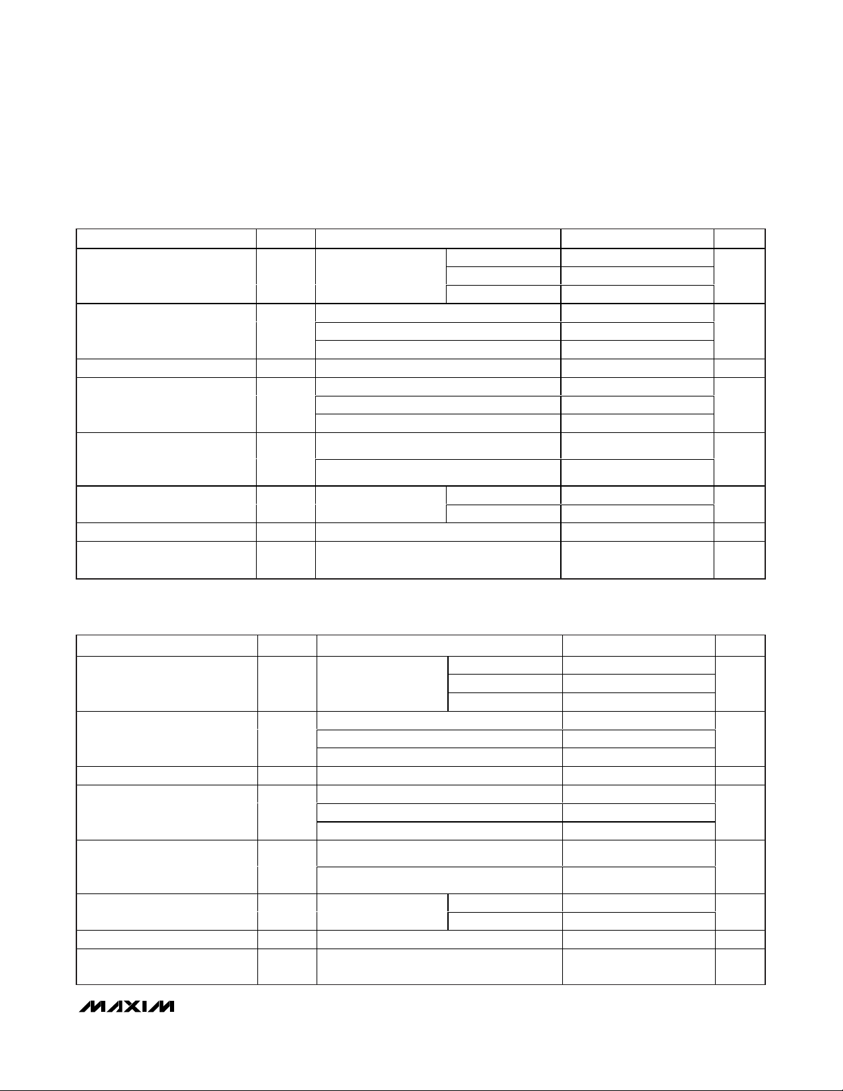
Ordering Information
PART
LM4050AEM3-2.1+T 2.048 0.1 50 -40°C to +125°C 3 SOT23 FZTR
LM4050AEX3-2.1+T 2.048 0.1 50 -40°C to +125°C 3 SC70 ASM
LM4050BEM3-2.1+T 2.048 0.2 50 -40°C to +125°C 3 SOT23 FZTS
LM4050BEX3-2.1+T 2.048 0.2 50 -40°C to +125°C 3 SC70 ASN
LM4050CEM3-2.1+T 2.048 0.5 50 -40°C to +125°C 3 SOT23 FZTT
LM4050CEX3-2.1+T 2.048 0.5 50 -40°C to +125°C 3 SC70 ASO
LM4050AEM3-2.5+T 2.500 0.1 50 -40°C to +125°C 3 SOT23 FZTU
LM4050AEX3-2.5+T 2.500 0.1 50 -40°C to +125°C 3 SC70 ASP
LM4050AEX3-2.5/V+T 2.500 0.1 50 -40°C to +125°C 3 SC70 +AUE
LM4050BEM3-2.5+T 2.500 0.2 50 -40°C to +125°C 3 SOT23 FZTV
LM4050BEX3-2.5+T 2.500 0.2 50 -40°C to +125°C 3 SC70 ASQ
LM4050CEM3-2.5+T 2.500 0.5 50 -40°C to +125°C 3 SOT23 FZTW
LM4050CEX3-2.5+T 2.500 0.5 50 -40°C to +125°C 3 SC70 ASR
LM4050AEM3-3.0+T 3.000 0.1 50 -40°C to +125°C 3 SOT23 FZTX
LM4050AEX3-3.0+T 3.000 0.1 50 -40°C to +125°C 3 SC70 ASS
LM4050BEM3-3.0+T 3.000 0.2 50 -40°C to +125°C 3 SOT23 FZTY
LM4050BEM3-3.0/V+T 3.000 0.2 50 -40°C to +125°C 3 SOT23 +FZVG
LM4050BEX3-3.0+T 3.000 0.2 50 -40°C to +125°C 3 SC70 AST
LM4050CEM3-3.0+T 3.000 0.5 50 -40°C to +125°C 3 SOT23 FZTZ
LM4050CEX3-3.0+T 3.000 0.5 50 -40°C to +125°C 3 SC70 ASU
LM4050AEX3-3.3+T 3.300 0.1 50 -40°C to +125°C 3 SC70 AOJ
LM4050AEX3-3.3/V+T 3.300 0.1 50 -40°C to +125°C 3 SC70 +AUE
LM4050BEX3-3.3+T 3.300 0.2 50 -40°C to +125°C 3 SC70 AOK
LM4050CEX3-3.3+T 3.300 0.5 50 -40°C to +125°C 3 SC70 AOL
LM4050AEM3-4.1+T 4.096 0.1 50 -40°C to +125°C 3 SOT23 FZUA
LM4050AEX3-4.1+T 4.096 0.1 50 -40°C to +125°C 3 SC70 ASV
LM4050BEM3-4.1+T 4.096 0.2 50 -40°C to +125°C 3 SOT23 FZUB
LM4050BEM3-4.1/V+T 4.096 0.2 50 -40°C to +125°C 3 SOT23 +FZVL
LM4050BEX3-4.1+T 4.096 0.2 50 -40°C to +125°C 3 SC70 ASW
LM4050CEM3-4.1+T 4.096 0.5 50 -40°C to +125°C 3 SOT23 FZUC
LM4050CEX3-4.1+T 4.096 0.5 50 -40°C to +125°C 3 SC70 ASX
LM4050AEM3-5.0+T 5.000 0.1 50 -40°C to +125°C 3 SOT23 FZUD
LM4050AEX3-5.0+T 5.000 0.1 50 -40°C to +125°C 3 SC70 ASY
LM4050BEM3-5.0+T 5.000 0.2 50 -40°C to +125°C 3 SOT23 FZUE
LM4050BEX3-5.0+T 5.000 0.2 50 -40°C to +125°C 3 SC70 ASZ
LM4050CEM3-5.0+T 5.000 0.5 50 -40°C to +125°C 3 SOT23 FZUF
LM4050CEM3-5.0/V+T 5.000 0.5 50 -40°C to +125°C 3 SOT23 +FZVM
LM4050CEX3-5.0+T 5.000 0.5 50 -40°C to +125°C 3 SC70 ATA
O U T PU T
VO L T A G E ( V)
I N I T I A L
A C C U R A C Y ( % )
TEMPCO
(ppm/_ C)
TEMP RANGE
PINPACKAGE
TOP
MARK
Page 13

LM4050/LM4051
50ppm/°C Precision Micropower Shunt Voltage
References with Multiple Reverse Breakdown Voltages
______________________________________________________________________________________ 13
Chip Information
PROCESS: BiCMOS
Package Information
For the latest package outline information and land patterns
(footprints), go to www.maxim-ic.com/packages
. Note that a
“+”, “#”, or “-” in the package code indicates RoHS status only.
Package drawings may show a different suffix character, but
the drawing pertains to the package regardless of RoHS status.
PACKAGE
TYPE
PACKAGE
CODE
OUTLINE
NO.
LAND
PATTERN NO.
3 SOT23 U3+1
90-0179
3 SC70 X3+2
90-0208
PART
O U T PU T
I N I T I A L
TEMPCO
TEMP RANGE
PINPACKAGE
TOP
MARK
LM4051AEM3-1.2+T 1.225 0.1 50 -40°C to +125°C 3 SOT23 FZTO
LM4051AEX3-1.2+T 1.225 0.1 50 -40°C to +125°C 3 SC70 ASJ
LM4051BEM3-1.2+T
1.225
0.2 50 -40°C to +125°C 3 SOT23 FZTP
LM4051BEX3-1.2+T
1.225
0.2 50 -40°C to +125°C 3 SC70 ASK
LM4051CEM3-1.2+T
1.225
0.5 50 -40°C to +125°C 3 SOT23 FZTQ
LM4051CEX3-1.2+T
1.225
0.5 50 -40°C to +125°C 3 SC70 ASL
Ordering Information (continous)
VO L T A G E ( V)
A C C U R A C Y ( % )
(ppm/_ C)
21-0051
21-0075
Page 14

LM4050/LM4051
50ppm/°C Precision Micropower Shunt Voltage
References with Multiple Reverse Breakdown Voltages
Maxim cannot assume responsibility for use of any circuitry other than circuitry entirely embodied in a Maxim product. No circuit patent licenses are
implied. Maxim reserves the right to change the circuitry and specifications without notice at any time.
14
____________________Maxim Integrated Products, 120 San Gabriel Drive, Sunnyvale, CA 94086 408-737-7600
© 2011 Maxim Integrated Products Maxim is a registered trademark of Maxim Integrated Products, Inc.
Revision History
REVISION
NUMBER
REVISION
DATE
DESCRIPTION PAGES CHANGED
0 7/02 Initial release —
4 5/09
Added lead-free notation and corrected topmarks in the
Ordering Information and Selector Guide sections
1, 12
5 5/11
Added automotive packages and updated the Absolute
Maximum Ratings.
1, 2
6 9/11
Added automotive packages to Selector Guide and
Ordering Information.
1, 12
 Loading...