

For pricing, delivery, and ordering information, please contact Maxim/Dallas Direct! at
1-888-629-4642, or visit Maxim’s website at www.maxim-ic.com.
General Description
The LM4041 is a precision two-terminal shunt mode,
bandgap voltage reference with a fixed reverse breakdown voltage of 1.225V. Ideal for space-critical applications, the LM4041 is offered in the subminiature 3-pin
SC70 surface-mount package (1.8mm
✕
1.8mm), 50%
smaller than comparable devices in SOT23 surfacemount packages (SOT23 versions are also available).
Laser-trimmed resistors ensure precise initial accuracy.
With a 100ppm/°C temperature coefficient, the device
is offered in four grades of initial accuracy ranging from
0.1% to 1%. The LM4041 has a 60µA to 12mA shunt
current capability with low dynamic impedance, ensuring stable reverse-breakdown voltage accuracy over a
wide range of operating temperatures and currents.
The LM4041 does not require an external stabilizing
capacitor while ensuring stability with any capacitive
load.
The LM4041 is guaranteed over the temperature range
-40°C to +125°C.
________________________Applications
Portable, Battery-Powered Equipment
Notebook Computers
Cell Phones
Industrial Process Controls
Features
♦ Ultra-Small 3-Pin SC70 Package
♦ 0.1% (max) Initial Accuracy
♦ 100ppm/°C (max) Temperature Coefficient
Guaranteed over -40°C to +125°C Temperature
Range
♦ Wide Operating Current Range: 60µA to 12mA
♦ Low 20µV
RMS
Output Noise (10Hz to 10kHz)
♦ 1.225V Fixed Reverse Breakdown Voltage
♦ No Output Capacitors Required
♦ Tolerates Capacitive Loads
LM4041
Improved Precision Micropower
Shunt Voltage Reference
________________________________________________________________ Maxim Integrated Products 1
-
1
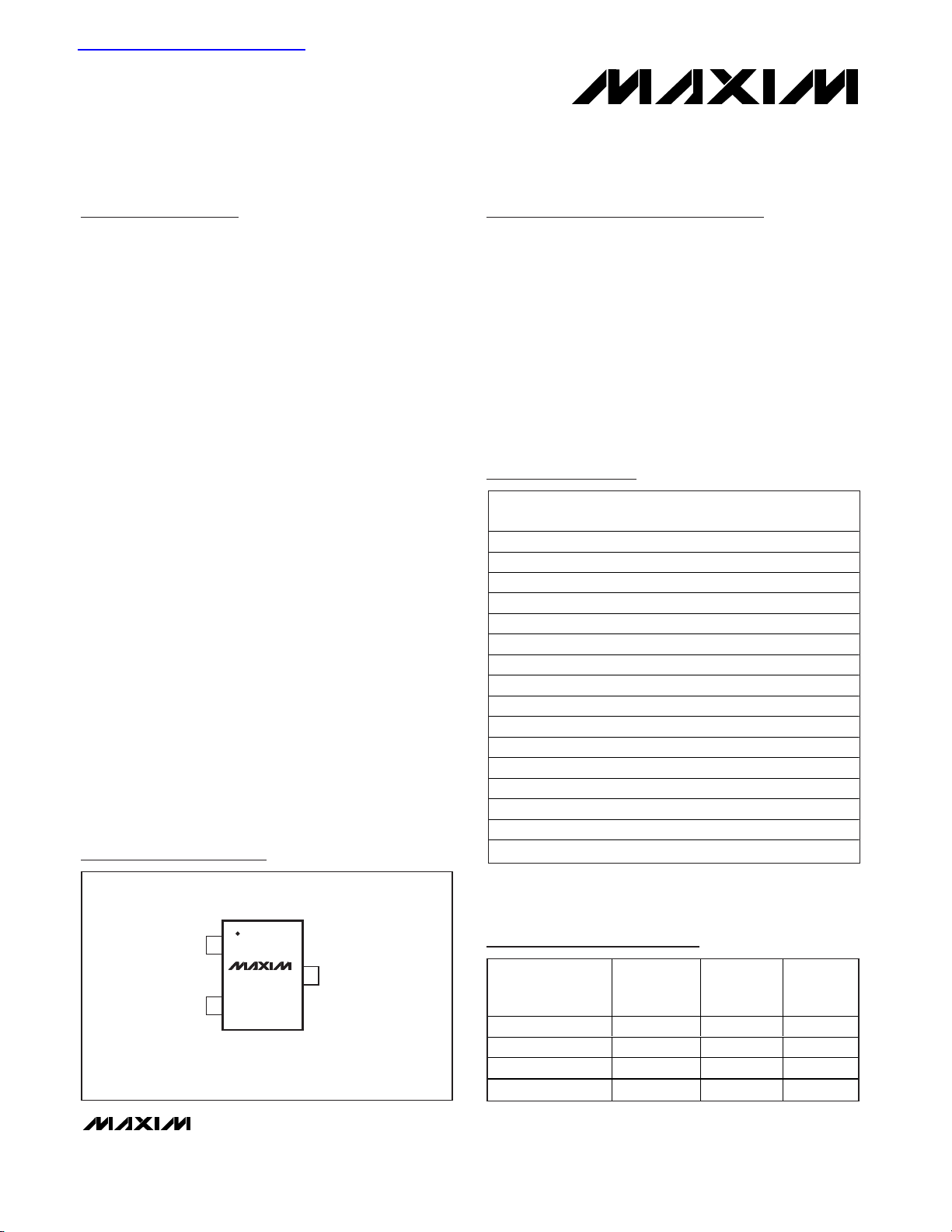
3 N.C.*
+
LM4041
SC70-3/SOT23-3
TOP VIEW
2
*PIN 3 MUST BE LEFT FLOATING OR CONNECTED TO PIN 2.
Pin Configuration
Selector Guide
19-1704; Rev 4; 7/05
Ordering Information
PART
TEMP RANGE
PIN-
TOP
MARK
LM4041AIX3-1.2-T
-40°C to +85°C 3 SC70-3
ABF
LM4041AIM3-1.2-T
-40°C to +85°C
FZEB
LM4041AEX3-1.2-T
3 SC70-3
ALB
LM4041AEM3-1.2-T
FZNC
LM4041BIX3-1.2-T
-40°C to +85°C 3 SC70-3
ABG
LM4041BIM3-1.2-T
-40°C to +85°C
FZEC
LM4041BEX3-1.2-T
3 SC70-3
ALC
LM4041BEM3-1.2-T
FZND
LM4041CIX3-1.2-T
-40°C to +85°C 3 SC70-3
ABH
LM4041CIM3-1.2-T
-40°C to +85°C
FZED
LM4041CEX3-1.2-T
3 SC70-3
ALD
LM4041CEM3-1.2-T
FZNE
LM4041DIX3-1.2-T
-40°C to +85°C 3 SC70-3
ABI
LM4041DIM3-1.2-T
-40°C to +85°C
FZEE
LM4041DEX3-1.2-T
3 SC70-3
ALE
LM4041DEM3-1.2-T
FZNF
*See Selector Guide for a listing of LM4041 Output Voltage,
Initial Accuracy, and Temperature Coefficient specifications.
查询LM4040_EM3-2.5供应商
PACKAGE
3 SOT23-3
-40°C to +125°C
-40°C to +125°C 3 SOT23-3
3 SOT23-3
-40°C to +125°C
-40°C to +125°C 3 SOT23-3
3 SOT23-3
-40°C to +125°C
-40°C to +125°C 3 SOT23-3
3 SOT23-3
-40°C to +125°C
-40°C to +125°C 3 SOT23-3
INITIAL
PART
LM4041A___-1.2-T 0.1 1.225 100
LM4041B___-1.2-T 0.2 1.225 100
LM4041C___-1.2-T 0.5 1.225 100
LM4041D___-1.2-T 1.0 1.225 150
ACCURACY
(%)
OUTPUT
VOLTAGE
(V)
TEMPCO
(ppm/°C)
LM4041
Improved Precision Micropower
Shunt Voltage Reference
2 _______________________________________________________________________________________
ABSOLUTE MAXIMUM RATINGS
ELECTRICAL CHARACTERISTICS
(IR= 100µA, TA= T
MIN
to T
MAX
, unless otherwise noted. Typical values are at TA= +25°C.) (Note 1)
Stresses beyond those listed under “Absolute Maximum Ratings” may cause permanent damage to the device. These are stress ratings only, and functional
operation of the device at these or any other conditions beyond those indicated in the operational sections of the specifications is not implied. Exposure to
absolute maximum rating conditions for extended periods may affect device reliability.
Reverse Current (cathode to anode) ..................................20mA
Forward Current (anode to cathode) ..................................10mA
Continuous Power Dissipation (T
A
= +70°C)
3-Pin SC70 (derate 2.17mW/°C above +70°C)............174mW
3-Pin SOT23 (derate 4.01mW/°C above +70°C)..........320mW
Operating Temperature Range
LM4041_I_ _ _..................................................-40°C to +85°C
LM4041_E_ _ _ ..............................................-40°C to +125°C
Storage Temperature Range .............................-65°C to +150°C
Junction Temperature......................................................+150°C
Lead Temperature (soldering, 10s) ................................+300° C
PARAMETER
SYMBOL
CONDITIONS
MIN
TYP
MAX
UNITS
LM4041A (0.1%)
LM4041B (0.2%)
LM4041C (0.5%)
Reverse Breakdown Voltage V
R
TA = +25°C
LM4041D (1.0%)
V
LM4041A (0.1%)
LM4041B (0.2%)
LM4041C (0.5%)
±14
Reverse Breakdown Voltage
Tolerance (Note 2)
∆V
R
LM4041D (1.0%) ±12 ±24
mV
LM4041A/B/C 45 60
Minimum Operating Current
LM4041D 45 65
µA
IR = 10mA ±20
LM4041A/B/C ±15
IR = 1mA
LM4041D ±15
Average Reverse Voltage
Temperature Coefficient
(Notes 2 and 3)
IR = 100µA ±15
ppm/°C
LM4041A/B/C 0.7 1.5
I
RMIN
≤ I
R
≤ 1mA
LM4041D 0.7 2.0
LM4041A/B/C 2.5 8.0
Reverse Breakdown Voltage
Change with Operating
Current Change
1mA ≤ I
R
≤ 12mA
LM4041D 2.5
mV
LM4041A/B/C 0.5 1.5
Reverse Dynamic
Impedance (Note 3)
Z
R
IR = 1mA, f = 120Hz,
I
AC
= 0.1I
R LM4041D 0.5 2.0
Ω
1.2238 1.2250 1.2262
1.2226 1.2250 1.2275
1.2189 1.2250 1.2311
1.2128 1.2250 1.2373
±1.2 ±9.2
±2.4 ±10.4
±6.0
I
RMIN
∆VR/∆T
∆VR/∆I
R
±100
±150
10.0
LM4041
Improved Precision Micropower
Shunt Voltage Reference
_______________________________________________________________________________________ 3
ELECTRICAL CHARACTERISTICS (continued)
(IR= 100µA, TA= T
MIN
to T
MAX
, unless otherwise noted. Typical values are at TA= +25°C.) (Note 1)
Note 1: All devices are 100% production tested at +25°C and are guaranteed by design for T
A
= T
MIN
to T
MAX
, as specified.
Note 2: The overtemperature limit for Reverse Breakdown Voltage Tolerance is defined as the room-temperature Reverse
Breakdown Voltage Tolerance ±[(
∆VR/ ∆T)(max∆T)(VR)], where ∆VR/ ∆T is the VRtemperature coefficient, max∆T is the
maximum difference in temperature from the reference point of +25°C to T
MIN
or T
MAX
, and VRis the reverse breakdown
voltage. The total overtemperature tolerance for the different grades in the temperature range where max∆T = +65°C is
shown below:
A grade: ±0.75% = ±0.1% ±100ppm/°C
✕
65°C
B grade: ±0.85% = ±0.2% ±100ppm/°C
✕
65°C
C grade: ±1.15% = ±0.5% ±100ppm/°C
✕
65°C
D grade: ±1.98% = ±1.0% ±150ppm/°C
✕
65°C
The total overtemperature tolerance for the different grades in the extended temperature range where max∆T = +100°C is
shown below:
A grade: ±1.1% = ±0.1% ±100ppm/°C
✕
100°C
B grade: ±1.2% = ±0.2% ±100ppm/°C
✕
100°C
C grade: ±1.5% = ±0.5% ±100ppm/°C
✕
100°C
D grade: ±2.5% = ±1.0% ±150ppm/°C
✕
100°C
Therefore, as an example, the A-grade LM4041-1.2 has an overtemperature reverse breakdown voltage tolerance of ±2.5V
x 0.75% = ±19mV.
Note 3: Guaranteed by design.
PARAMETER
SYMBOL
CONDITIONS
MIN
TYP
MAX
UNITS
Wideband Noise e
N
IR = 100µA, 10Hz ≤ f ≤ 10kHz 20
µV
RMS
Reverse Breakdown Voltage
Long-Term Stability
∆V
R
T = 1000h, IR = 100µA 120
ppm
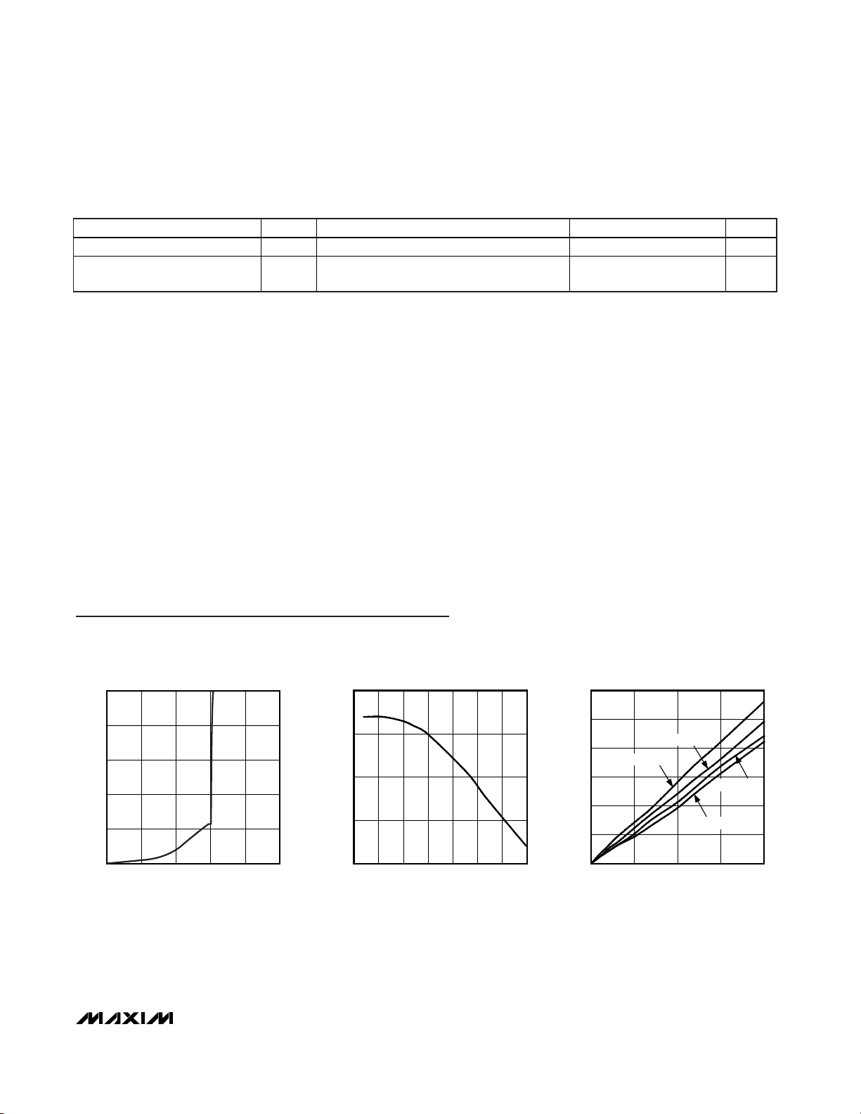
TEMPERATURE DRIFT
LM4041 toc02
TEMPERATURE (°C)
REFERENCE VOLTAGE CHANGE (mV)
1007550250-25
-2
-1
0
1
-3
-50 125
REVERSE VOLTAGE vs. CURRENT
LM4041 toc03
SOURCE CURRENT (mA)
REVERSE VOLTAGE CHANGE (mV)
15105
1
2
3
4
5
6
0
020
TA = +25°C
TA = -40°C
TA = +125°C
TA = +85°C
Typical Operating Characteristics
(IR= 100µA, SC70-3 package, TA= +25°C, unless otherwise noted.)
0
20
60
40
80
100
0 0.80.4 1.2 1.6 2.0
REVERSE CHARACTERISTICS AND
MINIMUM OPERATING CURRENT
LM4041-01
REVERSE VOLTAGE (V)
REVERSE CURRENT (µA)
LM4041
Improved Precision Micropower
Shunt Voltage Reference
4 _______________________________________________________________________________________
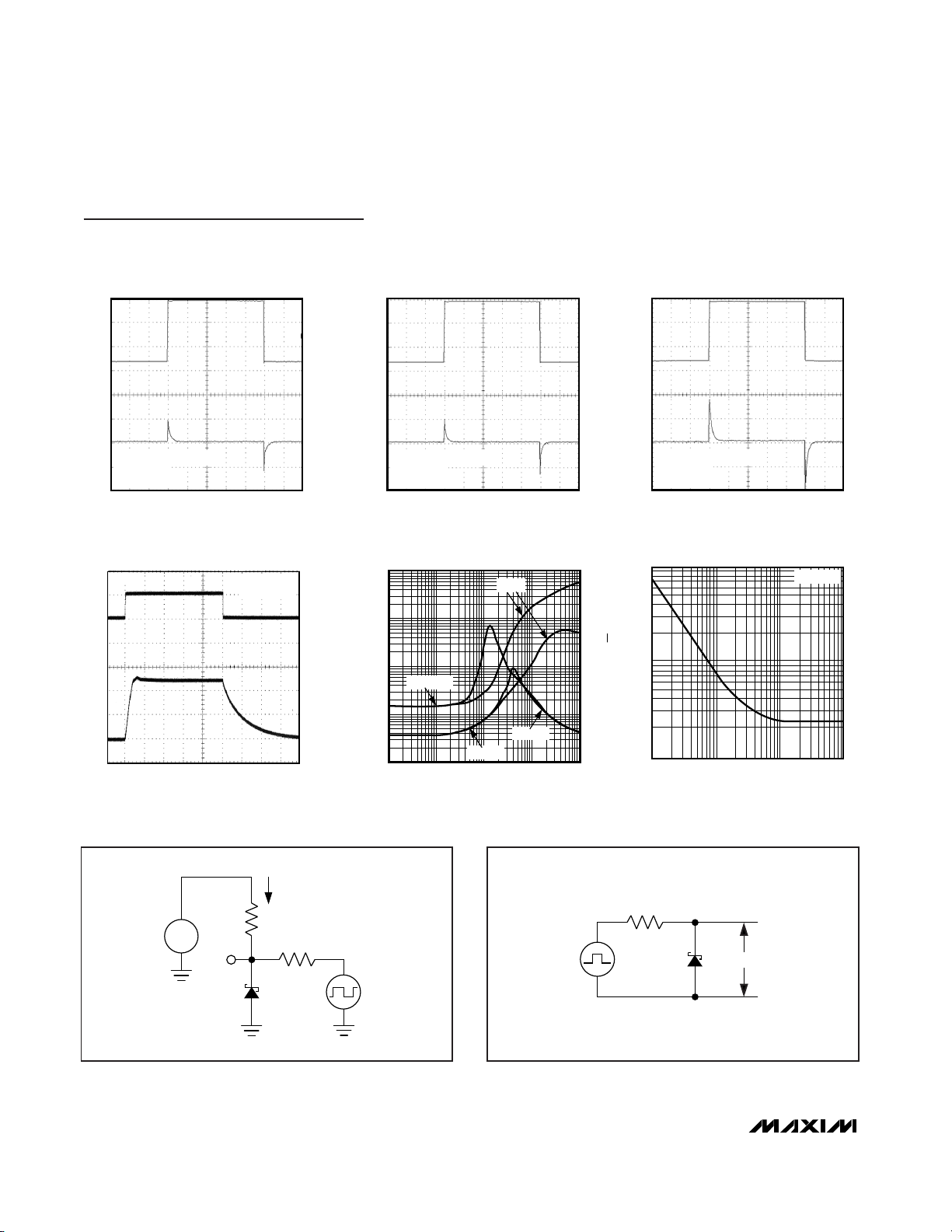
100 10k1k 100k 1M
OUTPUT IMPEDANCE vs. FREQUENCY
LM4041-08
FREQUENCY (Hz)
IMPEDANCE (Ω)
1000
0.1
1
10
100
C1 = 0
IR =
C1 = 1µF
IR = 1mA
150µA
10,000
100
10 1k 10k
1000
FREQUENCY (Hz)
100
NOISE vs. FREQUENCY
LM4041-09
IR = 200µA
NOISE (nV/√Hz)
RS = 30k
Ω
SEE FIGURE 2
0841216
STARTUP CHARACTERISTICS
LM4041-07
RESPONSE TIME (µs)
5V
V
IN
OV
0V
1.5V
1.0V
V
OUT
O.5V
V
GEN
V
R
(AC-COUPLED)
2V/div
2mV/div
LOAD-TRANSIENT RESPONSE
LM4041-05
10µs/div
I
SHUNT
= 1mA ± 250µA,
R
L
= 10k
Ω
SEE FIGURE 1
V
GEN
V
R
2V/div
2mV/div
LOAD-TRANSIENT RESPONSE
LM4041-06
10µs/div
I
SHUNT
= 10mA ± 2.5mA,
R
L
= 1k
Ω
SEE FIGURE 1
V
GEN
V
R
(AC-COUPLED)
2V/div
2mV/div
LOAD-TRANSIENT RESPONSE
LM4041-04
10µs/div
I
SHUNT
= 100µA ± 25µA,
R
L
= 100k
Ω
SEE FIGURE 1
Typical Operating Characteristics (continued)
(IR= 100µA, SC70-3 package, TA= +25°C, unless otherwise noted.)
R
S
30kΩ
V
IN
1Hz RATE
V
R
Figure 2. Startup Characteristics Test Circuit
1kΩ
V
B
+
-
I
SHUNT
V
R
R
L
V
GEN
Figure 1. Load-Transient Test Circuit
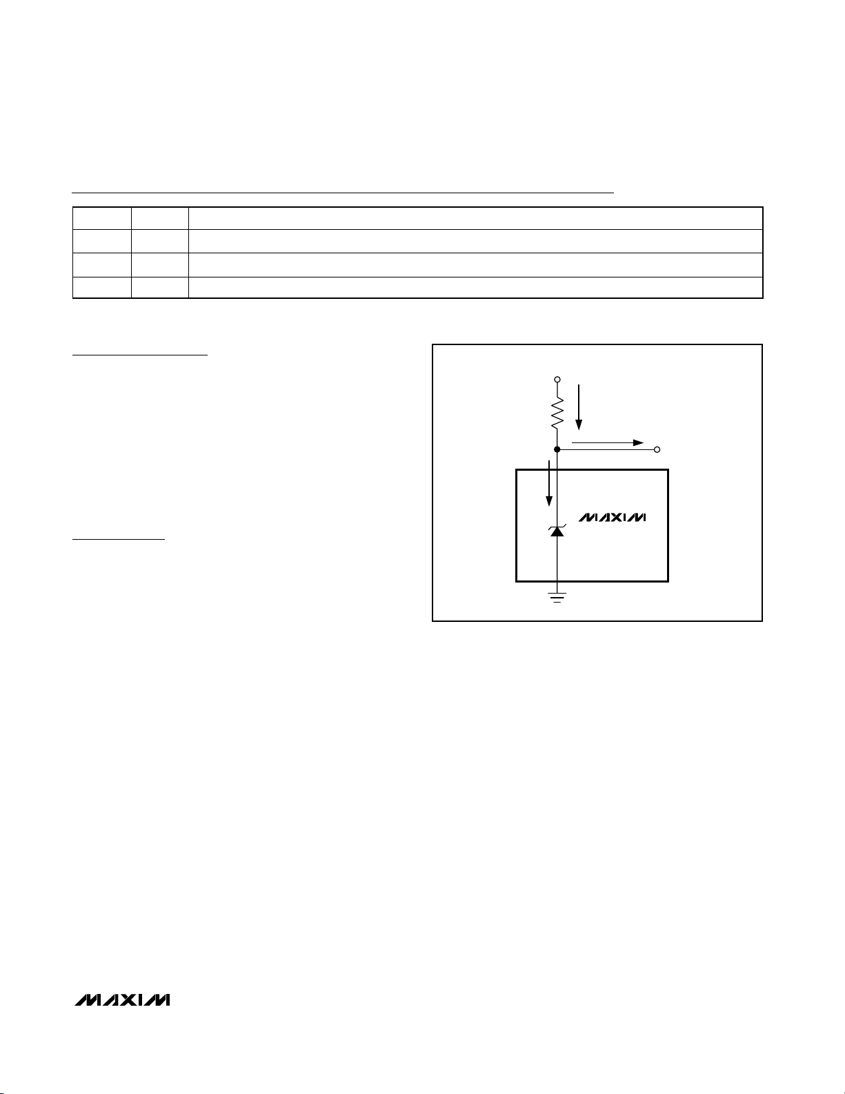
Detailed Description
The LM4041 shunt references use the bandgap principle to produce a stable, accurate voltage. The device
behaves similarly to an ideal zener diode; a fixed voltage of +1.225V is maintained across its output terminals when biased with 60µA to 12mA of reverse
current. The LM4041 behaves similarly to a silicon
diode when biased with forward currents up 10mA.
Figure 3 shows a typical operating circuit. The LM4041
is ideal for providing a stable reference from a highvoltage power supply.
Applications Information
The LM4041’s internal pass transistor is used to maintain a constant output voltage (V
SHUNT
) by sinking the
necessary amount of current across a source resistor.
The source resistance (RS) is determined from the load
current (I
LOAD
) range, supply voltage (VS) variations,
V
SHUNT
, and desired quiescent current.
Choose the value of RSwhen VSis at a minimum and
I
LOAD
is at a maximum. Maintain a minimum I
SHUNT
of
60µA at all times. The RSvalue should be large enough
to keep I
SHUNT
less than 12mA for proper regulation
when V
S
is maximum and I
LOAD
is at a minimum. To
prevent damage to the device, I
SHUNT
should never
exceed 20mA.
Therefore, the value of R
S
is bounded by the following
equation:
[V
S(MIN)
- VR] / [60µA + I
LOAD(MAX)
] > RS>
[V
S(MAX)
- VR] / [20mA + I
LOAD(MIN)
]
Choosing a larger resistance minimizes the total power
dissipation in the circuit by reducing the shunt current
(P
D(TOTAL)
= V
S
✕
I
SHUNT
). Provide a safety margin to
incorporate the worst-case tolerance of the resistor
used. Ensure that the resistor’s power rating is adequate, using the following general power equation:
PR= I
SHUNT
✕
(V
S(MAX)
- VR)
Output Capacitance
The LM4041 does not require an external capacitor for
frequency stability and is stable for any output capacitance.
Temperature Performance
The LM4041 typically exhibits an output voltage temperature coefficient within ±15ppm/°C. The polarity of
the temperature coefficient may be different from one
device to another; some may have positive coefficients,
and others may have negative coefficients.
LM4041
Improved Precision Micropower
Shunt Voltage Reference
_______________________________________________________________________________________ 5
Pin Description
PIN
NAME
FUNCTION
1+Positive Terminal of the Shunt Reference
2 − Negative Terminal of the Shunt Reference
3 N.C. Leave this pin unconnected, or connect to pin 2.
Figure 3. Typical Operating Circuit
LM4041
I
LOAD
I
SHUNT
R
S
V
S
V
R
I
SHUNT
+ I
LOAD

LM4041
High Temperature Operation
The maximum junction temperature of the LM4041 is
+150°C. The maximum operating temperature for the
LM4041_E_ is +125°C. At a maximum load current of
15mA and a maximum output voltage of 5V, the part
will dissipate 75mW of power. The power dissipation
limits of the 3-pin SC70 call for a derating value of
2.17mW/°C above +70°C and thus for 75mW of power
dissipation, the part will selfheat to 35.56°C above
ambient temperature. If the ambient temperature is
+125°C, the part operates at 159.56°C, thereby
exceeding the maximum junction temperature value of
+150°C. For high-temperature operation, care must be
taken to ensure the combination of ambient temperature, output power dissipation, and package thermal
resistance does not conspire to raise the device temperature beyond that listed in the Absolute Maximum
Ratings. Either reduce the output load current or the
ambient temperature to keep the part within the limits.
Improved Precision Micropower
Shunt Voltage Reference
6 _______________________________________________________________________________________
Chip Information
TRANSISTOR COUNT: 60
PROCESS: BiCMOS
LM4041
Improved Precision Micropower
Shunt Voltage Reference
_______________________________________________________________________________________ 7
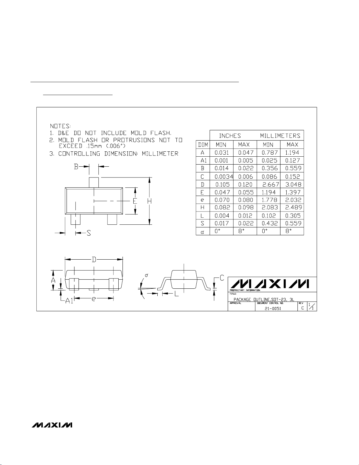
SOTPO3L.EPS
Package Information
(The package drawing(s) in this data sheet may not reflect the most current specifications. For the latest package outline information
go to www.maxim-ic.com/packages
.)
LM4041
Improved Precision Micropower
Shunt Voltage Reference
Maxim cannot assume responsibility for use of any circuitry other than circuitry entirely embodied in a Maxim product. No circuit patent licenses are
implied. Maxim reserves the right to change the circuitry and specifications without notice at any time.
8 _____________________Maxim Integrated Products, 120 San Gabriel Drive, Sunnyvale, CA 94086 408-737-7600
© 2005 Maxim Integrated Products Printed USA is a registered trademark of Maxim Integrated Products, Inc.
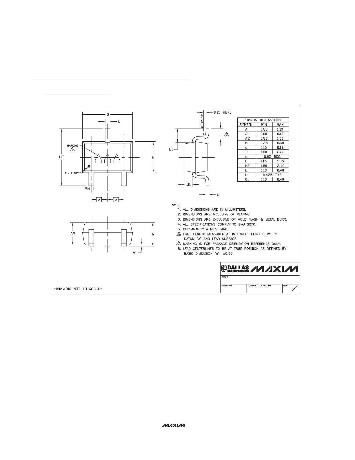
SC70, 3L.EPS
PACKAGE OUTLINE, 3L SC70
21-0075
1
1
C
Package Information (continued)
(The package drawing(s) in this data sheet may not reflect the most current specifications. For the latest package outline information
go to www.maxim-ic.com/packages
.)
 Loading...