

General Description
The ICL761X–ICL764X family of monolithic CMOS op
amps combine ultra-low input current with low-power
operation over a wide supply voltage range. With pinselectable quiescent currents of 10µA, 100µA, or
1000µA per amplifier, these op amps will operate from
±1V to ±8V power supplies, or from single supplies
from 2V to 16V. The CMOS outputs swing to within millivolts of the supply voltages.
The ultra-low bias current of 1pA makes this family of
op amps ideal for long time constant integrators,
picoammeters, low droop rate sample/hold amplifiers
and other applications where input bias and offset currents are critical. A low noise current of 0.01pA√Hz and
an input impedance of 1012Ω ensure optimum performance with very high source impedances in such
applications as pH meters and photodiode amplifiers.
Applications
Battery-Powered Instruments
Low-Leakage Amplifiers
Long-Time Constant Integrators
Low-Frequency Active Filters
Hearing Aids and Microphone Amplifiers
Low Droop Rate Sample/Hold Amplifiers
Picoammeters
Features
o Pin-for-Pin Second Source
o 1pA Typical Bias Current—4nA (max) at +125°C
o ±1V to ±8V Wide Supply Voltage Range
o Industry-Standard Pinouts
o Programmable Quiescent Currents of 10µA,
100µA, and 1000µA
o Monolithic, Low-Power CMOS Design
ICL761X–ICL764X
Single/Dual/Triple/Quad
Operational Amplifiers
________________________________________________________________
Maxim Integrated Products
1
Ordering Information
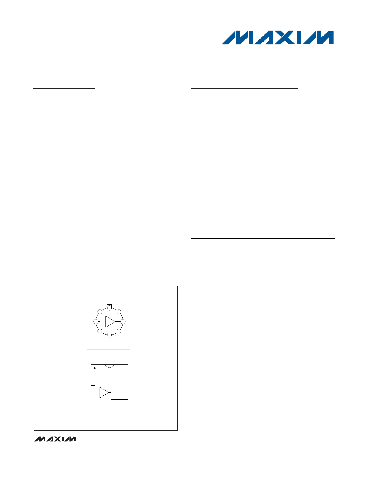
Pin Configuration
19-0942; Rev 3; 5/10
Typical Operating Circuit appears at end of data sheet.
For pricing, delivery, and ordering information, please contact Maxim Direct at 1-888-629-4642,
or visit Maxim’s website at www.maxim-ic.com.
TOP VIEW SINGLES—ICL7611/12/14/16
OFFSET
IN
+IN
TO—99
SET)*
(I
O
OFFSET
-IN
1
2
3
8
1
3
+IN
4
V-
*PIN 7 CONNECTED TO CASE
8-PIN DIP
7
5
V+
62
OFFSET
OUTPUT
8
7
6
(I
V+
OUT
O
SET)*
ICL76XX M N OP
V
OS
SELECTION
A = 2mV
B = 5mV
C = 10mV
D = 15mV
E = 20mV
TEMP
RANGE
C = 0°C to
70°C
E = -40°C to
+85°C
M = -55°C to
+125°C
PKG CODE
TV= 8-Pin TO99
PA = 8-Pin
Plastic Dip
SA = 8-Pin
Small SO
JD = 14-Pin
CERDIP
PD = 14-Pin
Plastic Dip
SD = 14-Pin
Small SO
JE = 16-Pin
CERDIP
PE = 16-Pin
Plastic Dip
SE = 16-Pin
Small SO
WE – 16-Pin
Wide SO
4
V-
*EXTERNAL COMPENSATION (ICL7614)
5
OFFSET
ICL761X–ICL764X
Single/Dual/Triple/Quad
Operational Amplifiers
2 _______________________________________________________________________________________
Ordering Information (Single/Dual)
Note: X above is replaced by: 1, 2, 4, 8.
Ordering Information (continued)
ICL7611
ICL7612
ICL7614
ICL7616
ICL7621
ICL7622
ICL7631
ICL7632
Compensated X X X X X X X X
Externally
Compensated
Extended
CMVR
Offset null
capability
Programmable
I
Q
Fixed IQ-10µA X
Fixed IQ100µA
Fixed IQ-1mA X
XXXX X
XX X XX
X
XX
XXX
ICL7641
ICL7642
PART TEMP RANGE PIN-PACKAGE
ICL761XACPA 0°C to +70°C 8 Plastic Dip
ICL761XACSA 0°C to +70°C 8 Slim SO
ICL761XACTV 0°C to +70°C TO-99 Metal Can
ICL761XAMTV -55°C to +125°C TO-99 Metal Can
ICL761XBCPA 0°C to +70°C 8 Plastic Dip
ICL761XBCSA 0°C to +70°C 8 Slim SO
ICL761XBCTV 0°C to +70°C TO-99 Metal Can
ICL761XBESA -40°C to +85°C 8 Slim SO
ICL761XBMTV -55°C to +125°C TO-99 Metal Can
ICL761XDCPA 0°C to +70°C 8 Plastic Dip
ICL761XDCSA 0°C to +70°C 8 Slim SO
ICL761XDCTV 0°C to +70°C TO-99 Metal Can
ICL761XDESA -40°C to +85°C 8 Slim SO
ICL7621ACPA 0°C to +70°C 8 Plastic Dip
ICL7621ACSA 0°C to +70°C 8 Slim SO
ICL7621ACTV 0°C to +70°C TO-99 Metal Can
ICL7621AMTV -55°C to +125°C TO-99 Metal Can
ICL7621BCPA 0°C to +70°C 8 Plastic Dip
PART TEMP RANGE PIN-PACKAGE
ICL7621BCSA 0°C to +70°C 8 Slim SO
ICL7621BCTV 0°C to +70°C TO-99 Metal Can
ICL7621BMTV -55°C to +125°C TO-99 Metal Can
ICL7621DCPA 0°C to +70°C 8 Plastic Dip
ICL7621DCSA 0°C to +70°C 8 Slim SO
ICL7621DCTV 0°C to +70°C TO-99 Metal Can
ICL7622ACPD 0°C to +70°C 14 Plastic Dip
ICL7622ACSD 0°C to +70°C 14 Slim SO
ICL7622ACJD 0°C to +70°C 14 CERDIP
ICL7622AMJD -55°C to +125°C 14 CERDIP
ICL7622BCPD 0°C to +70°C 14 Plastic Dip
ICL7622BCSA 0°C to +70°C 14 Slim SO
ICL7622BCJD 0°C to +70°C 14 CERDIP
ICL7622BMJD -55°C to +125°C 14 CERDIP
ICL7622DCPD 0°C to +70°C 14 Plastic Dip
ICL7622DCSD 0°C to +70°C 14 Slim SO
ICL7622DCJD 0°C to +70°C 14 CERDIP
ICL761X–ICL764X
Single/Dual/Triple/Quad
Operational Amplifiers
_______________________________________________________________________________________ 3
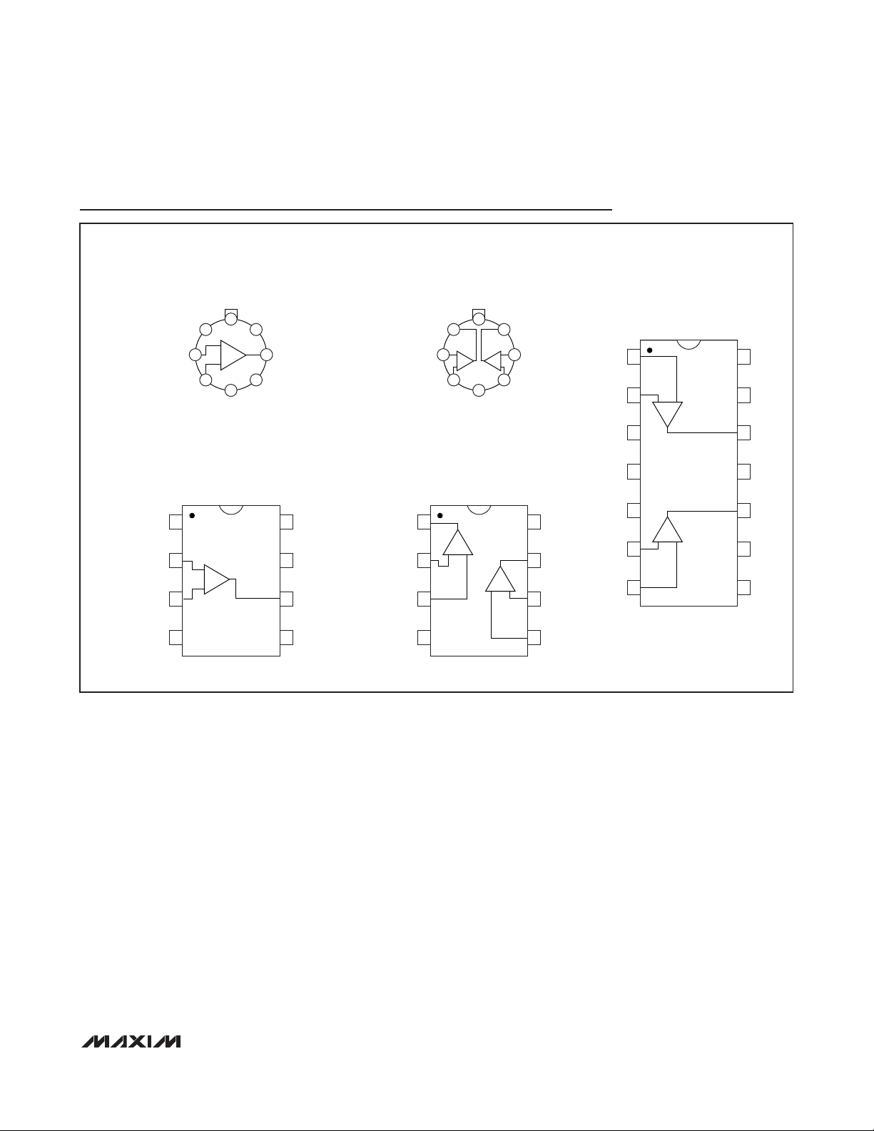
Pin Configurations
TOP VIEW SINGLES—ICL7611/12/14/16
OFFSET
1
OFFSET
-IN
2
3
+IN
4
V-
TO—99
SET)*
(I
O
8
1
-IN
3
+IN
4
V-
*PIN 7 CONNECTED TO CASE
8 LEAD
7
5
V+
OUTPUT
62
OFFSET
DUALS—ICL7621/22
TO—99
V+
8
4
V-
7
5
B
+-
62
+IN
OUT
B
-IN
B
B
V+
8
7
OUTB
6
-INB
5
+INB
1
-INA
+INA
2
312
OFFSETA
411
V-
510
OFFSETB
6
+INB
7
-INB
NOTE: PINS 9 & 13 ARE INTERNALLY CONNECTED
OUT
A
1
-IN
A
3
+IN
A
8 LEAD
SET)*
(I
8
O
7
V+
6
OUT
5
OFFSET
OUTA
-INA
+INA
1
A
-+
2
3
4
V-
14 LEAD
+-
A
B
+-
OFFSETA
14
13
V+
OUTA
N.C.
OUTB
9
V+
8
OFFSETB
*EXTERNAL COMPENSATION (ICL7614)
ICL761X–ICL764X
Single/Dual/Triple/Quad
Operational Amplifiers
4 _______________________________________________________________________________________
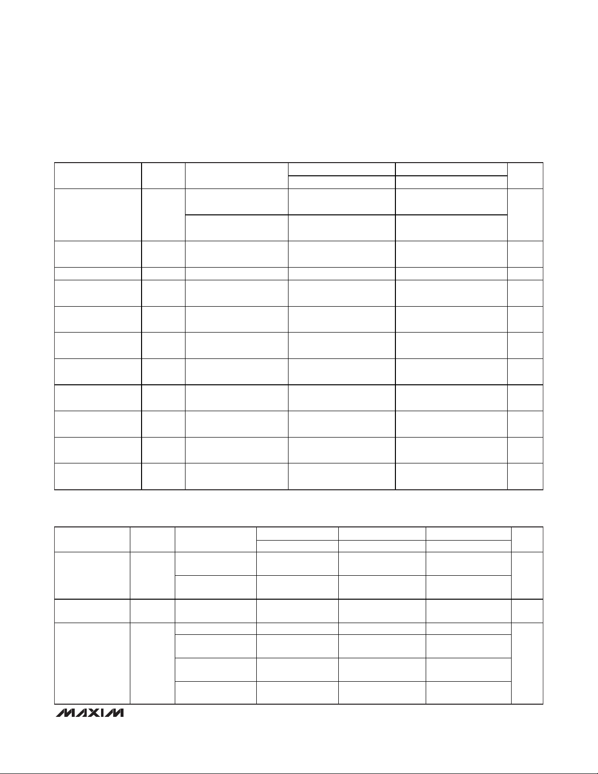
ABSOLUTE MAXIMUM RATINGS (Single/Dual)
ELECTRICAL CHARACTERISTICS (Single/Dual)
(V
SUPP
= ±1.0V, IQ= 10µA, TA= +25°C, unless otherwise noted.)
Stresses beyond those listed under “Absolute Maximum Ratings” may cause permanent damage to the device. These are stress ratings only, and functional
operation of the device at these or any other conditions beyond those indicated in the operational sections of the specifications is not implied. Exposure to
absolute maximum rating conditions for extended periods may affect device reliability.
Total Supply Voltage (V+ to V-) ...........................................+18V
Input Voltage ........................................(V+ + 0.3V) to (V- - 0.3V)
Differential Input Voltage (Note 1)......±(V+ + 0.3V) to (V- - 0.3V)
Duration of Output Short Circuit (Note 2) ......................Unlimited
Continuous Power Dissipation (T
A
= +25°C)
TO-99 Metal Can (derate 2mW/°C above +25°C) .......250mW
8-Pin Minidip (derate 2mW/°C above +25°C)..............250mW
14-Pin Plastic (derate 3mW/°C above +25°C) .............375mW
14-Pin CERDIP (derate 4mW/°C above +25°C)...........500mW
16-Pin Plastic (derate 3mW/°C above +25°C) .............375mW
16-Pin CERDIP (derate 4mW/°C above +25°C)...........500mW
Operating Temperature Ranges:
M Series.............................................................-55°C to +125°C
E Series................................................................-40°C to +85°C
C Series .................................................................-0°C to +70°C
Storage Temperature Range ............................-55°C to +150°C
Lead Temperature (soldering, 10s) ................................+300°C
Soldering Temperature (reflow)
Lead(Pb)-Free Packages.............................................+260°C
Packages Containing Lead..........................................+240°C
Note 1: Long-term offset voltage stability will be degraded if large input differential voltages are applied for long periods of time.
Note 2: The outputs may be shorted to ground or to either supply for V
SUPP
≤ 10V. Care must be taken to insure that the dissipation
rating is not exceeded.
PARAMETER SYMBOL CONDITIONS
RS ≤ 100kΩ,
T
= +25°C
Input Offset Voltage V
Temperature
Coefficient of V
Input Offset Current I
Input Bias Current I
Common-Mode
Voltage Range
(Except ICL7612/
ICL7616)
OS
ΔVOS/ΔTRS ≤ 100kΩ 10 15 µV/°C
V
OS
OS
BIAS
CMR
A
RS ≤ 100kΩ,
≤ TA ≤ T
T
MIN
TA = +25°C 0.5 30 0.5 30
0°C ≤ TA ≤ +70°C 300 300
TA = +25°C 1.0 50 1.0 50
0°C ≤ TA ≤ +70°C 500 500
MAX
ICL76XXA ICL76XXB
MIN TYP MAX MIN TYP MAX
25
37
-0.4 +0.6 -0.4 +0.6 V
UNITS
mV
pA
pA
Extended CommonMode Voltage Range
(ICL7612 Only)
Extended CommonMode Voltage Range
(ICL7616 Only)
Output Voltage Swing V
V
V
CMR
CMR
OUT
-1.1 +0.6 -1.1 +0.6 V
IQ = 10µA -1.3 -0.3 -1.3 -0.3 V
RL = 1MΩ, TA = +25°C ±0.98 ±0.98
RL = 1MΩ, 0°C ≤ TA ≤
+70°C
±0.96 ±0.96
V
ICL761X–ICL764X
Single/Dual/Triple/Quad
Operational Amplifiers
_______________________________________________________________________________________ 5
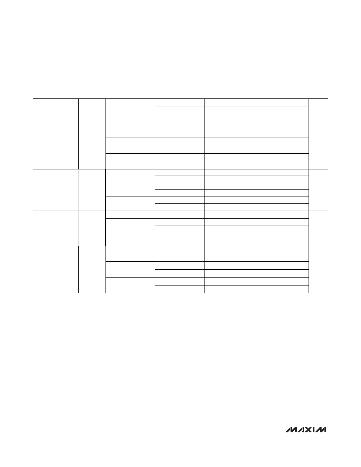
ELECTRICAL CHARACTERISTICS (Single/Dual) (continued)
(V
SUPP
= ±1.0V, IQ= 10µA, TA= +25°C, unless otherwise noted.)
ELECTRICAL CHARACTERISTICS (Single/Dual)
(V
SUPP
= ±5.0V, TA= +25°C, unless otherwise noted.)
PARAMETER SYMBOL CONDITIONS
VO = ±0.1V, RL = 1MΩ,
= +25°C
T
Large-Signal Voltage
Gain
Unity-Gain
Bandwidth
A
VOL
GBW 0.044 0.044 MHz
Input Resistance R
Common-Mode
Rejection Ratio
Power-Supply
Rejection Ratio
Input-Referred Noise
Voltage
Input-Referred Noise
Current
Supply Current (Per
Amplifier)
CMRR R
PSRR R
e
i
I
SUPP
Slew Rate SR
Rise Time t
Overshoot Factor
IN
n
n
r
A
VO = ±0.1V, RL = 1MΩ,
0°C ≤ T
≤ +70°C
A
≤ 100kΩ 80 80 dB
S
≤ 100kΩ 80 80 dB
S
RS = 100Ω, f = 1kHz 100 100 nV/√Hz
RS = 100Ω, f = 1kHz 0.01 0.01 pA/√Hz
No signal, no load 6 15 6 15 µA
A
= 1, CL = 100pF,
VOL
V
= 0.2V
IN
V
= 50mV, CL = 100pF,
IN
R
= 1MΩ
L
V
= 50mV, CL = 100pF,
IN
R
= 1MΩ
L
, RL = 1MΩ
P-P
ICL76XXA ICL76XXB
MIN TYP MAX MIN TYP MAX
90 90
80 80
12
10
0.016 0.016 V/µs
20 20 µs
55%
10
UNITS
dB
12
Ω
PARAMETER SYMBOL CONDITIONS
RS ≤ 100kΩ,
= +25°C
T
Input Offset
Voltage
Temperature
Coefficient of V
Input Offset
Current
V
OS
∆VOS/∆TRS ≤ 100kΩ 10 15 25 µV/°C
OS
I
OS
A
RS ≤ 100kΩ,
≤ TA ≤ T
T
MIN
TA = +25°C 0.5 30 0.5 30 0.5 30
C: 0°C ≤ TA ≤
+70°C
E: -40°C ≤ TA ≤
+85°C
M: -55°C≤ TA ≤
+125°C
MAX
ICL76XXA ICL76XXB ICL76XXD
MIN TYP MAX MIN TYP MAX MIN TYP MAX
UNITS
2515
mV
3720
300 300 300
800 800 800
800 800 800
pA
ICL761X–ICL764X
Single/Dual/Triple/Quad
Operational Amplifiers
6 _______________________________________________________________________________________
ELECTRICAL CHARACTERISTICS (Single/Dual) (continued)
(V
SUPP
= ±5.0V, TA= +25°C, unless otherwise noted.)
PARAMETER SYMBOL CONDITIONS
TA = +25°C 1.0 50 1.0 50 1.0 50
C: 0°C ≤ TA ≤
+70°C
Input Bias Current I
Common-Mode
Voltage Range
(Except ICL7612/
ICL7616)
Extended
Common-Mode
Voltage Range
(ICL7612 Only)
Extended
Common-Mode
Voltage Range
(ICL7616 Only)
V
V
V
BIAS
CMR
CMR
CMR
E: -40°C ≤ TA ≤
+85°C
M: -55°C≤ TA ≤
+125°C
IQ = 10µA (Note 3)
IQ = 100µA (Note 3)
IQ = 1mA (Note 3)
IQ = 10µA ±5.3 ±5.3 ±5.3
IQ = 100µA
IQ = 1mA
IQ = 10µA
IQ = 100µA
IQ = 1mA
ICL76XXA ICL76XXB ICL76XXD
MIN TYP MAX MIN TYP MAX MIN TYP MAX
400 400 400
4000 4000 4000
4000 4000 4000
+4.4 +4.4 +4.4
-4.0 -4.0 -4.0
+4.2 +4.2 +4.2
-4.0 -4.0 -4.0
+3.7 +3.7 +3.7
-3.7 -3.7 -3.7
+5.3 +5.3 +5.3
-5.1 -5.1 -5.1
+5.3 +5.3 +5.3
-4.5 -4.5 -4.5
-5.3 -5.3 -5.3
+3.7 +3.7 +3.5
-5.1 -5.1 -5.1
+3.0 +3.0 +2.7
-4.5 -4.5 -4.5
+2.0 +2.0 +1.7
UNITS
pA
V
V
V
ICL761X–ICL764X
Single/Dual/Triple/Quad
Operational Amplifiers
_______________________________________________________________________________________ 7
ELECTRICAL CHARACTERISTICS (Single/Dual) (continued)
(V
SUPP
= ±5.0V, TA= +25°C, unless otherwise noted.)
PARAMETER SYMBOL CONDITIONS
I
Q =
10µA,
RL =
1MΩ
(Note 3)
I
Output Voltage
Swing
V
OUT
Q =
100µA,
RL =
100kΩ
TA =
+25°C
C: 0°C ≤
≤
T
A
+70°C
E: -40°C
≤ T
≤
A
+85°C
M: -55°C
≤ TA ≤
+125°C
TA =
+25°C
C: 0°C ≤
T
≤
A
+70°C
E: -40°C
≤ T
≤
A
+85°C
ICL76XXA ICL76XXB ICL76XXD
MIN TYP MAX MIN TYP MAX MIN TYP MAX
±4.9 ±4.9 ±4.9
±4.8 ±4.8 ±4.8
±4.7 ±4.7 ±4.7
±4.7 ±4.7 ±4.7
±4.9 ±4.9 ±4.9
±4.8 ±4.8 ±4.8
±4.5 ±4.5 ±4.5
UNITS
V
M: -55°C
≤
≤ T
A
+125°C
TA =
+25°C
C: 0°C ≤
T
≤
I
Q =
1mA, RL
= 10kΩ
(Note 3)
A
+70°C
E: -40°C
≤ T
A
+85°C
M: -55°C
≤ T
A
+125°C
±4.5 ±4.5 ±4.5
±4.5 ±4.5 ±4.5
±4.3 ±4.3 ±4.3
≤
±4.0 ±4.0 ±4.0
±4.0 ±4.0 ±4.0
≤
ICL761X–ICL764X
Single/Dual/Triple/Quad
Operational Amplifiers
8 _______________________________________________________________________________________
(
)
ELECTRICAL CHARACTERISTICS (Single/Dual) (continued)
(V
SUPP
= ±5.0V, TA= +25°C, unless otherwise noted.)
PARAMETER SYMBOL CONDITIONS
VO =
±4.0V
RL =
1MΩ,
I
=
Q
10µA
TA =
+25°C
C: 0°C ≤
≤
T
A
+70°C
E: -40°C
≤ T
≤
A
+85°C
M: -55°C
≤
≤ T
A
+125°C
ICL76XXA ICL76XXB ICL76XXD
MIN TYP MAX MIN TYP MAX MIN TYP MAX
86 104 80 104 80 104
80 75 75
74 68 68
74 68 68
UNITS
Large-Signal
Voltage Gain A
VOL
V
O =
±4.0V,
RL =
100kΩ,
I
Q =
100µA
V
O =
±4.0V,
RL =
10kΩ,
I
Q =
1mA
Note 3
TA =
+25°C
C: 0°C ≤
T
≤
A
+70°C
E: -40°C
≤
≤ T
A
+85°C
M: -55°C
≤ T
≤
A
+125°C
TA =
+25°C
C: 0°C ≤
T
≤
A
+70°C
E: -40°C
≤ T
≤
A
+85°C
M: -55°C
≤
≤ T
A
+125°C
86 102 80 102 80 102
80 75 75
dB
74 68 68
74 68 68
80 83 76 83 76 83
76 72 72
72 68 68
72 68 68
ICL761X–ICL764X
Single/Dual/Triple/Quad
Operational Amplifiers
_______________________________________________________________________________________ 9
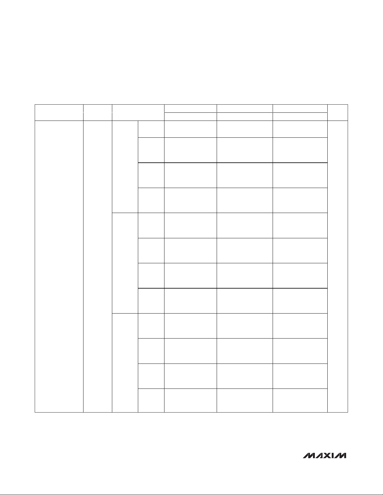
ELECTRICAL CHARACTERISTICS (Single/Dual) (continued)
(V
SUPP
= ±5.0V, TA= +25°C, unless otherwise noted.)
PARAMETER SYMBOL CONDITIONS
Unity-Gain
Bandwidth
Input Resistance R
Common-Mode
Rejection Ratio
Power-Supply
Rejection Ratio
Input-Referred
Noise Voltage
Input-Referred
Noise Current
GBW
CMRR
PSRR
e
IQ = 10µA (Note 3) 0.044 0.044 0.044
IQ = 100µA 0.48 0.48 0.48
= 1mA (Note 3) 1.4 1.4 1.4
I
Q
IN
RS ≤ 100kΩ,
= 10µA (Note 3)
I
Q
RS ≤ 100kΩ,
= 100µA
I
Q
≤ 100kΩ,
R
S
= 1mA (Note 3)
I
Q
RS ≤ 100kΩ,
I
= 10µA (Note 3)
Q
RS ≤ 100kΩ,
I
= 100µA
Q
R
≤ 100kΩ,
S
I
= 1mA (Note 3)
Q
RS = 100Ω, f =
n
1kHz
RS = 100Ω, f =
i
n
1kHz
ICL76XXA ICL76XXB ICL76XXD
MIN TYP MAX MIN TYP MAX MIN TYP MAX
12
10
76 96 70 96 70 96
76 91 70 91 70 91
66 87 60 87 60 87
80 94 80 94 80 94
80 86 80 86 80 86
70 77 70 77 70 77
100 100 100 nV/√Hz
0.01 0.01 0.01 pA/√Hz
10
UNITS
MHz
12
10
12
Ω
dB
dB
Supply Current
(Per Amplifier)
Channel
Separation
IQ = 10µA
(Note 3)
No
I
SUPP
V
O1
/ VO2A
signal,
no load
VOL
IQ =
100µA
= 1mA
I
Q
(Note 3)
= 100 120 120 120 dB
0.01 0.02 0.01 0.02 0.01 0.02
0.1 0.25 0.1 0.25 0.1 0.25
1.0 2.5 1.0 2.5 1.0 2.5
mA

ICL761X–ICL764X
Single/Dual/Triple/Quad
Operational Amplifiers
10 ______________________________________________________________________________________
ELECTRICAL CHARACTERISTICS (Single/Dual) (continued)
(V
SUPP
= ±5.0V, TA= +25°C, unless otherwise noted.)
Note 3: ICL7611, ICL7612, ICL7616 only.
Note 4: ICL7814; 39pF from pin 6 to pin 8.
PARAMETER SYMBOL CONDITIONS
=
A
VOL
=
1, C
Slew Rate
(Note 4)
SR
L
100pF,
V
=
IN
8V
P-P
IQ = 10µA
(Note 3),
R
= 1MΩ
L
IQ =
100µA, R
= 100kΩ
IQ = 1mA
(Note 3),
R
=
L
10kΩ
IQ = 10µA
(Note 3),
R
= 1MΩ
L
L
ICL76XXA ICL76XXB ICL76XXD
MIN TYP MAX MIN TYP MAX MIN TYP MAX
0.016 0.016 0.016
0.16 0.16 0.16
1.6 1.6 1.6
20 20 20
UNITS
V/µs
V
=
IN
Rise Time
(Note 4)
Overshoot Factor
(Note 4)
50mV,
t
r
C
=
L
100pF
V
=
IN
50mV,
C
=
L
100pF
IQ =
100µA, R
= 100kΩ
I
= 1mA
Q
(Note 3),
R
=
L
10kΩ
IQ = 10µA
(Note 3),
R
= 1MΩ
L
IQ =
100µA, R
= 100kΩ
I
= 1mA
Q
(Note 3),
R
=
L
10kΩ
L
L
22 2
0.9 0.9 0.9
55 5
10 10 10
40 40 40
µs
%

ICL761X–ICL764X
Single/Dual/Triple/Quad
Operational Amplifiers
______________________________________________________________________________________ 11
Pin Configurations
Ordering Information (Triple/Quad)
PART TEMP RANGE PIN-PACKAGE
ICL763XBCPE 0°C to +70°C 16 Plastic Dip
ICL763XBCSE 0°C to +70°C 16 Slim SO
ICL763XCCPE 0°C to +70°C 16 Plastic Dip
ICL763XCCSE 0°C to +70°C 16 Slim SO
ICL763XECPE 0°C to +70°C 16 Plastic Dip
ICL763XECSE 0°C to +70°C 16 Slim SO
ICL763XBCJE 0°C to +70°C 16 CERDIP
ICL763XCCJE 0°C to +70°C 16 CERDIP
ICL763XECJE 0°C to +70°C 16 CERDIP
ICL763XBMJE
16 CERDIP
ICL763XCMJE
16 CERDIP
PART TEMP RANGE PIN-PACKAGE
ICL764XBCPD
0°C to +70°C 14 Plastic Dip
ICL764XBCWE
0°C to +70°C 16 Wide SO
ICL764XCCPD 0°C to +70°C 14 Plastic Dip
ICL764XCCWE
0°C to +70°C 16 Wide SO
ICL764XECPD 0°C to +70°C 14 Plastic Dip
ICL764XECWE
0°C to +70°C 16 Wide SO
ICL764XBCJD 0°C to +70°C 14 CERDIP
ICL764XCCJD 0°C to +70°C 14 CERDIP
ICL764XECJD 0°C to +70°C 14 CERDIP
ICL764XBMJD
14 CERDIP
ICL764XCMJD
14 CERDIP
Note: X above is replaced by 1, 2.
-55°C to +125°C
-55°C to +125°C
TOP VIEW
ICL7631/32
16 LEAD
-55°C to +125°C
-55°C to +125°C
ICL7641/42
16 LEAD WIDE S.O.
ICL7641/42
14 LEAD
1
N.C.
-INA
2
A
+
314
+INA
413
OUTB
512
V+
6
SET I
OC
710
-INC
8
+INC
NOTE: PINS 5 & 15 ARE INTERNALLY CONNECTED
+
B
-
C
+
IOC SET
16
15
V+
OUTA
+INB
-INB
11
I
OB
OUT
9
V-
SET
1
OUTA
A
-INA
2
314
+INA
413
V+
512
INB
6
-INB
B
710
OUTB
N.C.
8
+-
+-
D
+-
+-
C
OUTD
16
15
-IND
+IND
V-
+INC
11
-INC
OUTC
9
N.C.
1
OUTA
A
-INA
2
314
+INA
413
V+
512
INB
611
-INB
B
710
OUTB
+-
+-
D
+-
+-
C
OUTD
16
15
-IND
+IND
V-
+INC
-INC
OUTC

ICL761X–ICL764X
Single/Dual/Triple/Quad
Operational Amplifiers
12 ______________________________________________________________________________________
ABSOLUTE MAXIMUM RATINGS (Triple/Quad)
ELECTRICAL CHARACTERISTICS (Triple/Quad)
(V
SUPP
= ±1.0V, IQ= 10µA, TA= +25°C, unless otherwise noted.) (Specifications apply to ICL7631/7632/7642 only.)
Stresses beyond those listed under “Absolute Maximum Ratings” may cause permanent damage to the device. These are stress ratings only, and functional
operation of the device at these or any other conditions beyond those indicated in the operational sections of the specifications is not implied. Exposure to
absolute maximum rating conditions for extended periods may affect device reliability.
Total Supply Voltage (V+ to V-) ...........................................+18V
Input Voltage ........................................(V+ + 0.3V) to (V- - 0.3V)
Differential Input Voltage (Note 5).......±|(V+ + 0.3V) - (V- - 0.3V)
Duration of Output Short Circuit (Note 6) ......................Unlimited
Continuous Power Dissipation (T
A
= +25°C)
TO-99 Metal Can (derate 2mW/°C above +25°C) .......250mW
8-Pin Minidip (derate 2mW/°C above +25°C)..............250mW
14-Pin Plastic (derate 3mW/°C above +25°C) .............375mW
14-Pin CERDIP (derate 4mW/°C above +25°C)...........500mW
16-Pin Plastic (derate 3mW/°C above +25°C) .............375mW
16-Pin CERDIP (derate 4mW/°C above +25°C)...........500mW
Operating Temperature Ranges:
M Series.............................................................-55°C to +125°C
E Series................................................................-40°C to +85°C
C Series .................................................................-0°C to +70°C
Storage Temperature Range ............................-55°C to +150°C
Lead Temperature (soldering, 10s) ................................+300°C
Note 5: Long-term offset voltage stability will be degraded if large input differential voltages are applied for long periods of time.
Note 6: The outputs may be shorted to ground or to either supply for V
SUPP
≤ 10V. Care must be taken to insure that the
dissipation rating is not exceeded.
PARAMETER SYMBOL CONDITIONS
Input Offset Voltage V
Temperature
Coefficient of V
Input Offset Current I
Input Bias Current I
Common-Mode
Voltage Range
Output Voltage
Swing
Large-Signal Voltage
Gain
Unity-Gain
Bandwidth
Input Resistance R
Common-Mode
Rejection Ratio
OS
∆VOS/∆TRS ≤ 100kΩ 15 20 µV/°C
RS ≤ 100kΩ,
T
= +25°C
OS
OS
BIAS
V
CMR
V
OUT
A
VOL
GBW 0.044 0.044 MHz
IN
CMRR R
A
RS ≤ 100kΩ,
≤ TA ≤ T
T
MIN
TA = +25°C 0.5 30 0.5 30
0°C ≤ TA ≤ +70°C 300 300
TA = +25°C 1.0 50 1.0 50
0°C ≤ TA ≤ +70°C 500 500
RL = 1MΩ, TA = +25°C ±0.98 ±0.98
RL = 1MΩ, 0°C ≤ TA ≤
+70°C
VO = ±0.1V, RL = 1MΩ,
= +25°C
T
A
V
= ±0.1V, R
O
0°C ≤ T
≤ 100kΩ 80 80 dB
S
≤ +70°C
A
MAX
= 1MΩ,
L
ICL76XXB ICL76XXC
MIN TYP MAX MIN TYP MAX
510
712
-0.4 +0.6 -0.4 +0.6 V
±0.96 ±0.96
90 90
80 80
10
12
10
12
UNITS
mV
pA
pA
V
dB
Ω

ICL761X–ICL764X
Single/Dual/Triple/Quad
Operational Amplifiers
______________________________________________________________________________________ 13
ELECTRICAL CHARACTERISTICS (Triple/Quad) (continued)
(V
SUPP
= ±1.0V, IQ= 10µA, TA= +25°C, unless otherwise noted.) (Specifications apply to ICL7631/7632/7642 only.)
ELECTRICAL CHARACTERISTICS (Triple/Quad)
(V
SUPP
= ±5.0V, TA= +25°C, unless otherwise noted.)
PARAMETER SYMBOL CONDITIONS
Power-Supply
Rejection Ratio
Input-Referred Noise
Voltage
Input-Referred Noise
Current
Supply Current (Per
Amplifier)
Channel Separation VO1 / VO2A
Slew Rate SR
Rise Time t
Overshoot Factor
PSRR 80 80 dB
e
I
SUPP
i
RS = 100Ω, f = 1kHz 100 100 nV/√Hz
n
RS = 100Ω, f = 1kHz 0.01 0.01 pA/√Hz
n
No signal, no load 6 15 6 15 µA
= 100 120 120 dB
VOL
A
= 1, CL = 100pF,
VOL
= 0.2V
V
IN
V
r
IN
100pF, R
V
IN
100pF, R
P-P
= 50mV, CL =
= 1MΩ
L
= 50mV, CL =
= 1MΩ
L
, RL = 1MΩ
ICL76XXB ICL76XXC
MIN TYP MAX MIN TYP MAX
0.016 0.016 V/µs
20 20 µs
55%
PARAMETER SYMBOL CONDITIONS
RS ≤ 100kΩ,
= +25°C
T
Input Offset
Voltage
Temperature
Coefficient of V
Input Offset
Current
Input Bias Current I
∆VOS/∆TRS ≤ 100kΩ 15 20 30 µV/°C
OS
V
OS
I
OS
BIAS
A
RS ≤ 100kΩ,
≤ TA ≤ T
T
MIN
TA = +25°C 0.5 30 0.5 30 0.5 30
C: 0°C ≤ TA ≤
+70°C
M: -55°C≤ TA ≤
+125°C
TA = +25°C 1.0 50 1.0 50 1.0 50
C: 0°C ≤ TA ≤
+70°C
M: -55°C≤ TA ≤
+125°C
MAX
ICL76XXB ICL76XXC ICL76XXE
MIN TYP MAX MIN TYP MAX MIN TYP MAX
51020
71525
300 300 300
800 800 800
500 500 500
4000 4000 4000
UNITS
UNITS
mV
pA
pA

ICL761X–ICL764X
Single/Dual/Triple/Quad
Operational Amplifiers
14 ______________________________________________________________________________________
ELECTRICAL CHARACTERISTICS (Triple/Quad) (continued)
(V
SUPP
= ±5.0V, TA= +25°C, unless otherwise noted.)
PARAMETER SYMBOL CONDITIONS
IQ = 10µA (Note 7)
Common-Mode
Voltage Range
V
CMR
IQ = 100µA (Note 9)
IQ = 1mA (Note 8)
IQ =
10µA,
R
=
L
1MΩ
(Note 7)
TA =
+25°C
C: 0°C ≤
≤
T
A
+70°C
M: -55°C
≤ T
≤
A
+125°C
ICL76XXB ICL76XXC ICL76XXE
MIN TYP MAX MIN TYP MAX MIN TYP MAX
+4.4 +4.4 +4.4
-4.0 -4.0 -4.0
+4.2 +4.2 +4.2
-4.0 -4.0 -4.0
+3.7 +3.7 +3.7
-3.7 -3.7 -3.7
±4.9 ±4.9 ±4.9
±4.8 ±4.8 ±4.8
±4.7 ±4.7 ±4.7
UNITS
V
Output Voltage
Swing
V
OUT
IQ =
100µA,
R
=
L
100kΩ
(Note 9)
IQ =
1mA, R
= 10kΩ
(Note 8)
L
TA =
+25°C
C: 0°C ≤
≤
T
A
+70°C
M: -55°C
≤ T
≤
A
+125°C
TA =
+25°C
C: 0°C ≤
≤
T
A
+70°C
M: -55°C
≤ T
≤
A
+125°C
±4.9 ±4.9 ±4.9
±4.8 ±4.8 ±4.8
±4.5 ±4.5 ±4.5
±4.5 ±4.5 ±4.5
±4.3 ±4.3 ±4.3
±4.0 ±4.0 ±4.0
V

ICL761X–ICL764X
Single/Dual/Triple/Quad
Operational Amplifiers
______________________________________________________________________________________ 15
ELECTRICAL CHARACTERISTICS (Triple/Quad) (continued)
(V
SUPP
= ±5.0V, TA= +25°C, unless otherwise noted.)
PARAMETER SYMBOL CONDITIONS
VO =
±4.0V,
R
=
L
1MΩ,
=
I
Q
10µA
(Note 7)
VO =
±4.0V,
Large-Signal
Voltage Gain
A
VOL
R
=
L
100kΩ,
I
=
Q
100µA
V
=
O
±4.0V,
=
R
L
10kΩ
(Note 8),
I
=
Q
1mA
(Note 7)
TA =
+25°C
C: 0°C ≤
≤
T
A
+70°C
M: -55°C
≤ T
≤
A
+125°C
TA =
+25°C
C: 0°C ≤
≤
T
A
+70°C
M: -55°C
≤
≤ T
A
+125°C
TA =
+25°C
C: 0°C ≤
≤
T
A
+70°C
M: -55°C
≤
≤ T
A
+125°C
ICL76XXB ICL76XXC ICL76XXE
MIN TYP MAX MIN TYP MAX MIN TYP MAX
86 104 80 104 80 104
80 75 75
74 68 68
86 102 80 102 80 102
80 75 75
74 68 68
86 98 80 98 80 98
80 75 75
74 68 68
UNITS
dB

ICL761X–ICL764X
Single/Dual/Triple/Quad
Operational Amplifiers
16 ______________________________________________________________________________________
ELECTRICAL CHARACTERISTICS (Triple/Quad) (continued)
(V
SUPP
= ±5.0V, TA= +25°C, unless otherwise noted.)
PARAMETER SYMBOL CONDITIONS
IQ = 10µA (Note 7) 0.044 0.044 0.044
Unity-Gain
Bandwidth
G
IQ = 100µA (Note 9) 0.48 0.48 0.48
BW
IQ = 1mA (Note 8) 1.4 1.4 1.4
Input Resistance R
IN
RS ≤ 100kΩ,
= 10µA (Note 7)
I
Q
Common-Mode
Rejection Ratio
CMRR
Power-Supply
Rejection Ratio
Input-Referred
Noise Voltage
Input-Referred
Noise Current
PSRR
RS ≤ 100kΩ,
I
= 100µA
Q
R
≤ 100kΩ,
S
I
= 1mA (Note 8)
Q
RS ≤ 100kΩ,
I
= 10µA (Note 7)
Q
RS ≤ 100kΩ,
I
= 100µA
Q
R
≤ 100kΩ,
S
I
= 1mA (Note 8)
Q
RS = 100Ω, f = 1kHz 100 100 100 nV/√Hz
e
n
RS = 100Ω, f = 1kHz 0.01 0.01 0.01 pA/√Hz
i
n
IQ = 10µA
(Note 7)
Supply Current
(Per Amplifier)
I
SUPP
No
signal,
no load
IQ =
100µA
I
(Note 8)
Channel
Separation
V
O1
/ VO2A
= 100 120 120 120 dB
VOL
IQ = 10µA
(Note 7),
VOL
IN
P-P
=
=
L
=
R
L
IQ = 100µA,
R
L
IQ = 1mA
Slew Rate
(Note 10)
SR
A
1, C
100pF,
V
8V
(Note 7),
R
L
= 1mA
Q
= 1MΩ
= 100kΩ
= 10kΩ
ICL76XXB ICL76XXC ICL76XXE UNITS
MIN TYP MAX MIN TYP MAX MIN TYP MAX
12
10
76 96 70 96 70 96
76 91 70 91 70 91
66 87 60 87 60 87
80 94 80 94 80 94
80 86 80 86 80 86
70 77 70 77 70 77
0.01 0.022 0.01 0.022 0.01 0.022
0.1 0.25 0.1 0.25 0.1 0.25
1.0 2.5 1.0 2.5 1.0 2.5
0.016 0.016 0.016
0.16 0.16 0.16
1.6 1.6 1.6
10
MHz
12
10
12
Ω
dB
dB
mA
V/µs

ICL761X–ICL764X
Single/Dual/Triple/Quad
Operational Amplifiers
______________________________________________________________________________________ 17
ELECTRICAL CHARACTERISTICS (Triple/Quad) (continued)
(V
SUPP
= ±5.0V, TA= +25°C, unless otherwise noted.)
Note 7: Does not apply to ICL7641.
Note 8: Does not apply to ICL7642.
Note 9: ICL7631/ICL7632 only.
Note 10: Does not apply to ICL7632.
Typical Operating Characteristics
(TA = +25°C, unless otherwise noted.)
PARAMETER SYMBOL CONDITIONS
V
=
Rise Time
(Note 10)
Overshoot Factor
(Note 10)
t
r
IN
50mV,
C
=
L
100pF
=
V
IN
50mV,
C
=
L
100pF
IQ = 10µA
(Note 7),
R
= 1MΩ
L
IQ = 100µA,
R
= 100kΩ
L
= 1mA
I
Q
(Note 8),
R
= 10kΩ
L
IQ = 10µA
(Note 7),
R
= 1MΩ
L
IQ = 100µA,
R
= 100kΩ
L
= 1mA
I
Q
(Note 8),
R
= 10kΩ
L
ICL76XXB ICL76XXC ICL76XXE
MIN TYP MAX MIN TYP MAX MIN TYP MAX
20 20 20
222
0.9 0.9 0.9
555
10 10 10
40 40 40
UNITS
µs
%

ICL761X–ICL764X
Single/Dual/Triple/Quad
Operational Amplifiers
18 ______________________________________________________________________________________
Typical Operating Characteristics (continued)
(TA = +25°C, unless otherwise noted.)
ICL761X–ICL764X
Single/Dual/Triple/Quad
Operational Amplifiers
______________________________________________________________________________________
19
Typical Operating Characteristics (continued)
(TA = +25°C, unless otherwise noted.)
ICL761X–ICL764X
Single/Dual/Triple/Quad
Operational Amplifiers
20 ______________________________________________________________________________________
Typical Operating Characteristics (continued)
(TA = +25°C, unless otherwise noted.)

ICL761X–ICL764X
Single/Dual/Triple/Quad
Operational Amplifiers
______________________________________________________________________________________ 21
Detailed Description
Quiescent Current Selection
The voltage input to the IQpin of the single and triple
amplifiers selects a quiescent current (I
Q
) of 10µA,
100µA, or 1000µA. The dual and quad amplifiers have
fixed quiescent current (IQ) settings. Unity-gain bandwidth and slew-rate increase with increasing quiescent
current, as does output sink current capability. The output source current capability is independent of quiescent current.
The lowest I
Q
setting that results in sufficient bandwidth
and slew rate should be selected for each specific
application.
The IQpin of the single and triple amplifiers controls
the quiescent current as follows:
Input Offset Nulling
The input offset can be nulled by connecting a 25kΩ
pot between the OFFSET terminals with the wiper connected to V+. At quiescent currents of 1mA and 100µA,
the nulling range provided is adequate for all V
OS
selections. However, with higher values of VOS, and an
IQof 10µA, nulling may not be possible.
Frequency Compensation
All of the ICL7611 and ICL7621 series except the
ICL7614 are internally compensated for unity-gain
operation. The ICL7614 is externally compensated by a
capacitor connected between COMP and OUT pins,
with 39pF being greater than unity. The compensation
capacitor value may be reduced to increase the bandwidth and slew rate. The ICL7132 is not compensated
and does not have frequency compensation pins. Use
only at gains 20 at IQof 1mA; at gains > 10 at IQof
100µA; at gain > 5 at IQof 10µA.
Output Loading Considerations
Approximately 70% of the amplifier’s quiescent current
flows in the output stage. The output swing can
approach the supply rails for output loads of 1MΩ,
100kΩ, and 10kΩ, using the output stage in a highly
linear Class A mode. Crossover distortion is avoided
and the voltage gain is maximized in this mode. The
output stage, however, can also be operated in Class
AB, which supplies higher output currents (see the
Typical Operating Characteristics
). The voltage gain
decreases and the output transfer characteristic is nonlinear during the transition from Class A to Class B
operation.
The output stage, with a gain that is directly proportional to load impedance, approximates a transconductance amplifier. Approximately the same open-loop
gains are obtained at each of the IQsettings if corresponding loads of 10kΩ, 100kΩ, and 1MΩ are used.
The maximum output source current is higher than the
maximum sink current, and is independent of IQ.
Like most amplifiers, there are output loads for which
the amplifier stability is not guaranteed. In particular,
avoid capacitive loads greater than 100pF; and while
on the 1mA IQsetting, avoid loads less than 5kΩ. Since
the output stage is a transconductance output, very
large (>10µF) capacitive loads will create a dominant
pole and the output will be stable, even with loads that
are less than 5kΩ.
Extended Common-Mode Voltage Range
(ICL7612/ICL7616)
A common-mode voltage range that includes both V+
and V- is often desirable, especially in single-supply
operation. The ICL7612/ICL7616 extended commonmode range op amps are designed specifically to meet
this need. The ICL7612 input common-mode voltage
range (CMVR) extends beyond both power-supply rails
when operated with at least 3V total supply and an I
Q
of 10µA or 100µA. The ICL7616 CMVR includes the
negative supply voltage (or ground when operated with
a single supply) at an IQor 10µA or 100µA.
PC Board Layout
Careful PC board layout techniques must be used to
take full advantage of the very low bias current of the
ICL7611 family. The inputs should be encircled with a
low-impedance trace, or guard, that is at the same
potential as the inputs. In an inverting amplifier, this is
normally ground; in a unity-gain buffer connect the
guard to the output. A convenient way of guarding the
8-pin TO-99 version of the ICL7611 is to use a 10-pin
circle, with the two extra pads on either side of the
input pins to provide space for a guard ring (see Figure
8). Assembled boards should be carefully cleaned,
and if a high humidity environment is expected, conformally coated.
IQ= 10µA IQpin to V+
I
Q
= 100µA IQpin between V- + 0.8V and V+ - 0.8V
I
Q
= 1mA IQpin to V-
ICL761X–ICL764X
Single/Dual/Triple/Quad
Operational Amplifiers
22 ______________________________________________________________________________________
Single-Supply Operation
The ICL7611 family will operate from a single 2V to 16V
power supply. The common-mode voltage range of the
standard amplifier types when operated from a single
supply is 1.0V to (V+ - 0.6V) at 10µA I
Q
. At 100µA IQ,
the CMVR is 1.0V to (V+ - 0.8V), and at 1mA IQ, the
CMVR is 1.3V to (V+ - 1.3V). If this CMVR range is
insufficient, use the ICL7612, whose CMVR includes
both ground and V+, or the ICL7616, whose CMVR
includes ground.
A convenient way to generate a psuedo-ground at V+/2
is to use one op amp of a quad to buffer a V+/2 voltage
from a high-impedance resistive divider.
Low-Voltage Operation
Operation at V
SUPP
= ±1.0V is only guaranteed at IQ=
10µA. Output swings to within a few millivolts of the
supply rails are achievable for RL(> or =) 1MΩ.
Guaranteed input CMVR is ±0.6V minimum and typically +0.9V to -0.7V at V
SUPP
= ±1.0V. For applications
where greater common-mode range is desirable, see
the description of ICL7612 and ICL7616 above.
Applications Information
Note that in no case is IQ shown. The value of IQ must
be chosen by the designer with regard to frequency
response and power dissipation.
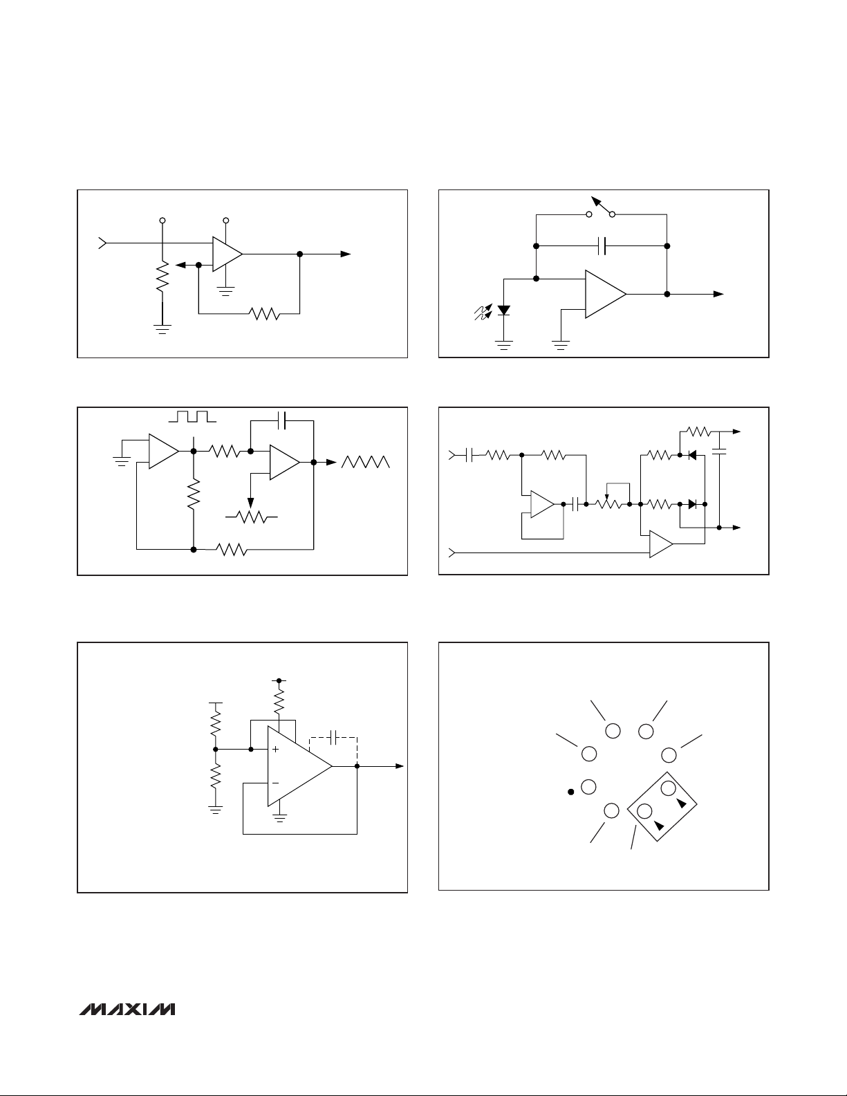
Figure 1. Instrumentation Amplifier—Adjust R3 to improve
CMRR. The offset of all three amplifiers is nulled by the offset
adjustment of A2.
Figure 2. Simple Follower—By using the ICL7612 in these
applications, the circuits will follow rail-to-rail inputs
+
R1
V
IN
+18V
+
-
A1
R2
R2
25kΩ
R
R
R3
A3
+
R3
V
IN
V
OUT
+
ICL7612
-
RL ≥ 10kΩ
V
OUT
A2
+
R3R2R2
GAIN = ( +1
)
R1
ICL761X–ICL764X
Single/Dual/Triple/Quad
Operational Amplifiers
______________________________________________________________________________________ 23
Figure 3. Level Detector—By using the ICL7612 in these applications, the circuits will follow rail-to-rail inputs.
Figure 4. Photocurrent Integrator—Low-leakage currents allow
integration times up to several hours.
Figure 5. Precise Triangle/Square Wave Generator—The frequency and duty cycle are virtually independent of power supply.
Figure 6. Averaging AC to DC Converter—Recommended for
Maxim’s ICL7106/ICL7107/ICL7109 A/D Converters.
Figure 7. Burn-In and Life Test Circuit
Figure 8. Input Guard for TO-99
+5 +5
V
IN
100kΩ
V
+
OUT
TO CMOS OR
LPTTL LOGIC
1MΩ
-
+
1
⁄2
ICL7621
1MΩ
-
+
1MΩ
ICL7621
V- V+
DUTY CYCLE
880kΩ
1
⁄2
IH5040
1µF
+-
-
ICL7611
V
OUT
+
0.05µF
V
IN
COMMON
10kΩ
2.2MΩ 20kΩ
10µF
+
-
ICL7621
1
⁄
2
1.8kΩ = 5%
SCALE
ADJUST
20kΩ
-
+
1
⁄
2
ICL7621
1MΩ
V
ON
TO
SUCCEEDING
INPUT
STAGE
V
OL
+15V
+15V
10kΩ
NOTES:
1. ICL7611, 7612, 7616, 7631, 7632
2. ICL7611, 7612, 7616, 7621, 7622, 7631, 7641, 7642
10kΩ
100Ω
NOTE 1
V+
I
O
COMP
OUT
V-
NOTE 2
BOTTOM VIEW
OUTPUT
V+
7
6
5
4
V
SET
I
O
8
1
2
3
INPUTS
GUARD
ICL761X–ICL764X
Single/Dual/Triple/Quad
Operational Amplifiers
24 ______________________________________________________________________________________
Figure 9. Low Droop Rate Sample and Hold—S2 improves
accuracy and acquisition time by including the voltage drop
across S1 inside the feedback loop. R1 closes the feedback
loop of A1 during the hold phase. The droop rate is [I
BIAS(AZ
)
+ I
LEAK(S1
) + I
LEAK(S2)
]/C
HOLD
.
Figure 10. Long-Time Constant Integrator—With RIN= 1011
Ω
,
the time constant of this integrator is 100,000s. Since the input
voltage is converted to a current by R
IN
, the input voltage can
far exceed the power-supply range.
Figure 11. Pico Ammeter—The response time of this curcuit is
R
FB
x CFB, where CFBis the stray capacitance between the
output and the inverting terminal of the amplifier.
Figure 12. 60Hz Twin “T“ Notch Filter—The low 1pA bias current of the ICL7611 allows use of small 540pF and 270pF
capacitors, even with a notch frequency of 60Hz. The 60Hz
rejection is approximately 40dB.
Typical Operating Circuit
S/H
CONTROL
INPUT
C
1µF
INT
100kΩ
R
1
1
⁄
2
ICL7622
A1
V
IN
S1
IH5141
S2
C
ICL7622
HOLD
1
⁄
2
A2
CURRENT
SOURCE
C
RFB - 1011Ω
-
+
FB
V
O
= 100mV/pA
R
IN
V
IN
V
OUT
-
+
V
OUT
V
IN
540pF
5MΩ
10MΩ10MΩ
-
+
OUTPUT
ICL7611
270pF270pF
C
INT
R
IN
V
IN
LONG TIME CONSTANT INTEGRATOR
(Detailed Circuit Diagram — Figure 10)
-
+
V
OUT
ICL761X–ICL764X
Single/Dual/Triple/Quad
Operational Amplifiers
______________________________________________________________________________________ 25
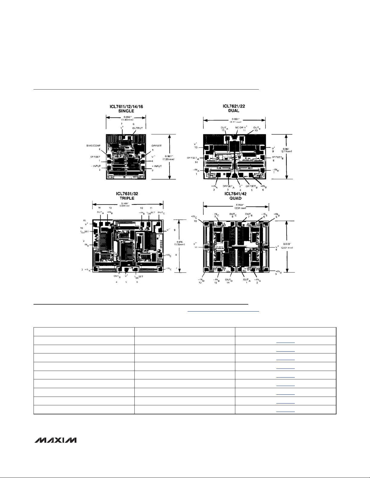
Chip Topographies
Package Information
For the latest package outline information and land patterns, go to www.maxim-ic.com/packages. Note that a “+”, “#”, or “-” in the
package code indicates RoHS status only. Package drawings may show a different suffix character, but the drawing pertains to the
package regardless of RoHS status.
PACKAGE TYPE PACKAGE CODE DOCUMENT NO.
TO99 T99-8
21-0022
8 PDIP P8-1
21-0043
8 SO S8-2
21-0041
8 CDIP J16-3
21-0045
14 PDIP P14-3
21-0043
14 CDIP J14-3
21-0045
16 PDIP P16-1
21-0043
16 SO S16-1
21-0041
16 Wide SO W16-2
21-0042

Revision History
ICL761X–ICL764X
Single/Dual/Triple/Quad
Operational Amplifiers
Maxim cannot assume responsibility for use of any circuitry other than circuitry entirely embodied in a Maxim product. No circuit patent licenses are
implied. Maxim reserves the right to change the circuitry and specifications without notice at any time.
26
____________________Maxim Integrated Products, 120 San Gabriel Drive, Sunnyvale, CA 94086 408-737-7600
© 2010 Maxim Integrated Products Maxim is a registered trademark of Maxim Integrated Products, Inc.
REVISION
NUMBER
2 4/08 Removed all part numbers offered in die form from the Ordering Information 2, 11
3 5/10 Corrected letter grades in EC table headings 13–17
REVISION
DATE
DESCRIPTION
PAGES
CHANGED
 Loading...