

Page 1

DS89C420 Ultra High
-
Speed
www.maxim
-
ic.com
Microcontroller User’s Guide
SECTION 1: INTRODUCTION
The Dallas Semiconductor DS89C420 is an 8051-compatible microcontroller that provides improved
performance and power consumption when compared to the original 8051 version. It retains instruction
set and object code compatibility with the 8051, yet performs the same operations in fewer clock cycles.
Consequently, greater throughput is possible for the same crystal speed. As an alternative, the DS89C420
can be run at a reduced frequency to save power. The more effic ient design allows a much slower crystal
speed to get the same results as an original 8051, using much less power.
The fundamental innovation of the DS89C420 is the use of only one clock per instruction cycle compared
with twelve for the original 8051. This results in up to 12 times improvement in performance over the
original 8051 architecture and up to 4 times improvement over other Dallas Semiconductor High-Speed
Microcontrollers. The DS89C420 provides several peripherals and features in addition to all of the
standard features of an 80C32. These include 16KB of on-chip flash memory, 1KB of on-chip RAM, 4
eight bit I/O ports, three 16-bit timer/counters, two on-chip UARTs, dual data pointers, an on-chip
watchdog timer, 5 levels of interrupt priority, and a crystal multiplier. The device provides 256 bytes of
RAM for variables and stack. 128 bytes can be reached using direct or indirect addressing and 128 using
only indirect addressing.
In addition to improved efficiency, the DS89C420 can operate at a maximum clock rate of 33 MHz.
Combined with the 12 times performance, this allows for a maximum performance of 33 MIPs. This
level of computing power is comparable to many 16-bit processors, but without the added expense and
complexity if implementing a 16-bit interface.
The DS89C420 incorporates a Power Management Mode which allows the device to dynamically vary
the internal clock speed from 1 clock per cycle (default) to 1024 clocks per cycle. Because power
consumption is directly proportional to clock speed, the device can reduce its operating frequency during
periods of little or no activity. This greatly reduces power consumption. The switch-back feature allows
the device to quickly return to highest speed operation upon receipt of an interrupt or serial port activity,
allowing the device to respond to external events while in Power Management Mode.
1 of 192 020602
Page 2

DS89C420 Ultra High-Speed Microcontroller User’s Guide
SECTION 2: ORDERING INFORMATION
The DS89C420 family follows the part numbering convention shown below. Note that not all
combinations of devices may be currently available. Contact a Maxim / Dallas Semiconductor Sales
Office for up to date details.
DS89C420-QCL
SPEED: L 33 MHz
TEMPERATURE: C 0 °C to 70 °C
N -40 °C to 85 °C
PACKAGE: M PDIP
Q PLCC
E Thin Quad Flat Pack (TQFP)
OPERATING VOLTAGE: 0 +5V
MEMORY TYPE: 9 Flash
2 of 192
Page 3

DS89C420 Ultra High-Speed Microcontroller User’s Guide
SECTION 3:ARCHITECTURE
The DS89C420 Architecture is based on the industry standard 87C52 and executes the standard 8051
instruction set. The core is an accumulator based architecture using internal registers for data storage and
peripheral control. This section provides a brief description of each architecture feature. Details
concerning the programming model, instruction set, and register description are provided in Section 4.
ALU
The ALU is responsible for math functions, comparisons, and general decision making in the DS89C420.
The ALU is not explicitly used by software. Instruction decoding prepares the ALU automatically and
passes it the appropriate data. The ALU primarily uses two special function registers (SFRs) as the
source and destination for all operations. These are the Accumulator and B register. The ALU also
provides status information in the Program Status Register. The SFRs are described below.
SPECIAL FUNCTION REGISTERS
All peripherals and operations that are not explicitly controlled by instructions in the DS89C420 are
controlled via Special Function Registers (SFRs). All SFRs are described in Section 4. The most
commonly used registers that are basic to the architecture are also described below.
Accumulator
The Accumulator is the primary register used in the DS89C420. It is a source and destination for many
operations involving math, data movement, and decisions. Although it can be bypassed, most high-speed
instructions require the use of the Accumulator (A or ACC) as one argument.
B Register
The B register is used as the second 8-bit argument in multiply and divide operations. When not used for
these purposes, the B register can be used as a general purpose register.
Program Status Word
The Program Status Word holds a selection of bit flags that include the Carry Flag, Auxiliary Carry Flag,
General Purpose Flag, Register Bank Select, Overflow Flag, and Parity Flag.
Data Pointer(s)
The Data Pointers (DPTR and DPTR1) are used to assign a memory address for the MOVX instructions.
This address can point to a data memory location, either on- or off-chip, or a memory mapped peripheral.
When moving data from one memory area to another or from memory to a memory mapped peripheral, a
pointer is needed for both the source and destination. The user can select the active pointer via a
dedicated SFR bit (Sel =DPS.0), or can activate an automatic toggling feature for altering the pointer
selection (TSL=DPS.5). An additional feature if selected, provides automatic incrementing or
decrementing of the current DPTR.
Stack Pointer
The Stack Pointer denotes the register location at the top of the Stack, which is the last used value. The
user can place the Stack anywhere in the scratchpad RAM by setting the Stack Pointer to the desired
location, although the lower bytes are normally used for working registers.
2 of 192
Page 4

DS89C420 Ultra High-Speed Microcontroller User’s Guide
I/O Ports
The DS89C420 offers four 8-bit I/O ports. Each I/O port is represent ed by an SFR location, and can be
written or read. The I/O port has a latch that contains the value written by software. In general, software
reads the state of external pins during a read operation.
Timer/Counters
Three 16-bit Timer/Counters are available in the DS89C420. Each timer is contained in two SFR
locations that can be written or read by software. The timers are controlled by other SFRs described in
Section 4.
UARTs
The DS89C420 provides two UARTs which are controlled and accessed by SFRs. Eac h UART has an
address that is used to read and write the UART. The same address is used for both read and write
operations, and the read and write operations are distinguished by the instruction. Each UART is
controlled by its own SFR control register.
SCRATCHPAD REGISTERS (RAM)
The High-Speed Core provides 256 bytes of Scratchpad RAM for general purpose data and variable
storage. The first 128 bytes are directly available to software. The second 128 are available through
indirect addressing discussed below. Selected portions of this RAM have other optional functions.
Stack
The stack is a RAM area that the DS89C420 uses to store return address information during Calls and
Interrupts. The user can also place variables on the stack when necessary. The Stack Pointer designates
the RAM location that is the top of the stack. Thus, depending on the value of the Stack Pointer, the
stack can be located anywhere in the 256 bytes of RAM. A common location would be in the upper 128
bytes of RAM, as these locations are accessible through indirect addressing only.
Working Registers
The first thirty-two bytes of the Scratchpad RAM can be used as four banks of eight Working Registers
for high speed data movement. Using four banks, software can quickly change cont ext by simply
changing to a different bank. In addition to the Accumulator, the Working Registers are commonly used
as data source or destination. Some of the Working Registers can also be used as pointers to other RAM
locations (indirect addressing).
PROGRAM COUNTER
The Program Counter (PC) is a 16-bit value that designates the next program address to be fetched. Onchip hardware automatically increments the PC value to move to the next ROM location.
ADDRESS/DATA BUS
The DS89C420 addresses a 64KB program and 64KB data memory area which resides in a combination
of internal and external memory. When external memory is accessed, Ports 0 and 2 are used as a
multiplexed address and data bus. The DS89C420 supports three external memory bus structures. The
non-page mode (traditional 8051) bus structure provides the address MSB on Port 2 and multiplexes Port
0 between address LSB and data. The page mode 1 bus structure uses Port 0 exclusively for data and
3 of 192
Page 5

DS89C420 Ultra High-Speed Microcontroller User’s Guide
multiplexes Port 2 between address MSB and address LSB. The page mode 2 bus structure uses Port 0
exclusively for address LSB and multiplexes Port 2 between address MSB and data. These addressing
modes are detailed later in the User Guide.
WATCHDOG TIMER
The Watchdog Timer provides a supervisory function for applications that cannot afford to run out of
control. The Watchdog Timer is a programmable free running timer. If allowed to reach the termination
of its count, if enabled, the Watchdog will reset the CPU. Software must prevent this by clearing or
resetting the Watchdog prior to its time-out.
POWER MONITOR
The DS89C420 incorporates a band -gap reference and analog circuitry to monitor the power supply
conditions. When VCC begins to drop out of tolerance, the Power Monitor will issue an optional ea rly
warning Power-fail interrupt. If power continues to fall, the Power Monitor will invoke a reset condition.
This will remain until power returns to normal operating voltage. The Power Monitor also functions on
power-up, holding the microcontroller in a reset state until power is stable.
INTERRUPTS
The DS89C420 is capable of evaluating thirteen interrupt sources simultaneously. Each interrupt has an
associated interrupt vector, flag, priority, and enable. These interrupts can be globally enabled or
disabled.
TIMING CONTROL
The DS89C420 provides an on-chip oscillator for use with an external crystal. This can be bypassed by
injecting a clock source into the XTAL 1 pin. The clock source is used to create machine cycle timing
(four clocks), ALE, PSEN, Watchdog, Timer, and serial baud rate timing. In addition, an on-chip ring
oscillator can be used to provide an approximately 10 MHz clock source. A frequency multiplier feature
is included which can be selected by SFR control to multiply the input clock source by either 2 or 4. This
allows lower frequency (and cost) crystals to be used while still allowing internal operation up to the full
33 MHz limit.
FLASH MEMORY
On-chip program memory is impemented in 16KB of Flash Memory. This can be programmed in system
with the standard 5 volt V
port (in-system) using a built-in program memory Loader (ROM Loader) or by a standard Flash or
EPROM programmer. Full programming details are given in Section 15.
The DS89C420 incorporates a Memory Management Unit (MMU) and other hardware to support any of
the three programming methods. The MMU controls program and data memory access, and provides
sequencing and timing controls for programming of the on-chip program memory. There is also a
separate Security Flash block which is used to support a standard three-level lock, a 64-byte encryption
array and other Flash options.
The full on-chip program memory range can be fetched by the processor automatically. Reset routines
and all interrupt vectors are located in the lower 128 bytes of the on-chip program memory area.
supply under the control of the user software (in-application), or via a serial
CC
4 of 192
Page 6

DS89C420 Ultra High-Speed Microcontroller User’s Guide
SECTION 4: PROGRAMMING MODEL
This section provides a programmer’s overview of the Ultra High-Speed Microcontroller core. It
includes information on the memory map, on-chip RAM, Special Function Registers (SFRs), and
instruction set. The programming model of the Ultra High-Speed Microcontroller is very similar to that
of the industry standard 80C52. The memory map is identical. It uses the same instruction set, with
improved instruction timing. Several new SFRs have been added.
MEMORY ORGANIZATION
The Ultra High-Speed Microcontroller, like the 8052, uses several distinct memory areas. These areas
include Registers, program memory, and data memory. Registers serve to control on-chip peripherals and
as RAM. Note that registers (on-chip RAM) are separate from data memory. Registers are divided into
three categories including directly addressed on-chip RAM, indirectly addressed on-chip RAM, and
Special Function Registers. The program and data memory areas are discussed under Memory Map. The
Registers are discussed under Register Map.
MEMORY MAP
The Ultra High-Speed Microcontroller uses a memory addressing scheme that separates program memory
from data memory. Each area is 64KB beginning at address 0000h and ending at FFFFh as shown in
Figure 4-1. The program and data segments can overlap since they are accessed in different ways.
Program memory is fetched by the microcontroller automatically. These addresses are never written by
software. In fact, there are no instructions that allow the program area to be written. There is one
instruction (MOVC) that is used to explicitly read the program area. This is commonly used to read lookup tables. The data memory area is accessed explicitly using the MOVX instruction. This instruction
provides multiple ways of specifying the target address. It is used to access the 64KB of data memory.
The address and data range of devices with on-chip program and data memory overlap the 64K memory
space. When on-chip memory is enabled, accessing memory in the on-chip range will cause the device to
access internal memory. Memory accesses beyond the internal range will be addressed externally via
ports 0 and 2.
The ROMSIZE feature allows software to dynamically configure the maximum address of on-chip
program memory. This allows the device to act as a bootstrap loader for an external Flash or Nonvolatile
SRAM. Secondly, this method can also be used to increase the amount of available program memory
from 64KB to 80KB without bank switching. For more information on this feature, please consult
Section 6.
Program and data memory can also be increased beyond the 64KB limit using bank switching techniques.
This is described in Application Note 81, Memory Expansion with the High-Speed Microcontroller
family.
REGISTER MAP
The Register Map is illustrated in Figure 4-2. It is entirely separate from the program and data memory
areas mentioned above. A separate class of instructions is used to access the registers. There are 256
potential register location values. In practice, the Ultra High-Speed Microcontroller has 256 bytes of
Scratchpad RAM and up to 128 Special Function Registers (SFRs). This is possible since the upper 128
Scratchpad RAM locations can only be accessed indirectly. That is, the contents of a Working Register
(R0 or R1) or the stack pointer (described below) will designate the RAM location. A direct reference to
one of the lower 128 addresses (0-7Fh) will access the Scratchpad RAM. A direct reference to one of the
5 of 192
Page 7

DS89C420 Ultra High-Speed Microcontroller User’s Guide
PROGRAM
DATA
upper 128 addresses (80h - FFh) must be an SFR access. In contrast, indirect references can access the
entire Scratchpad RAM range (0h-FFh).
Scratchpad RAM is available for general purpose data storage. It is commonly used in place of off-chip
RAM when the total data contents are small. When off-chip RAM is needed, the Scratchpad area will
still provide the fastest general purpose access. Within the 256 bytes of RAM, there are several special
purpose areas. These are described as follows:
Bit Addressable Locations
In addition to direct register access, some individual bits are also accessible. These are individually
addressable bits in both the RAM and SFR area. In the Scratchpad RAM area, registers 20h to 2Fh are
bit addressable. This provides 128 (16 * 8) individual bits available to software. A bit access is
distinguished from a full register access by the type of instruction. Addressing modes are discussed later
in this section. In the SFR area, any register location ending in a 0 or 8 is bit addressable. Figure 4-3
shows details of the on-chip RAM addressing including the locations of individual RAM bits.
Working Registers
As part of the lower 128 bytes of RAM, there are four banks of Working Registers (8 bytes each). The
Working registers are general purpose RAM locations that can be addressed in a special way. They are
designated R0 through R7. Since there are four ba nks, the currently selected bank will be used by any
instruction using R0-R7. This allows software to change context by simply switching banks. This is
controlled via the Program Status Word register in the SFR area described below. The Working Registers
also allow their contents to be used for indirect addressing of the upper 128 bytes of RAM. Thus an
instruction can designate the value stored in R0 (for example) to address the upper RAM. This value
might be the result of another calculation.
Stack
Another use of the Scratchpad area is for the programmer’s stack. This area is selected using the Stack
Pointer (SP;81h) SFR. Whenever a call or interrupt is invoked, the return address is placed on the Stack.
It also is available to the programmer for variables, etc. since the Stack can be moved, there is no fixed
location within the RAM designated as Stack. The Stack Pointer will default to 07h on reset. The user
can then move it as needed. A convenient location would be the upper RAM area (>7Fh) since this is
only available indirectly. The SP will point to the last used value. Therefore, the next value placed on
the Stack is put at SP + 1. Each PUSH or CALL will increment the SP by the appropriate value. Each
POP or RET will decrement as well.
MEMORY MAP Figure 4-1
0000h
MEMORY
MEMORY
64K FFFFh
6 of 192
Page 8
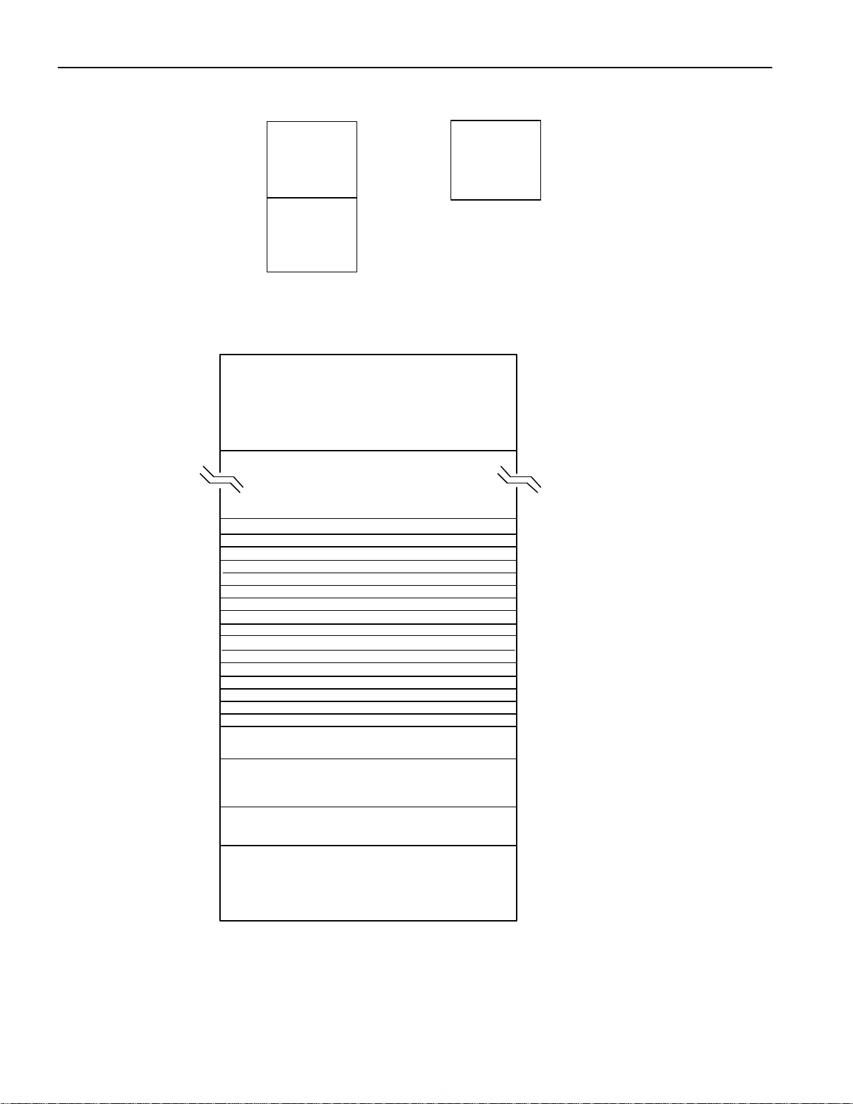
DS89C420 Ultra High-Speed Microcontroller User’s Guide
FFh
DIRECT
INDIRECT
DIRECT
REGISTER MAP Figure 4-2
FFh
RAM
7Fh
255
128
SPECIAL
FUNCTION
REGISTERS
FFh
7Fh
0000h
RAM
SCRATCHPAD REGISTER ADDRESSING Figure 4-3
INDIRECT RAM
7Fh
DIRECT RAM
2Fh 7F 7E 7D 7C 7B 7A 79 78
2Eh 77 76 75 74 73 72 71 70
2Dh 6F 6E 6D 6C 6B 6A 69 68
2Ch 67 66 65 64 63 62 61 60
2Bh 5F 5E 5D 5C 5B 5A 59 58
2Ah 57 56 55 54 53 52 51 50
29h 4F 4E 4D 4C 4B 4A 49 48
28h 47 46 45 44 43 42 41 40
27h 3F 3E 3D 3C 3B 3A 39 38
26h 37 36 35 34 333 32 31 30
25h 2F 2E 2D 2C 2B 2A 29 28
24h 27 26 25 24 23 22 21 20
23h 1F 1E 1D 1C 1B 1A 19 18
22h 17 16 15 14 13 12 11 10
21h 0F 0E 0D 0C 0B 0A 09 08
20h 07 06 05 04 03 02 01 00
1Fh
BANK 3
18h
17h
BANK 2
10h
0Fh
BANK 1
08h
07h
BANK 0
00h
MSB LSB
7 of 192
Page 9

DS89C420 Ultra High-Speed Microcontroller User’s Guide
ADDRESSING MODES
The Ultra High-Speed Microcontroller uses the standard 8051 instruction set which is supported by a
wide range of third party assemblers and compilers. Like the 8051, the Ultra High-Speed Microcontroller
uses three memory areas. These are program memory, data memory, and Registers. The program and data
areas are 64KB each. They extend from 0000h to FFFFh. The register areas are located between 00h and
FFh, but do not overlap with the program and data segments. This is because the Ultra High-Speed
Microcontroller uses different modes of addressing to reach each memory segment. These modes are
described below.
Program memory is the area from which all instructions are fetched. It is inherently read only. This is
because the 8051 instruction set provides no instructions that write to this area. Read/write access is for
data memory and Registers only. No special action is required to fetch from program memory. Each
instruction fetch will be performed automatically by the on-chip CPU. In versions that contain on chip
memory, the hardware will decide whether the fetch is on-chip or off-chip based on the address. Explicit
addressing modes are needed for the data memory and register areas. These modes determine which
register area is accessed or if off-chip data memory is used.
The Ultra High-Speed Microcontroller supports eight addressing modes. They are:
Register Addressing
Direct Addressing
Register Indirect Addressing
Immediate Addressing
Register Indirect Addressing with Displacement
Relative Addressing
Page Addressing
Extended Ad dressing
Five of the eight are used to address operands. The remainder are used for program control and
branching. When writing assembly language instructions that use arguments, the convention is
destination, source. Each mode of addressing is summarized below. Note that many instructions (such as
ADD) have multiple addressing modes available.
8 of 192
Page 10

DS89C420 Ultra High-Speed Microcontroller User’s Guide
Register Addressing
Register Addressing is used for operands that are located in one of the eight Working Registers (R7 -R0).
The eight Working Registers can be located in one of four Working Register banks found in the lower 32
bytes of Scratchpad RAM, as determined by the current register bank select bits. A register bank is
selected using two bits in the Program Status Word (PSW;D0h). This addressing mode is powerful, since
it uses the active bank without knowing which bank is selected. Thus one instruction can have multiple
uses by simply switching banks. Register Addressing is also a high-speed instruction, requiring only one
machine cycle. Two examples of Register Addressing are provided below.
ADD A, R4 ;Add register R4 to Accumulator
INC R2 ;Increment the value in register R2
In the first case, the value in R4 is the source of the operation. In the later, R2 is the destination. These
instructions do not consider the absolute address of the register. They will act on whichever bank has
been selected.
Any Working Register may also be accessed by Direct Addressing, described below. To do this, the
absolute address must be specified.
Direct Addressing
Direct Addressing is the mode used to access the entire lower 128 bytes of Scratchpad RAM and the SFR
area. It is commonly used to move the value in one register to another. Two examples are shown below.
MOV 72h, 74h ;Move the value in register 74 to
;register 72.
MOV 90h, 20h ;Move the value in register 20 to
;the SFR at 90h (Port 1)
Note that there is no instruction difference between a RAM access and an SFR access. The SFRs are
simply register locations above 7Fh.
Direct Addressing also extends to bit addressing. There is a group of instructions that explicitly use bits.
The address information provided to such an instruction is the bit location, rather than the register
address. Registers between 20h and 2Fh contain bits that are individually addressable. SFRs that end in
0 or 8 are bit addressable. An example of Direct Bit Addressing is as follows.
SETB 00h ;Set bit 00 in the RAM. This is the
;LSb of the register at address 20h
;as shown earlier in this section.
MOV C, 0B7h ;Move the contents of bit B7 to the
;Carry flag. Bit B7 is the MSb of
;register B0 (Port 3).
9 of 192
Page 11

DS89C420 Ultra High-Speed Microcontroller User’s Guide
Register Indirect Addressing
This mode is used to access the Scratchpad RAM locations above 7Fh. It can also be used to reach the
lower RAM (0h - 7Fh) if needed. The address is supplied by the contents of the Working Register
specified in the instruction. Thus one instruction can be used to reach many values by altering the
contents of the designated Working Register. Note that in general, only R0 and R1 can be used as
pointers. An example of Register Indirect Addressing is as follows.
ANL A, @R0 ;Logical AND the Accumulator
;with the contents of the register
;pointed to by the value stored in R0.
This mode is also used for Stack manipulation. This is becaus e all Stack references are directed by the
value in the Stack Pointer register. The Push and Pop instructions use this method of addressing. An
example is as follows.
PUSH A ;Saves the contents of the
;accumulator on the stack.
Register Indirect Addressing is used for all off-chip data memory accesses. These involve the MOVX
instruction. The pointer registers can be R0, R1, DPTR0 and DPTR1. Both R0 and R1 reside in the
Working Register area of the Scratchpad RAM. They can be used to reference a 256 byte area of off-chip
data memory. When using this type of addressing, the upper address byte is supplied by the value in the
Port 2 latch. This value must be selected by software prior to the MOVX instruction. An example is as
follows.
MOVX @R0, A ;Write the value in the accumulator
;to the address pointed to by R0 in
;the page pointed to by P2.
The 16-bit Data pointers (DPTRs) can be used as an absolute off-chip reference. This gives access to the
entire 64KB data memory map. An example is as follows.
MOVX @DPTR, A ;Write the value in the accumulator
;to the address referenced by the
;selected data pointer.
Immediate Addressing
Immediate Addressing is used when one of the operands is predetermined and coded into the software.
This mode is commonly used to initialize SFRs and to mask particular bits without affecting others. An
example is as follows.
ORL A, #40h ;Logical OR the Accumulator with 40h.
10 of 192
Page 12

DS89C420 Ultra High-Speed Microcontroller User’s Guide
Register Indirect with Displacement
Register Indirect Addressing with Displacement is used to access data in lookup tables in program
memory space. The location is created using a base address with an index. The base address can be
either the PC or the DPTR. The index is the accumulator. The result is stored in the accumulator. An
example is as follows.
MOVC A, @A +DPTR ;Load the accumulator with the contents
of program memory
;pointed to by the contents of the DPTR
plus the value in
;the accumulator.
Relative Addressing
Relative Addressing is used to determine a destination address for Conditional branch. Each of these
instructions includes an 8-bit value that contains a two’s complement address offset (–127 to +128) which
is added to the PC to determine the destination address. This destination is branched to when the tested
condition is true. The PC points to the program memory location immediately following the branch
instruction when the offset is added. If the tested condition is not true, the next instruction is performed.
An example is as follows.
JZ $–20 ;Branch to the l ocation (PC+2)–20
;if the contents of the accumulator = 0.
Page Addressing
Page Addressing is used by the Branching instructions to specify a destination address within the same
2KB block as the next contiguous instruction. The full 16-bit address is calculated by taking the five
highest order bits for the next instruction (PC+2) and concatenating them with the lowest order 11 bit
field contained in the current instruction. An example is as follows.
0870h ACALL 100h ;Call to the subroutine at address 100h
plus the
;current page address.
In this example, the current page address is 800h, so the destination address is 900h.
Extended Addressing
Extended Addressing is used by the Branching instructions to specify a 16-bit destination address within
the 64KB address space. The destination address is fixed in software as an absolute value. An example
is as follows.
LJMP 0F732h ;Jump to address 0F732h.
11 of 192
Page 13

DS89C420 Ultra High-Speed Microcontroller User’s Guide
PROGRAM STATUS FLAGS
All Program Status Flags are contained in the Program Status Word at SFR location D0h. It contains
flags that reflect the status of the CPU and the result of selected operations. The flags are summarized
below. The following table shows the instructions that affect each flag.
Bit Description :
PSW.7 C
Carry Set when the previous operation resulted in a carry (during addition) or a
borrow (during subtraction), otherwise cleared.
PSW.6 AC
Auxiliary Carry Set when the previous operation resulted in a carry (during addition) or a
borrow (during subtraction) from the high orde r nibble. Otherwise cleared.
PSW.2 OV
Overflow For addition, set when a carry was generated into a high order bit (bit 6 or
bit 7), but not a carry out of the same high order bit. For subtraction, OV
set if a borrow is needed into a high order bit (b it 6 or bit 7), but not into the
other high order bit. For multiplication, OV is set when the product
exceeds FFh. For division, OV is always cleared.
PSW.0 P
Parity Set to logic 1 to indicate an odd number of ones in the accumulator (odd
parity). Cleared for an even number of ones. This produces even parity.
All of these bits are cleared to a logic 0 for all resets.
INSTRUCTIONS THAT AFFECT FLAG SETTINGS Table 4-1
INSTRUCTION FLAGS INSTRUCTION FLAGS
C OV AC C OV AC
ADD X X X CLR C 0
ADDC X X X CPL C X
SUBB X X X ANL C, bit X
MUL 0 X
DIV 0 X
DA X
RRC X MOV C, bit X
RLC X CJNE X
SETB C 1
ANL C, bit
ORL C, bit
ORL C, bit
X indicates the modification is according to the result of the instruction.
X
X
X
12 of 192
Page 14

DS89C420 Ultra High-Speed Microcontroller User’s Guide
SPECIAL FUNCTION REGISTERS
The DS89C420, like the 8051, uses Special Function Registers (SFRs) to control peripherals and modes.
In many cases, an SFR will control individual functions or report status on individual functions. The
SFRs reside in register locations 80h-FFh and are reached using direc t addressing. SFRs that end in 0 or
8 are bit addressable.
All standard SFR locations from the original 8051 are duplicated in the DS89C420, with several
additions. Tables are provided to illustrate the locations of the SFRs for the DS89C420 device and t he
default reset conditions of all SFR bits. Detailed descriptions of each Special Function Register follow.
13 of 192
Page 15
DS89C420 Ultra High-Speed Microcontroller User’s Guide
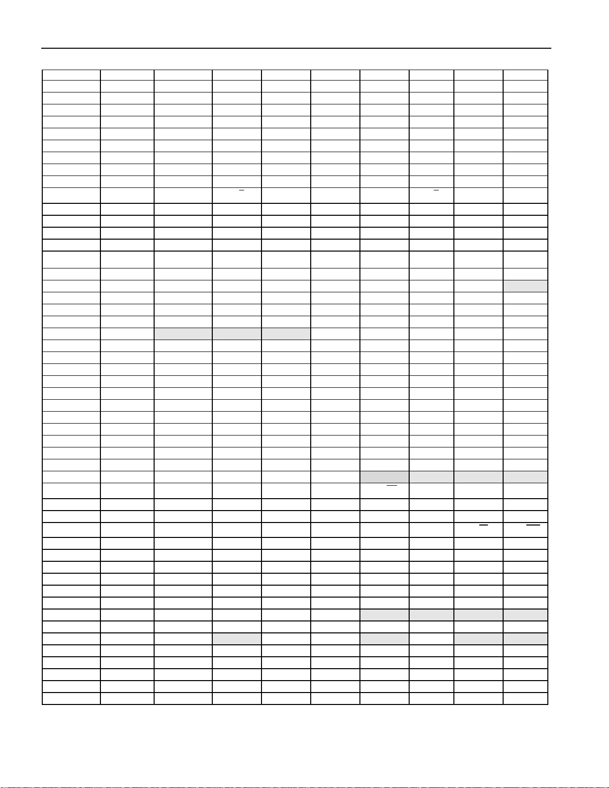
DS89C420 SPECIAL FUNCTION REGISTER LOCATIONS
REGISTER ADDRESS BIT 7 BIT 6 BIT 5 BIT 4 BIT 3 BIT 2 BIT 1 BIT 0
P0 80h P0.7 P0.6 P0.5 P0.4 P0.3 P0.2 P0.1 P0.0
SP 81h
DPL 82h
DPH 83h
DPL1 84h
DPH1 85h
DPS 86h ID1 ID0 TSL AID - - - SEL
PCON 87h SMOD_0 SMOD0 OFDF OFDE GF1 GF0 STOP IDLE
TCON 88h TF1 TR1 TF0 TR0 IE1 IT1 IE0 IT0
TMOD 89h GATE
TL0 8Ah
TL1 8Bh
TH0 8Ch
TH1 8Dh
CKCON 8Eh WD1 WD0 T2M T1M T0M MD2 MD1 MD0
P1 90h P1.7 P1.6 P1.5 P1.4 P1.3 P1.2 P1.1 P1.0
EXIF 91h IE5 IE4 IE3 IE2 CKRY RGMD RGSL BGS
CKMOD 96h
SCON0 98h SM0/FE_0 SM1_0 SM2_0 REN_0 TB8_0 RB8_0 TI_0 RI_0
SBUF0 99h
ACON 9Dh PAGEE PAGES1 PAGES0
P2 A0h P2.7 P2.6 P2.5 P2.4 P2.3 P2.2 P2.1 P2.0
IE A8h EA ES1 ET2 ES0 ET1 EX1 ET0 EX0
SADDR0 A9h
SADDR1 AAh
P3 B0h P3.7 P3.6 P3.5 P3.4 P3.3 P3.2 P3.1 P3.0
IP1 B1h - MPS1 MPT2 MPS0 MPT1 MPX1 MPT0 MPX0
IP0 B8h - LPS1 LPT2 LPS0 LPT1 LPX1 LPT0 LPX0
SADEN0 B9h
SADEN1 BAh
SCON1 C0h SM0/FE_1 SM1_1 SM2_1 REN_1 TB8_1 RB8_1 TI_1 RI_1
SBUF1 C1h
ROMSIZE C2h PRAME RMS2 RMS1 RMS0
PMR C4h CD1 CD0 SWB CTM
STATUS C5h PIS2 PIS1 PIS0 - SPTA1 SPRA1 SPTA0 SPRA0
TA C7h
T2CON
T2MOD C9h - - - - - - T2OE DCEN
RCAP2L CAh
RCAP2H CBh
TL2 CCh
TH2 CDh
PSW D0h CY AC F0 RS1 RS0 OV F1 P
FCNTL D5h FBUSY FERR FC3 FC2 FC1 FC0
FDATA D6h
WDCON D8h SMOD_1 POR EPFI PFI WDIF WTRF EWT RWT
ACC E0h
EIE E8h - - - EWDI EX5 EX4 EX3 EX2
B F0h
EIP1 F1h MPWDI MPX5 MPX4 MPX3 MPX2
EIP0 F8h - - - LPWDI LPX5 LPX4 LPX3 LPX2
C8h
TF2 EXF2 RCLK TCLK EXEN2 TR2 C/ T2 CP/ RL2
C/ T
T2MH T1MH T0MH
Shaded bits are Timed Access protected
M1 M0 GATE
4X/ 2X
C/ T
ALEON DME1 DME0
M1 M0
14 of 192
Page 16

DS89C420 Ultra High-Speed Microcontroller User’s Guide
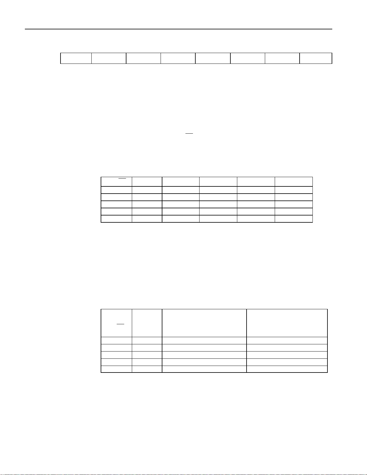
DS89C420 SPECIAL FUNCTION REGISTER RESET
VALUES
REGISTER ADDRESS BIT 7 BIT 6 BIT 5 BIT 4 BIT 3 BIT 2 BIT 1 BIT 0
P0 80h 1 1 1 1 1 1 1 1
SP 81h 0 0 0 0 0 1 1 1
DPL 82h 0 0 0 0 0 0 0 0
DPH 83h 0 0 0 0 0 0 0 0
DPL1 84h 0 0 0 0 0 0 0 0
DPH1 85h 0 0 0 0 0 0 0 0
DPS 86h 0 0 0 0 0 1 0 0
PCON 87h 0 0 Special Special 0 0 0 0
TCON 88h 0 0 0 0 0 0 0 0
TMOD 89h 0 0 0 0 0 0 0 0
TL0 8Ah 0 0 0 0 0 0 0 0
TL1 8Bh 0 0 0 0 0 0 0 0
TH0 8Ch 0 0 0 0 0 0 0 0
TH1 8Dh 0 0 0 0 0 0 0 0
CKCON 8Eh 0 0 0 0 0 0 0 1
P1 90h 1 1 1 1 1 1 1 1
EXIF 91h 0 0 0 0 Special Special Special 0
CKMOD 96h 1 1 0 0 0 1 1 1
SCON0 98h 0 0 0 0 0 0 0 0
SBUF0 99h 0 0 0 0 0 0 0 0
ACON 9Dh 0 0 0 1 1 1 1 1
P2 A0h 1 1 1 1 1 1 1 1
IE A8h 0 0 0 0 0 0 0 0
SADDR0 A9h 0 0 0 0 0 0 0 0
SADDR1 AAh 0 0 0 0 0 0 0 0
P3 B0h 1 1 1 1 1 1 1 1
IP1 B1h 1 0 0 0 0 0 0 0
IP0 B8h 1 0 0 0 0 0 0 0
SADEN0 B9h 0 0 0 0 0 0 0 0
SADEN1 BAh 0 0 0 0 0 0 0 0
SCON1 C0h 0 0 0 0 0 0 0 0
SBUF1 C1h 0 0 0 0 0 0 0 0
ROMSIZE C2h 1 1 1 1 0 1 0 1
PMR C4h 1 0 0 0 0 0 0 0
STATUS C5h 0 0 0 1 0 0 0 0
TA C7h 1 1 1 1 1 1 1 1
T2CON C8h 0 0 0 0 0 0 0 0
T2MOD C9h 1 1 1 1 1 1 0 0
RCAP2L CAh 0 0 0 0 0 0 0 0
RCAP2H CBh 0 0 0 0 0 0 0 0
TL2 CCh 0 0 0 0 0 0 0 0
TH2 CDh 0 0 0 0 0 0 0 0
PSW D0h 0 0 0 0 0 0 0 0
FCNTL D5h 1 0 1 1 0 0 0 0
FDATA D6h 0 0 0 0 0 0 0 0
WDCON D8h 0 Special 0 Special 0 Special Special 0
ACC E0h 0 0 0 0 0 0 0 0
EIE E8h 1 1 1 0 0 0 0 0
B F0h 0 0 0 0 0 0 0 0
EIP1 F1h 1 1 1 0 0 0 0 0
EIP0 F8h 1 1 1 0 0 0 0 0
15 of 192
Page 17

DS89C420 Ultra High-Speed Microcontroller User’s Guide
SPECIAL FUNCTION REGISTERS
Most of the unique features of the Ultra High-Speed Microcontroller family are controlled by bits in
special function registers (SFRs) located in unused locations in the 8051 SFR map. This allows for
increased functionality while maintaining complete instruction set compatibility.
The description for each bit indicates its read and write access, as well as its state after a power on reset.
Port 0 (P0)
7 6 5 4 3 2 1 0
SFR 80h P0.7 P0.6 P0.5 P0.4 P0.3 P0.2 P0.1 P0.0
P0.7-0
RW-1 RW-1 RW-1 RW-1 RW-1 RW-1 RW-1 RW-1
R=Unrestricted Read, W=Unrestricted Write, -n=Value after Reset
Port 0. This port functions according to the table below where PAGEE =
ACON.7 and PAGES = ACON.6-5
PAGEE PAGES Port0 Function
0 xx General Purpose I/0 (code execution < ROMSIZE.2-0)
0 xx Multiplexed Address LSB / Data (code execution > ROMSIZE.2-0)
1 00, 01, 10 Data
1 11 Address LSB
When serving as general purpose I/O, the port is open-drain and requires pullups. Writing a ‘1’ to one of the bits of this register configures the associated
port0 pin as an input. All read operations, with the exception of Read-ModifyWrite instructions, will leave the port latch unchange d. During external memory
addressing and data memory write cycles, the port has high and low drive
capability. During external memory data read cycles, the port will be held in a
high impedance state.
Stack Pointer (SP)
7 6 5 4 3 2 1 0
SFR 81h SP.7 SP.6 SP.5 SP.4 SP.3 SP.2 SP.1 SP.0
SP.7-0
Bits 7-0
RW-0 RW-0 RW-0 RW-0 RW-0 RW-1 RW-1 RW-1
R=Unrestricted Read, W=Unrestricted Write, -n=Value after Reset
Stack Pointer. This stack pointer is written by software to identify the location
where the stack will begin. The stack pointer is incremented before every PUSH
operation and is decremented following every POP operation. This register
defaults to 07h after reset.
16 of 192
Page 18

DS89C420 Ultra High-Speed Microcontroller User’s Guide
Data Pointer Low 0 (DPL)
7 6 5 4 3 2 1 0
SFR 82h PDL.7 PDL.6 PDL.5 PDL.4 PDL.3 PDL.2 PDL.1 PDL.0
RW-0 RW-0 RW-0 RW-0 RW-0 RW-0 RW-0 RW-0
R=Unrestricted Read, W=Unrestricted Write, -n=Value after Reset
DPL.7-0
Bits 7-0
Data Pointer Low 0. This register is the low byte of the standard 80C32 16-bit
data pointer. DPL and DPH are used to point to non-scratchpad data RAM.
Data Pointer High 0 (DPH)
7 6 5 4 3 2 1 0
SFR 83h DPH.7 DPH.6 DPH.5 DPH.4 DPH.3 DPH.2 DPH.1 DPH.0
DPH.7-0
Bits 7-0
RW-0 RW-0 RW-0 RW-0 RW-0 RW-0 RW-0 RW-0
R=Unrestricted Read, W=Unrestricted Write, -n=Value after Reset
Data Pointer High 0. This register is the high byte of the standard 80C32 16-bit
data pointer. DPL and DPH are used to point to non-scratchpad data RAM.
Data Pointer Low 1 (DPL1)
7 6 5 4 3 2 1 0
SFR 84h DPL1.7 DPL1.6 DPL1.5 DPL1.4 DPL1.3 DPL1.2 DPL1.1 DL1H.0
DPL1.7-0
Bits 7-0
Data Pointer High 1 (DPH1)
7 6 5 4 3 2 1 0
SFR 85h DPH1.7 DPH1.6 DPH1.5 DPH1.4 DPH1.3 DPH1.2 DPH1.1 DPH1.0
DPH1.7-0
Bits 7-0
RW-0 RW-0 RW-0 RW-0 RW-0 RW-0 RW-0 RW-0
R=Unrestricted Read, W=Unrestricted Write, -n=Value after Reset
Data Pointer Low 1. This register is the low byte of the auxiliary 16-bit data
pointer. When the SEL bit (DPS.0) is set, DPL1 and DPH1 are used in place of
DPL and DPH during DPTR operations.
RW-0 RW-0 RW-0 RW-0 RW-0 RW-0 RW-0 RW-0
R=Unrestricted Read, W=Unrestricted Write, -n=Value after Reset
Data Pointer High 1. This register is the high byte of the auxiliary 16-bit data
pointer. When the SEL bit (DPS.0) is set, DPL1 and DPH1 are used in place of
DPL and DPH during DPTR operations.
17 of 192
Page 19

DS89C420 Ultra High-Speed Microcontroller User’s Guide
Data Pointer Select (DPS)
7 6 5 4 3 2 1 0
SFR 86h ID1 ID0 TSL AID - - - SEL
ID1
Bit 7
RW-0 RW-0 RW-0 R-0 R-0 R-1 R-0 RW-0
R=Unrestricted Read, W=Unrestricted Write, -n=Value after Reset
Increment / Decrement Select for DPTR1. This bit determines the effect of
the INC DPTR instruction on DPTR1 when selected (SEL=1) as the active data
pointer.
0 = INC DPTR increments DPTR1 (default)
1 = INC DPTR decrements DPTR1
ID0
Bit 6
TSL
Bit 5
AID
Bit 4
Increment / Decrement Select for DPTR. This bit determines the effect of the
INC DPTR instruction on DPTR when selected (SEL=0) as the active data
pointer.
0 = INC DPTR increments DPTR (default)
1 = INC DPTR decrements DPTR
Toggle Select. When clear (=0), DPTR related instructions do not affect the
SEL bit. When set (=1), the SEL bit is toggled following execution of any of the
below DPTR related instructions:
INC DPTR
MOV DPTR, #data16
MOVC A, @A+DPTR
MOVX A, @DPTR
MOVX @DPTR, A
Auto Increment/Decrement Enable. When set, the active data pointer is
automatically incremented or decremented (as determined by ID1, ID0 bit
settings) following execution of any of the below DPTR related instructions:
MOVC A, @A+DPTR
MOVX A, @DPTR
MOVX @DPTR, A
Bits 3-1
SEL
Bit 0
Reserved. These bits will read 010b.
Data Pointer Select. This bit selects the active data pointer.
0 = Instructions that use the DPTR will use DPL and DPH.
1= Instructions that use the DPTR will use DPL1 and DPH1.
18 of 192
Page 20

DS89C420 Ultra High-Speed Microcontroller User’s Guide
Power Control (PCON)
7 6 5 4 3 2 1 0
SFR 87h SMOD_0 SMOD0 OFDF OFDE GF1 GF0 STOP IDLE
RW-0 RW-0 RW-0* RW-0* RW-0 RW-0 RW-0 RW-0
R=Unrestricted Read, W=Unrestricted Write, -n=Value after Reset, *=see description
SMOD_0
Bit 7
SMOD0
Bit 6
OFDF
Bit 5
OFDE
Bit 4
Serial Port 0 Baud Rate Doubler Enable. This bit enables/disables the
serial baud rate doubling function for Serial Port 0.
0 = Serial Port 0 baud rate will be that defined by baud rate generation
equation.
1 = Serial Port 0 baud rate will be double that defined by baud rate generation
equation.
Framing Error Detection Enable. When clear (=0), SCON1.7 and
SCON0.7 serve as mode select bit SM0 for the respective Serial Ports.
When set (=1), SCON1.7 and SCON0.7 report whether a Framing Error has
been detected.
Oscillator Fail Detect Flag. When OFDE=1, this flag will be set if a reset
condition is generated due to oscillator failure. This bit is cleared on a
Power On Reset and is unchanged by other reset sources. This bit must be
cleared by software.
Oscillator Fail Detect Enable. When set (=1), the oscillator fail detect circuitry
and flag generation are enabled. An oscillator fail detection will occur if the
crystal oscillator falls below ~20 KHz. An oscillator fail detection will not occur
if the oscillator is halted through software setting of the STOP bit (PCON.1) or
when running from the internal ring oscillator source. When clear (=0), the
oscillator fail detect circuitry is disabled.
GF1
Bit 3
GF0
Bit 2
STOP
Bit 1
General Purpose User Flag 1. This is a general purpose flag for software
control.
General Purpose User Flag 0. This is a general purpose flag for software
control.
Stop Mode Select. Setting this bit will stop program execution, halt the CPU
oscillator, and internal timers, and place the CPU in a low-power mode. This bit
will always be read as a 0. Setting both the STOP bit and the IDLE bit will
cause the device to enter Stop Mode, however doing this is not advised.
IDLE
Bit 0
Idle Mode Select. Setting this bit will stop program execution but leave the
CPU oscillator, timers, serial ports, and interrupts active. This bit will always be
read as a 0. Setting both the STOP bit and the IDLE bit will cause the device to
enter Stop Mode, however doing this is not advised.
19 of 192
Page 21

DS89C420 Ultra High-Speed Microcontroller User’s Guide
Timer/Counter Control (TCON)
7 6 5 4 3 2 1 0
SFR 88h TF1 TR1 TF0 TR0 IE1 IT1 IE0 IT0
TF1
Bit 7
RW-0 RW-0 RW-0 RW-0 RW-0 RW-0 RW-0 RW-0
R=Unrestricted Read, W=Unrestricted Write, -n=Value after Reset
Timer 1 Overflow Flag. This bit indicates when Timer 1 overflows its
maximum count as defined by the current mode. This bit can be cleared by
software and is automatically cleared when the CPU vectors to the Timer
1 interrupt service routine.
0 = No Timer 1 overflow has been detected.
1 = Timer 1 has overflowed its maximum count.
TR1
Bit 6
TF0
Bit 5
TR0
Bit 4
IE1
Bit 3
IT1
Bit 2
Timer 1 Run Control. This bit enables/disables the operation of Timer 1.
0 = Timer 1 is halted.
1 = Timer 1 is enabled.
Timer 0 Overflow Flag. This bit indicates when Timer 0 overflows its
maximum count as defined by the current mode. This bit can be cleared by
software and is automatically cleared when the CPU vectors to the Timer 0
interrupt service routine or by software.
0 = No Timer 0 overflow has been detected.
1 = Timer 0 has overflowed its maximum count.
Timer 0 Run Control. This bit enables/disables the operation of Timer 0.
0 = Timer 0 is halted.
1 = Timer 0 is enabled.
Interrupt 1 Edge Detect. This bit is set when an edge/level of the type defined
by IT1 is detected. If IT1=1, this bit will remain set until cleared in software or
the start of the External Interrupt 1 service routine. If IT1=0, this bit will
inversely reflect the state of the INT1 pin.
Interrupt 1 Type Select. This bit selects whether the INT1 pin will detect edge
or level triggered interrupts.
0 = INT1 is level triggered.
1 = INT1 is edge triggered.
IE0
Bit 1
Interrupt 0 Edge Detect. This bit is set when an edge/level of the type defined
by IT0 is detected. If IT0 =1, this bit will remain set until cleared in software or
the start of the External Interrupt 0 service routine. If IT0=0, this bit will
inversely reflect the state of the INT0 pin
IT0
Bit 0
Interrupt 0 Type Select. This bit selects whether the INT0 pin will detect edge
or level triggered interrupts.
0 = INT0 is level triggered.
1 = INT0 is edge triggered.
20 of 192
Page 22

DS89C420 Ultra High-Speed Microcontroller User’s Guide
Timer Mode Control (TMOD)
7 6 5 4 3 2 1 0
SFR 89h GATE
RW-0 RW-0 RW-0 RW-0 RW-0 RW-0 RW-0 RW-0
R=Unrestricted Read, W=Unrestricted Write, -n=Value after Reset
GATE
Bit 7
C/T
Bit 6
M1, M0
Bits 5-4
C/ T
M1 M0 GATE
C/ T
M1 M0
Timer 1 Gate Control. This bit enable/disables the ability of Timer 1 to
increment.
0 = Timer 1 will clock when TR1=1, regardless of the state of INT.
1 = Timer 1 will clock only when TR1=1 and INT1=1.
Timer 1 Counter/Timer Select.
0 = Timer 1 is incremented by internal clocks.
1 = Timer 1 is incremented by pulses on T1 when TR1 (TCON.6) is 1.
Timer 1 Mode Select. These bits select the operating mode of Timer 1.
M1 M0 Mode
0 0 Mode 0: 8 bits with 5-bit prescale
0 1 Mode 1: 16 bits
1 0 Mode 2: 8 bits with auto-reload
1 1 Mode 3: Timer 1 is halted, but holds its count
GATE
Bit 3
C/T
Bit 2
M1, M0
Bits 1-0
Timer 0 Gate Control. This bit enables/disables that ability of Timer 0 to
increment.
0 = Timer 0 will clock when TR0=1, regardless of the state of INT0.
1 = Timer 0 will clock only when TR0=1 and INT0=1.
Timer 0 Counter/Timer Select.
0 = Timer incremented by internal clocks.
1 = Timer 1 is incremented by pulses on T0 when TR0 (TCON.4) is 1.
Timer 0 Mode Select. These bits select the operating mode of Timer 0.
When Timer 0 is in mode 3, TL0 is started/stopped by TR0 and TH0 is
started/stopped by TR1. Run control from Timer 1 is then provided via the
Timer 1 mode selection.
M1 M0 Mode
0 0 Mode 0: 8 bits with 5-bit prescale
0 1 Mode 1: 16 bits
1 0 Mode 2: 8 bits with auto-reload
1 1 Mode 3: Timer 0 is two 8 bit counters.
21 of 192
Page 23

DS89C420 Ultra High-Speed Microcontroller User’s Guide
Timer 0 LSB (TL0)
7 6 5 4 3 2 1 0
SFR 8Ah TL0.7 TL0.6 TL0.5 TL0.4 TL0.3 TL0.2 TL0.1 TL0.0
TL0.7-0
Bits 7-0
RW-0 RW-0 RW-0 RW-0 RW-0 RW-0 RW-0 RW-0
R=Unrestricted Read, W=Unrestricted Write, -n=Value after Reset
Timer 0 LSB. This register contains the least significant byte of Timer 0.
Timer 1 LSB (TL1)
7 6 5 4 3 2 1 0
SFR 8Bh TL1.7 TL1.6 TL1.5 TL1.4 TL1.3 TL1.2 TL1.1 TL1.0
TL1.7-0
Bits 7-0
RW-0 RW-0 RW-0 RW-0 RW-0 RW-0 RW-0 RW-0
R=Unrestricted Read, W=Unrestricted Write, -n=Value after Reset
Timer 1 LSB. This register contains the leas t significant byte of Timer 1.
Timer 0 MSB (TH0)
7 6 5 4 3 2 1 0
SFR 8Ch TH0.7 TH0.6 TH0.5 TH0.4 TH0.3 TH0.2 TH0.1 TH0.0
TH0.7-0
Bits 7-0
RW-0 RW-0 RW-0 RW-0 RW-0 RW-0 RW-0 RW-0
R=Unrestricted Read, W=Unrestricted Write, -n=Value after Reset
Timer 0 MSB. This register contains the most significant byte of Timer 0.
Timer 1 MSB (TH1)
7 6 5 4 3 2 1 0
SFR 8Dh TH1.7 TH1.6 TH1.5 TH1.4 TH1.3 TH1.2 TH1.1 TH1.0
TH1.7-0
Bits 7-0
RW-0 RW-0 RW-0 RW-0 RW-0 RW-0 RW-0 RW-0
R=Unrestricted Read, W=Unrestricted Write, -n=Value after Reset
Timer 1 MSB. This register contains the most significant byte of Timer 1.
22 of 192
Page 24
DS89C420 Ultra High-Speed Microcontroller User’s Guide
Clock Control (CKCON)
7 6 5 4 3 2 1 0
SFR 8Eh WD1 WD0 T2M T1M T0M MD2 MD1 MD0
WD1, WD0
Bits 7-6
T2M
Bit 5
RW-0 RW-0 RW-0 RW-0 RW-0 RW-0 RW-0 RW-1
R=Unrestricted Re ad, W=Unrestricted Write, -n=Value after Reset
Watchdog Timer Mode Select 1-0. These bits determine the watchdog timer
time-out period for the watchdog timer. The timer divides the crystal (or
external oscillator) frequency by a progra mmable value as shown below. The
divider value is expressed in crystal (oscillator) cycles. The settings of the
system clock control bits X2/X4 (PMR.3) and CD1:0 (PMR.7-6) will affect the
clock input to the watchdog timer and therefore its time-out period as shown
below. All Watchdog Timer reset time-outs follow the setting of the interrupt
flag by 512 system clocks.
Watchdog Interrupt Flag Time-Out Periods (in oscillator clocks)
CD1:0 WD1:0=00 WD1:0=01 WD1:0=10 WD1:0=11
X2/X4
1 00 2
0 00 2
X 01 2
X 10 2
X 11 2
15
16
17
17
27
18
2
19
2
20
2
220 223 226
30
2
21
2
22
2
23
2
33
2
24
2
25
2
26
2
36
2
Timer 2 Clock Select. This bit controls the input clock that drives Timer 2.
This bit has no effect when the timer is in baud rate generator or clock output
modes. See table below.
T1M
Bit 4
T0M
Bit 3
Timer 1 Clock Select. This bit controls the input clock that drives Timer 1.
See table below.
Timer 0 Clock Select. This bit controls the input clock that drives Timer 0.
See table below.
Timer Operation (in oscillator clocks)
X2/X4
1 00 12 1 0.25
0 00 12 2 0.5
X 01 12 4 1
X 10 12 4 1
X 11 3072 1024 1024
CD1:0
Oscillator clocks per Timer
(0,1,2) clock
TxMH,TxM =
00 01 1x
Oscillator clocks per Timer2
clock (baud rate gen)
T2MH, T2M =
xx
2
2
2
2
2048
23 of 192
Page 25

MD2, MD1, MD0
Bits 2-0
DS89C420 Ultra High-Speed Microcontroller User’s Guide
Stretch MOVX Select 2-0. These bits select the time by which external MOVX
cycles are to be stretched. This allows slower memory or peripherals to be
accessed without using ports or manual software intervention. The RD or WR
strobe will be stretched by the specified interval, which will be transparent to the
software except for the increased time to execute to MOVX instruction. All
internal MOVX instructions are executed at the 2 machine cycle rate (0 stretch)
independent of these bit settings.
24 of 192
Page 26

DS89C420 Ultra High-Speed Microcontroller User’s Guide
Port 1 (P1)
7 6 5 4 3 2 1 0
SFR 90h P1.7
INT5
RW-1 RW-1 RW-1 RW-1 RW-1 RW-1 RW-1 RW-1
R=Unrestricted Read, W=Unrestricted Write, -n=Value after Reset
P1.7-0
Bits 7-0
INT5
Bit 7
INT4
Bit 6
INT3
Bit 5
INT2
Bit 4
P1.6
INT4
P1.5
INT3
P1.4
INT2
P1.3
TXD1
P1.2
RXD1
P1.1
T2EX
P1.0
T2
General Purpose I/O Port 1. This register functions as a general purpose I/O
port. In addition, all the pins have an alternative function listed below. Each of
the functions is controlled by several other SFRs. The associated Port 1 latch bit
must contain a logic one before the pin can be used in its alternate function
capacity.
External Interrupt 5. A falling edge on this pin will cause an external interrupt
5 if enabled.
External Interrupt 4. A rising edge on this pin will cause an external interrupt
4 if enabled.
External Interrupt 3. A falling edge on this pin will cause an external interrupt
3 if enabled.
External Interrupt 2. A rising edge on this pin will cause an external interrupt
2 if enabled.
TXD1
Bit 3
RXD1
Bit 2
T2EX
Bit 1
T2
Bit 0
Serial Port 1 Transmit. This pin transmits the serial port 1 data in serial port
modes 1, 2, 3 and emits the synchronizing clock in serial port mode 0.
Serial Port 1 Receive. This pin receives the serial port 1 data in serial port
modes 1, 2, 3 and is a bi-directional data transfer pin in serial port mode 0.
Timer 2 Capture/Reload Trigger. A 1 to 0 transition on this pin will cause the
value in the T2 registers to be transferred into the capture registers if enabled by
EXEN2 (T2CON.3). When in auto–reload mode, a 1 to 0 transition on this pin
will reload the timer 2 registers with the value in RCAP2L and RCAP2H if
enabled by EXEN2 (T2CON.3).
Timer 2 External Input. A 1 to 0 transition on this pin will cause timer 2
increment or decrement depending on the timer configuration.
25 of 192
Page 27

DS89C420 Ultra High-Speed Microcontroller User’s Guide
External Interrupt Flag (EXIF)
7 6 5 4 3 2 1 0
SFR 91h IE5 IE4 IE3 IE2 CKRY RGMD RGSL BGS
R=Unrestricted Read, W=Unrestricted Write, T=Timed Access Write Only, -n=Value after Reset,
IE5
Bit 7
RW-0 RW-0 RW-0 RW-0 R-* R-* RW-* RT-0
*=See description
External Interrupt 5 Flag. This bit will be set when a falling edge is detected
on INT5. This bit must be cleared manually by software. Setting this bit in
software will cause an interrupt if enabled.
IE4
Bit 6
IE3
Bit 5
IE2
Bit 4
CKRY
Bit 3
RGMD
Bit 2
External Interrupt 4 Flag. This bit will be set when a rising edge is detected on
INT4. This bit must be cleared manually by software. Setting this bit in software
will cause an interrupt if enabled.
External Interrupt 3 Flag. This bit will be set when a falling edge is detected
on INT3. This bit must be cleared manually by software. Setting this bit in
software will cause an interrupt if enabled.
External Interrupt 2 Flag. This bit will be set when a rising edge is detected on
INT2. This bit must be cleared manually by software. Setting this bit in software
will cause an interrupt if enabled.
Clock Ready This bit indicates the status of the start-up period for the crystal
oscillator or crystal multiplier warm-up period. This bit is cleared after a reset or
when exiting STOP mode. It is also cleared when the clock multiplier is enabled
(setting of PMR.4 =1). Once CKRY is cleared, a 65536 clock count must take
place before CKRY is set and the lockout preventing modification of CD1:C D0
is removed. Once CKRY is set (=1), the clock multiplier may then be selected as
the clock source or switchover from the ring oscillator to the crystal oscillator
can occur.
Ring Mode Status. This status bit indicates the current clock source for the
device. This bit is cleared to 0 after a power-on reset, and unchanged by all
other forms of reset.
0 = Device is operating from the external crystal or oscillator.
1 = Device is operating from the ring oscillator.
26 of 192
Page 28

RGSL
Bit 1
DS89C420 Ultra High-Speed Microcontroller User’s Guide
Ring Oscillator Select. When set (=1), this bit enables operation using the onchip ring oscillator as the clock source until the oscillator warm-up period has
completed (CKRY=1). Using the ring oscillator to resume from Stop mode
allows almost instantaneous start-up. This bit is cleared to 0 after a power-on
reset, and unchanged by all other forms of reset.
0 = Device operation will be held until completion of the crystal oscillator
warm-up delay period.
1 = The device will begin operating from the ring oscillator and switch over to
the crystal oscillator upon completion of the warm-up delay period.
BGS
Bit 0
Band-gap Select. This bit enables/disables the band -gap reference during Stop
mode. Disabling the band-gap reference provides significant power savings in
Stop mode, but sacrifices the ability to perform a power fail interrupt or powerfail reset while stopped. This bit can only be modified with a Timed Access
procedure.
0 = The band-gap reference is disabled in Stop mode but will function during
normal operation.
1 = The band-gap reference will operate in Stop mode.
27 of 192
Page 29

DS89C420 Ultra High-Speed Microcontroller User’s Guide
Timer and Serial Port Clock Mode Register (CKMOD)
7 6 5 4 3 2 1 0
SFR 96h - - T2MH T1MH T0MH - - -
T2MH
Bit 5
RW-1 RW-1 RW-0 RW-0 RW-0 RW-1 RW-1 RW-1
R=Unrestricted Read, W=Unrestricted Write, -n=Value after Reset
Timer 2 Clock Mode High Speed Select. When set (=1), the system clock will
be used as the input clock for Timer 2 and the T2M bit (CKCON.5) setting will
be ignored. When clear (=0), the input clock for Timer 2 will be selected using
the T2M bit.
T1MH
Bit 4
T0MH
Bit 3
Timer 1 Clock Mode High Speed Select. When set (=1), the system clock will
be used as the input clock for Timer 2 and the T1M bit (CKCON.4) setting will
be ignored. When clear (=0), the input clock for Timer 2 will be selected using
the T1M bit.
Timer 0 Clock Mode High Speed Select. When set (=1), the system clock will
be used as the input clock for Timer 2 and the T0M bit (CKCON.3) setting will
be ignored. When clear (=0), the input clock for Timer 2 will be selected using
the T0M bit.
28 of 192
Page 30
DS89C420 Ultra High-Speed Microcontroller User’s Guide
Serial Port 0 Control (SCON0)
7 6 5 4 3 2 1 0
SFR 98h SM0/FE_0 SM1_0 SM2_0 REN_0 TB8_0 RB8_0 TI_0 RI_0
SM0-2
Bits 7-5
SM0 SM1 SM2 MODE FUNCTION LENGTH PERIOD
0 0 0 0 Synchronous 8 bits See PMR register
0 0 1 0 Synchronous 8 bits See PMR register
0 1 X 1 Asynchronous 10 bits Timer 1 or 2 baud
RW-0 RW-0 RW-0 RW-0 RW-0 RW-0 RW-0 RW-0
R=Unrestricted Read, W=Unrestricted Write, -n=Value after Reset
Serial Port Mode These bits control the mode of serial port 0. In addition the
SM0 and SM2_0 bits have secondary functions as shown below.
rate equation
1 0 0 2 Asynchronous 11 bits
1 0 1 2 Asynchronous w/ Multiprocessor
11 bits
See PMR register
See PMR register
Communication
1 1 0 3 Asynchronous 11 bits Timer 1 or 2 baud
rate equation
1 1 1 3 Asynchronous w/ Multiprocessor
Communication
SM0/FE_0
Bit 7
Framing Error Flag. When SMOD0 (PCON.6)=0, this bit is used as a mode
select bit (SM0) for serial port 0. When SMOD0 (PCON.6)=1, this bit becomes a
11 bits Timer 1 or 2 baud
rate equation
framing error (FE) bit, which reports detection of an invalid stop bit. When used
as FE, this bit must be cleared in software. Once the SMOD0 bit is set,
modifications to this bit will not affect the serial port mode settings. Although
accessed from the same register, internally the data for bits SM0 and FE are
stored in different physical locations.
SM1_0
No alternate function.
Bit 6
SM2_0
Bit 5
Multiple CPU Communications. The function of this bit is dependent on the
serial port 0 mode.
Mode 0: Selects period for synchronous serial port 0 data transfers.
Mode 1: When set, reception is ignored (RI_0 is not set) if invalid stop bit
received.
Mode 2/3: When this bit is set, multiprocessor communications are enabled in
m odes 2 and 3. This will prevent the RI_0 bit from being set, and an interrupt
being asserted, if the 9th bit received is not 1.
29 of 192
Page 31

REN_0
Bit 4
DS89C420 Ultra High-Speed Microcontroller User’s Guide
Receiver Enable. This bit enable/disables the serial port 0 receiver shift
register.
0 = Serial port 0 reception disabled.
1= Serial port 0 receiver enabled (modes 1, 2, 3). Initiate synchronous reception
(mode 0).
TB8_0
Bit 3
RB8_0
Bit 2
TI_0
Bit 1
RI_0
Bit 0
9th Transmission Bit State. This bit defines the state of the 9th transmission bit
in serial port 0 modes 2 and 3.
9th Received Bit State. This bit identifies that state of the 9th reception bit of
received data in serial port 0 modes 2 and 3. In serial port mode 1, when
SM2_0=0, RB8_0 is the state of the stop bit. RB8_0 is not used in mode 0.
Transmitter Interrupt Flag. This bit indicates that data in the serial port 0
buffer has been completely shifted out. In serial port mode 0, TI_0 is set at the
end of the 8th data bit. In all other modes, this bit is set at the end of the last data
bit. This bit must be manually cleared by software.
Receiver Interrupt Flag. This bit indicates that a byte of data has been
received in the serial port 0 buffer. In serial port mode 0, RI_0 is set at the end of
the 8th bit. In serial port mode 1, RI_0 is set after the last sample of the incoming
stop bit subject to the state of SM2_0. In modes 2 and 3, RI_0 is set after the last
sample of RB8_0. This bit must be manually cleared by software.
Serial Data Buffer 0 (SBUF0)
7 6 5 4 3 2 1 0
SFR 99h SBUF0.7 SBUF0.6 SBUF0.5 SBUF0.4 SBUF0.3 SBUF0.2 SBUF0.1 SBUF0.0
SBUF0.7-0
Bits 7-0
RW-0 RW-0 RW-0 RW-0 RW-0 RW-0 RW-0 RW-0
R=Unrestricted Read, W=Unrestricted Write, -n=Value after Reset
Serial Data Buffer 0. Data for serial port 0 is read from or written to this
location. The serial transmit and receive buffers are separate registers, but both
are addressed at this location.
30 of 192
Page 32

DS89C420 Ultra High-Speed Microcontroller User’s Guide
bus operations as configured by the page mode select bits PAGES1, PAGES0.
Address Control (ACON)
7 6 5 4 3 2 1 0
SFR 9Dh PAGEE PAGES1 PAGES0 - - - - -
R=Unrestricted Read, W=Unrestricted Write, T=Timed Access Write Only, -n=Value after Reset
PAGEE
Bits 7
PAGES1, PAGES0
Bits 6-5
RT-0 RT-0 RT-0 R-1 R-1 R-1 R-1 R-1
Page Mode Enable. When set (=1), page mode access is enabled for external
When clear (=0), external bus operations default to the standard 8051 expanded
bus configuration.
Page Mode Select. If PAGEE=1, these bits select the page mode
configuration that will be followed for external bus operations. The four
possible configurations are summarized in the table below. Mode 1 results
in Port 0 serving as the data bus and Port 2 being the multiplexed address
MSB/LSB. Mode 2 results in Port 0 being used strictly for address LSB
and Port 2 being multiplexed between address MSB and data.
Bits 4-0 Reserved. Read data will be ‘1’.
31 of 192
Page 33

DS89C420 Ultra High-Speed Microcontroller User’s Guide
Port 2 (P2)
7 6 5 4 3 2 1 0
SFR A0h P2.7 P2.6 P2.5 P2.4 P2.3 P2.2 P2.1 P2.0
P2.7-0
Bits 7-0
RW-1 RW-1 RW-1 RW-1 RW-1 RW-1 RW-1 RW-1
R=Unrestricted Read, W=Unrestricted Write, -n=Value after Reset
Port 2. This port functions according to the table below where PAGEE =
ACON.7 and PAGES = ACON.6-5
PAGEE PAGES Port2 Function
0 xx General Purpose I/0 (code execution < ROMSIZE.2-0)
0 xx Address MSB (code execution > ROMSIZE.2-0)
1 00, 01, 10 Multiplexed Address MSB/LSB
1 11 Multiplexed Address MSB / Data
Writing a ‘1’ to an SFR bit configures the associated port pin as an input. All
read operations, with the exception of Read-Modify-Write instructions, will
leave the port latch unchanged. During external memory addressing and data
memory write cycles, the port has high and low drive capability. During
external memory data read cycles, the port will be held in a high impedance
state.
32 of 192
Page 34

DS89C420 Ultra High-Speed Microcontroller User’s Guide
Interrupt Enable (IE)
7 6 5 4 3 2 1 0
SFR A8h EA ES1 ET2 ES0 ET1 EX1 ET0 EX0
EA
Bit 7
ES1
Bit 6
ET2
Bit 5
ES0
Bit 4
ET1
Bit 3
EX1
Bit 2
RW-0 RW-0 RW-0 RW-0 RW-0 RW-0 RW-0 RW-0
R=Unrestricted Read, W=Unrestricted Write, -n=Value after Reset
Global Interrupt Enable. This bit controls the global masking of all interrupts
except Power-Fail Interrupt, which is enabled by the EPFI bit (WDCON.5).
0 = Disable all interrupt sources. This bit overrides individual interrupt mask
settings.
1 = Enable all individual interrupt masks. Individual interrupts will occur if
enabled.
Enable Serial Port 1 Interrupt. This bit controls the masking of the serial port
1 interrupt.
0 = Disable all serial port 1 interrupts.
1 = Enable interrupt requests generated by the RI_1 (SCON1.0) or TI_1
(SCON1.1) flags.
Enable Timer 2 Interrupt. This bit controls the masking of the Timer 2
interrupt.
0 = Disable all Timer 2 interrupts.
1 = Enable interrupt requests generated by the TF2 flag (T2CON.7).
Enable Serial Port 0 Interrupt. This bit controls the masking of the serial port
0 interrupt.
0 = Disable all serial port 0 interrupts.
1 = Enable interrupt requests generated by the RI_0 (SCON0.0) or TI_0
(SCON0.1) flags.
Enable Timer 1 Interrupt. This bit controls the masking of the Timer 1
interrupt.
0 = Disable all Timer 1 interrupts.
1 = Enable all interrupt requests generated by the TF1 flag (TCON.7).
Enable External Interrupt 1. This bit controls the masking of external
interrupt 1.
0 = Disable external interrupt 1.
1 = Enable all interrupt requests generated by the INT0 pin.
ET0
Bit 1
Enable Timer 0 Interrupt. This bit controls the masking of the Timer 0
interrupt.
0 = Disable all Timer 0 interrupts.
1 = Enable all interrupt requests generated by the TF0 flag (TCON.5).
EX0
Bit 0
Enable External Interrupt 0. This bit controls the masking of external
interrupt 0.
0 = Disable external interrupt 0.
1 = Enable all interrupt requests generated by the INT0 pin.
33 of 192
Page 35

DS89C420 Ultra High-Speed Microcontroller User’s Guide
RD
Slave Address Register 0 (SADDR0)
7 6 5 4 3 2 1 0
SFR A9h SADDR0.7 SADDR0.6 SADDR0.5 SADDR0.4 SADDR0.3 SADDR0.2 SADDR0.1 SADDR0.0
RW-0 RW-0 RW-0 RW-0 RW-0 RW-0 RW-0 RW-0
R=Unrestricted Read, W=Unrestricted Write, -n=Value after Reset
SADDR0.7-0
Bits 7-0
Slave Address Register 0. This register is programmed with the given or
broadcast address assigned to serial port 0.
Slave Address Register 1 (SADDR1)
7 6 5 4 3 2 1 0
SFR AAh SADDR1.7 SADDR1.6 SADDR1.5 SADDR1.4 SADDR1.3 SADDR1.2 SADDR1.1 SADDR1.0
SADDR1.7-0
Bits 7-0
RW-0 RW-0 RW-0 RW-0 RW-0 RW-0 RW-0 RW-0
R=Unrestricted Read, W=Unrestricted Write, -n=Value after Reset
Slave Address Register 1. This register is programmed with the given or
broadcast address assigned to serial port 1.
Port 3 (P3)
7 6 5 4 3 2 1 0
SFR B0h P3.7
RW-1 RW-1 RW-1 RW-1 RW-1 RW-1 RW-1 RW-1
R=Unrestricted Read, W=Unrestricted Write, -n=Value after Reset
P3.7-0
Bits 7-0
RD
Bit 7
WR
Bit 6
T1
Bit 5
P3.6
WR
P3.5
T1
P3.4
T0
P3.3
INT1
P3.2
INT0
P3.1
TXD0
Purpose I/O Port 3. This register functions as a general purpose I/O port. In
addition, all the pins have an alternative function listed below. Each of the
functions is controlled by several other SFRs. The associated Port 3 latch bit
must contain a logic one before the pin can be used in its alternate function
capacity.
External Data Memory Read Strobe. This pin provides an active low read
strobe to an external memory device.
External Data Memory Write Strobe. This pin provides an active low write
strobe to an external memory device.
Timer/Counter External Input. A 1 to 0 transition on this pin will increment
Timer 1.
P3.0
RXD0
T0
Bit 4
Counter External Input. A 1 to 0 transition on this pin will increment Timer 0.
34 of 192
Page 36

INT1
Bit 3
DS89C420 Ultra High-Speed Microcontroller User’s Guide
External Interrupt 1. A falling edge/low level on this pin will cause an
external interrupt 1 if enabled.
INT0
Bit 2
TXD0
Bit 1
RXD0
Bit 0
External Interrupt 0. A falling edge/low level on this pin will cause an
external interrupt 0 if enabled.
Serial Port 0 Transmit. This pin transmits the serial port 0 data in serial port
modes 1, 2, 3 and emits the synchronizing clock in serial port mode 0.
Serial Port 0 Receive. This pin receives the serial port 0 data in serial port
modes 1, 2, 3 and is a bi-directional data transfer pin in serial port mode 0.
35 of 192
Page 37

DS89C420 Ultra High-Speed Microcontroller User’s Guide
Interrupt Priority 1 (IP1)
7 6 5 4 3 2 1 0
SFR B1h - MPS1 MPT2 MPS0 MPT1 MPX1 MPT0 MPX0
Bit 7
R-1 RW-0 RW-0 RW-0 RW-0 RW-0 RW-0 RW-0
R=Unrestricted Read, W=Unrestricted Write, -n=Value after Reset
Reserved. Read data will be ‘1’..
MPS1
Bit 6
MPT2
Bit 5
MPS0
Bit 4
MPT1
Bit 3
MPX1
Bit 2
MPT0
Bit 1
MPX0
Bit 0
Most Significant Priority Select Bit for Serial Port 1 Interrupt. This is the
most significant bit of the bit pair MPS1, LPS1 (IP0.6) which des ignate priority
level for the serial port 1 interrupt.
Most Significant Priority Select Bit for Timer 2 Interrupt. This is the most
significant bit of the bit pair MPT2, LPT2 (IP0.5) which designate priority level
for the timer 2 interrupt.
Most Significant Priority Select Bit for Serial Port 0 Interrupt. This is the
most significant bit of the bit pair MPS0, LPS0 (IP0.4) which designate priority
level for the serial port 0 interrupt
Most Significant Priority Select Bit for Timer 1 Interrupt.. This is the most
significant bit of the bit pair MPT1, LPT1 (IP0.3) which designate priority level
for the timer 1 interrupt.
Most Significant Priority Select Bit for External Interrupt 1. This is the most
significant bit of the bit pair MPX1, LPX1 (IP0.2) which designate priority level
for external interrupt 1
Most Significant Priority Select Bit for Timer 0 Interrupt. This is the most
significant bit of the bit pair MPT0, LPT0 (IP0.1) which designate prior ity level
for the timer 0 interrupt
Most Significant Priority Select Bit for External Interrupt 0. This is the
most significant bit of the bit pair MPX0, LPX0 (IP0.0) which designate priority
level for external interrupt 0.
Interrupt priority level for the above sources is assigned using one bit from
register IP1 (B1h) and one bit from IP0 (B8h). The bit from IP1 serves as the
most significant bit and the bit from IP0 serves as the least significant bit in
forming a 2-bit binary number. This number represents the priority level.
Higher priority interrupts, when enabled, take precedence over lower priority
sources. The power fail warning interrupt source is assigned Priority Level 4.
MP (IP1.x) LP (IP0.x) Priority Level
0 0 0 (natural priority)
0 1 1
1 0 2
1 1 3 (high priority)
36 of 192
Page 38

DS89C420 Ultra High-Speed Microcontroller User’s Guide
Interrupt Priority 0 (IP0)
7 6 5 4 3 2 1 0
SFR B8h - LPS1 LPT2 LPS0 LPT1 LPX1 LPT0 LPX0
Bit 7
R-1 RW-0 RW-0 RW-0 RW-0 RW-0 RW-0 RW-0
R=Unrestricted Read, W=Unrestricted Write, -n=Value after Reset
Reserved. Read data will be ‘1’.
LPS1
Bit 6
LPT2
Bit 5
LPS0
Bit 4
LPT1
Bit 3
LPX1
Bit 2
LPT0
Bit 1
LPX0
Bit 0
Least Significant Priority Select Bit for Serial Port 1 Interrupt. LPS1 is the
least significant bit of the bit pair MPS1 (IP1.6), LPS1 which designate priority
level for the serial port 1 interrupt.
Least Significant Priority Select Bit for Timer 2 Interrupt. LPT2 is the least
significant bit of the bit pair MPT2 (IP1.5), LPT2 which designate priority level
for the timer 2 interrupt.
Least Significant Priority Select Bit for Serial Port 0 Interrupt. MPS0 is the
least significant bit of the bit pair MPS0 (IP1.4), LPS0 which designate priority
level for the serial port 0 interrupt
Least Significant Priority Select Bit for Timer 1 Interrupt.. MPT1 is the least
significant bit of the bit pair MPT1 (IP1.3), LPT1 which designate priority level
for the timer 1 interrupt.
Least Significant Priority Select Bit for External Interrupt 1. MPX1 is the
least significant bit of the bit pair MPX1 (IP1.2), LPX1 which designate priority
level for external interrupt 1
Least Significant Priority Select Bit for Timer 0 Interrupt. MPT0 is the least
significant bit of the bit pair MPT0 (IP1.1), LPT0 which designate priority level
for the timer 0 interrupt
Least Significant Priority Select Bit for External Interrupt 0. MPX0 is the
least significant bit of the bit pair MPX0 (IP1.0), LPX0 which designate priority
level for external interrupt 0.
MP (IP1.x) LP (IP0.x) Priority Level
0 0 0 (natural priority)
0 1 1
1 0 2
1 1 3 (high priority)
37 of 192
Page 39

DS89C420 Ultra High-Speed Microcontroller User’s Guide
n comparing serial port 0 addresses for automatic address recognition.
Slave Address Mask Enable Register 0 (SADEN0)
7 6 5 4 3 2 1 0
SFR B9h SADEN0.7 SADEN0.6 SADEN0.5 SADEN0.4 SADEN0.3 SADEN0.2 SADEN0.1 SADEN0.0
SADEN0.7-0
Bits 7-0
RW-0 RW-0 RW-0 RW-0 RW-0 RW-0 RW-0 RW-0
R=Unrestricted Read, W=Unrestricted Write, -n=Value after Reset
Slave Address Mask Enable Register 0. This register functions as a mask
whe
When a bit in this register is set, the corresponding bit location in the SADDR0
register will be exactly compared with the incoming serial port 0 data to
determine if a receiver interrupt should be generated. When a bit in this register
is cleared, the corresponding bit in the SADDR0 register becomes a don‘t care
and is not compared against the incoming data. All incoming data will generate
a receiver interrupt when this register is cleared.
Slave Address Mask Enable Register 1 (SADEN1)
7 6 5 4 3 2 1 0
SFR BAh SADEN1.7 SADEN1.6 SADEN1.5 SADEN1.4 SADEN1.3 SADEN1.2 SADEN1.1 SADEN1.0
SADEN1.7-0
Bits 7-0
RW-0 RW-0 RW-0 RW-0 RW-0 RW-0 RW-0 RW-0
R=Unrestricted Read, W=Unrestricted Write, -n=Value after Reset
Slave Address Mask Enable Register 1. This register functions as a mask
when comparing serial port 1 addresses for automatic address recognition. When
a bit in this register is set, the corresponding bit location in the SADDR1 register
will be exactly compared with the incoming serial port 1 data to determine if a
receiver interrupt should be generated. When a bit in this register is cleared, the
corresponding bit in the SADDR1 register becomes a don’t care and is not
compared against the incoming data. All incoming data will generate a receiver
interrupt when this register is cleared.
38 of 192
Page 40

DS89C420 Ultra High-Speed Microcontroller User’s Guide
Serial Port 1 Control (SCON1)
7 6 5 4 3 2 1 0
SFR C0h SM0/FE_1 SM1_1 SM2_1 REN_1 TB8_1 RB8_1 TI_1 RI_1
SM0-2
Bits 7-5
SM0 SM1 SM2 MODE FUNCTION LENGTH PERIOD
0 0 0 0 Synchronous 8 bits See PMR register
0 0 1 0 Synchronous 8 bits See PMR register
0 1 X 1 Asynchronous 10 bits Timer 1 baud rate
RW-0 RW-0 RW-0 RW-0 RW-0 RW-0 RW-0 RW-0
R=Unrestricted Read, W=Unrestricted Write, -n=Value after Reset
Serial Port 1 Mode. These bits control the mode of serial port 1 as shown in
the table below. In addition, the SM0 and SM2 bits have secondary functions as
shown below.
equation
1 0 0 2 Asynchronous 11 bits
1 0 1 2 Asynchronous w/ Multiprocessor
11 bits
See PMR register
See PMR register
communication
1 1 0 3 Asynchronous 11 bits Timer 1 baud rate
equation
1 1 1 3 Asynchronous w/ Multiprocessor
communication
11 bits Timer 1 baud rate
equation
SM0/FE_1
Bit 7
Framing Error Flag. When SMOD0 (PCON.6)=0, this bit is used as a mode
select bit (SM0) for serial port 1. When SMOD0 (PCON.6)=1, this bit becomes a
framing error (FE) bit, which reports detection of an invalid stop bit. When used
as FE, this bit must be cleared in software. Once the SMOD0 bit is set,
modifications to this bit will not affect the serial port mode settings. Although
accessed from the same register, internally the data for bits SM0 and FE are
stored in different physical locations.
SM1_1
No alternate function.
Bit 6
SM2_1
Bit 5
Multiple CPU Communications. The function of this bit is dependent on the
serial port 1 mode.
Mode 0: Selects period for synchronous port 1 data transfers.
Mode 1: When this bit is set, reception is ignored (RI_1) is not set) if invalid
stop bit received.
Mode 2/3: when this bit is set, multiprocessor communications are enabled in
mode 2 and 3. This will prevent RI_1 from being set, and an interrupt being
asserted, if the 9th bit received is not 1.
39 of 192
Page 41

REN_1
Bit 4
DS89C420 Ultra High-Speed Microcontroller User’s Guide
Receive Enable. This bit enables/disables the serial port 1 receiver shift
register.
0 = Serial port 1 reception disabled.
1 = Serial port 1 receiver enabled (modes 1, 2, 3). Initiate synchronous reception
(mode 0).
TB8_1
Bit 3
RB8_1
Bit 2
TI_1
Bit 1
RI_1
Bit 0
9th Transmission Bit State. This bit defines the state of the 9th transmission bit
in serial port 1 modes 2 and 3.
9th Received Bit State. This bit identifies the state for the 9th reception bit
received data in serial pot 1 modes 2 and 3. In serial port mode 1, when
SM2_1=0, RB8_1 is the state of the stop bit. RB8_1 is not used in mode 0.
Transmitter Interrupt Flag. This bit indicates that data in the serial port 1
buffer has been completely shifted out. In serial port mode 0, TI_1 is set at the
end of the 8th data bit. In all other modes, this bit is set at the end of the last data
bit. This bit must be manually cleared by software.
Transmitter Interrupt Flag. This bit indicates that a byte of data has been
received in the serial port 1 buffer. In serial port mode 1, RI_1 is set at the end
of the 8th bit. In serial port mode 1, RI_1 is set after the last sample of the
incoming stop bit subject to the state of SM2_1. In modes 2 and 3, RI_1 is set
after the last sample of RB8_1. This bit must be manually cleared by software.
Serial Data Buffer 1 (SBUF1)
7 6 5 4 3 2 1 0
SFR C1h SBUF1.7 SBUF1.6 SBUF1.5 SBUF1.4 SBUF1.3 SBUF1.2 SBUF1.1 SBUF1.0
SBUF1.7-0
Bits 7-0
RW-0 RW-0 RW-0 RW-0 RW-0 RW-0 RW-0 RW-0
R=Unrestricted Read, W=Unrestricted Write, -n=Value after Reset
Serial Data Buffer 1. Data for serial port 1 is read from or written to this
location. The serial transmit and receive buffers are separate registers, but both
are addressed at this location.
40 of 192
Page 42

DS89C420 Ultra High-Speed Microcontroller User’s Guide
exceeds the maximum amount of internal memory may corrupt device operation.
ROM Size Select (ROMSIZE)
7 6 5 4 3 2 1 0
SFR C2h - - - - PRAME RMS2 RMS1 RMS0
R=Unrestricted Read, W=Unrestricted Write, T=Timed Access Write Only, -n=Value after Reset
Bits 7-3 These bits are reserved. Read data will be ‘1’.
R-1 R-1 R-1 R-1 RT-0 RT-1 RT-0 RT-1
PRAME
Bit 3
RMS2-0
Bits 2-0
Program RAM Enable. When set (=1), the internal 1K RAM will be mapped
as internal program space between addresses 0400h – 07FFh. All program
fetches and MOVC accesses will be directed to this 1K RAM. When serving as
program memory, the RAM will continue to be ac cessible as MOVX data space
(if DME0=1). The 1K RAM is not accessible as program space when EA \=0.
When clear (=0), the internal 1K RAM is not accessible as program space.
ROM Memory Size Select 2-0. This register is used to select the maximum onchip decoded address. Care must be taken that the memory location of the
current program counter will be valid both before and after modification. These
bits can only be modified using a timed access procedure. The EA pin will
override the function of these bits when asserted, forcing the device to access
external program memory only. Configuring this register to a setting that
These bits will default on reset to the maximum amount of internal program
memory (i.e., 16K for DS89C420).
RS2 RS1 RS0 MAXIMUM ON-CHIP ROM ADDRESS
0 0 0 0KB/Disable on-chip ROM
0 0 1 1KB/03FFh
0 1 0 2KB/07FFh
0 1 1 4KB/0FFFh
1 0 0 8KB/1FFFh
1 0 1 16KB/3FFFh (default)
1 1 0 32KB/7FFFh
1 1 1 64KB/FFFFh
41 of 192
Page 43

DS89C420 Ultra High-Speed Microcontroller User’s Guide
activity to force the Clock Divide Control bits to the divide by 1 state (01b).
Power Management Register (PMR)
7 6 5 4 3 2 1 0
SFR C4h CD1 CD0 SWB CTM
RW*-1 RW*-0 RW-0 RW*-0 RW*-0 RW-0 RW-0 RW-0
R=Unrestricted Read, W=Unrestricted Write, -n=Value after Reset, *=See description
CD1, CD0
Bits 7-6
Clock Divide Control 1-0. These bits select the number of crystal oscillator
clocks required to generate one machine cycle. Switching between modes
requires a transition through the default divide by 1 mode (CD1, CD0=10b).
Attempts to perform an invalid transition will be ignored. For example, going
from the crystal multiplier 2X mode to the divide by 1024 mode would require
first switching from the 2X crystal multiplier mode to the divide by 1 mode,
followed by the switch from the divide by 1 to the divide by 1024 mode. These
bits cannot be modified when running from the internal ring oscillator
(RGMD=1). The divide by 1024 setting (CD1,CD0 =11b) cannot be selected
when switchback is enabled (SWB=1) and a switchback source (serial port or
external interrupt) is active.
CD1, CD0 Clock Function
00 Crystal Multiplier (4X or 2X mode as determined by PMR.3)
01 Reserved (will be forced into divide by 1 mode if set)
10 Divide by 1 (default state)
11 Divide by 1024.
ALEON DME1 DME0
X2/X4
SWB
Bit 5
The setting of these bits will affect timer and serial port operation. Tables
located in the SFR decription for CKCON (8Eh) and directly below detail the
respective operational dependencies on these bits.
Serial Port Operation (in oscillator clocks)
X2/X4
1 00 3 1
0 00 6 2
X 01 12 4
X 10 12 4
X 11 3072 1024
CD1:0
Switchback Enable. This bit allows an enabled external interrupt or serial port
Upon acknowledgement of an external interrupt source, the device will switch
modes in order to service the interrupt. Note that this means that an external
interrupt must actually be recognized (i.e., be enabled and not masked by higher
priority interrupts) for the switchback to occur. For serial port reception, the
switch occurs at the start of the instructions following the falling edge of the start
Oscillator clocks per Serial
Port Clock - Mode 0
SM2=0 SM2=1
Oscillator clocks per Serial
Port Clock – Mode 2
SMOD=0 SMOD=1
64 32
64 32
64 32
64 32
16384 8192
42 of 192
Page 44

CTM
Bit 4
DS89C420 Ultra High-Speed Microcontroller User’s Guide
bit.
Crystal Multiplier Enable This bit enables (=1) or disables (=0) the crystal
multiplier function. When set (=1), the CKRY bit (EXIF.3) will be cleared and
the multiplier circuitry will begin a stabilization warm-up period to provide the
clock multiplication factor specified by the X2/X4 bit (PMR.3). Upon
completion of the warm-up delay, the CKRY bit will be set and the user may
then modify CD1,CD0 (PMR.1,PMR.0) to select the crystal multiplier clock
output. When clear (=0), the crystal multiplier circuitry is disabled to conserve
power. The CTM bit cannot be changed unless CD1,CD0 = 10b and RGMD
(EXIF.2) is cleared to 0. This bit is automatically cleared to 0 when the
processor enters Stop mode.
X2/X4
Bit 3
ALEON
Bit 2
DME1, DME0
Bits 1-0
Clock Multiplier Selection This bit selects the clock multiplication factor as
shown. X2/X4 = 0 Sets the frequency multiplier to 2 times the incoming clock.
X2/X4 = 1 sets the frequency multiplier to 4 times the incoming clock.
This bit can only be altered when the Crystal Multiplier Enable bit (CTM) is
cleared. Therefore, it must be set for the desired multiplication factor prior to
setting the CTM bit.
ALE Enable. When set (=1), this bit enables the ALE signal output during onchip program and data memory accesses. When clear (=0), the ALE signal
output is disabled during on-chip program and data memory accesses. External
memory access will automatically enable ALE independent of the state of
ALEON.
Data Memory Enable 1-0. These bits determine the functional relationship of
the first 1024 bytes of data memory. Two memory configurations are supported
to allow either external data memory access through the expanded bus of Port 0
and Port 2, or internal SRAM data memory access. Note these bits are cleared
after a reset, so access to the internal SRAM is prohibited until these bit s are
modified.
DME1 DME0
DATA MEMORY
ADDRESS RANGE
MEMORY ACCESS
0 0 0000h – FFFFh External Data Memory (default)
X 1 0000h – 03FFh
0400h - FFFFh
Internal SRAM data Memory
External Data Memory
1 0 Reserved Reserved
43 of 192
Page 45

DS89C420 Ultra High-Speed Microcontroller User’s Guide
Status Register (STATUS)
7 6 5 4 3 2 1 0
SFR C5 PIS2 PIS1 PIS0 - SPTA1 SPRA1 SPTA0 SPRA0
PIS2-0
Bit 7-5
Bit 4
R-0 R-0 R-0 R-1 R-0 R-0 R-0 R-0
R=Unrestricted Read, W=Unrestricted Write, -n=Value after Reset
Priority Interrupt Status Bits 2-0. These bits indicate the level of interrupt
that is currently being serviced. (Interrupt levels 0-3 are associated with
interrupt sources using the MP,LP bits found in the IP1 and IP0 special function
registers).
PIS2-0 Interrupt Priority Level
000 No interrupt in progress
001 Level 0 interrupt in progress
010 Level 1 interrupt in progress
011 Level 2 interrupt in progress
100 Level 3 interrupt in progress
101 Power fail warning interrupt in progress
This bit is reserved and will read a logic ‘1’.
SPTA1
Bit 3
SPRA1
Bit 2
SPTA0
Bit 1
SPRA0
Bit 0
Serial Port 1 Transmit Activity Monitor. When set, this bit indicates that data
is currently being transmitted by serial port 1. It is cleared when the internal
hardware sets the TI_1 bit. Do not alter the Clock Divide Control bits (PMR.7-6)
while this bit is set or serial port data may be lost.
Serial Port 1 Receive Activity Monitor. When set, this bit indicates that data is
currently being received by serial port 1. It is cleared when the internal hardware
sets the RI_1 bit. Do not alter the Clock Divide Control bits (PMR.7–6) while
this bit is set or serial port data may be lost.
Serial Port 0 Transmit Activity Monitor. When set, this bit indicates that data
is currently being transmitted by serial port 0. It is cleared when the internal
hardware sets the TI_1 bit. Do not alter the Clock Divide Control bits (PMR.7-6)
while this bit is set or serial port data may be lost.
Serial Port 0 Receive Activity Monitor. When set, this bit indicates that data is
currently being received by serial port 0. It is cleared when the internal hardware
sets the RI_1 bit. Do not alter the Clock Divide Control bits (PMR.7-6) while
this bit is set or serial port data may be lost.
44 of 192
Page 46

DS89C420 Ultra High-Speed Microcontroller User’s Guide
Timed Access Register (TA)
7 6 5 4 3 2 1 0
SFR C7h TA.7 TA.6 TA.5 TA.4 TA.3 TA.2 TA.1 TA.0
W-1 W-1 W-1 W-1 W-1 W-1 W-1 W-1
W=Unrestricted Write, -n=Value after Reset
TA.7-0
Bits 7-0
Timed Access. Correctly accessing this register permits modification of timed
access protected bits. Write AAh to this register first, followed within 3 cycles
by writing 55h. Timed access protected bits can then be modified for a period of
3 cycles measured from the writing of the 55h.
Timer 2 Control (T2CON)
7 6 5 4 3 2 1 0
SFR C8h TF2 EXF2 RCLK TCLK EXEN2 TR2
RW-0 RW-0 RW-0 RW-0 RW-0 RW-0 RW-0 RW-0
R=Unrestricted Read, W=Unrestricted Write, -n=Value after Reset
TF2
Bit 7
Timer 2 Overflow Flag. This flag will be set when Timer 2 overflows from
FFFFh or the count equal to the capture register in down count mode. It must be
cleared by software. TF2 will only be set if RCLK and TCLK are both cleared to
0.
EXF2
Bit 6
Timer 2 External Flag. A negative transition on the T2EX pin (P1.1) or timer 2
underflow/overflow will cause this flag to set based on the CP/ RL2 (T2CON.0),
EXEN2 (T2CON.3), and DCEN (T2MOD.0) bits (see table below). If set by a
negative transition, this flag must be cleared to 0 by software. Setting this bit in
software or detection of a negative transition on the T2EX pin will force a timer
interrupt if enabled.
CP/RL2
EXEN2 DCEN RESULT
1 0 X Negative transitions on P1.1 will not affect this bit.
1 1 X Negative transitions on P1.1 will set this bit.
0 0 0 Negative transitions on P1.1 will not affect this bit.
0 1 0 Negative transitions on P1.1 will set this bit.
0 X 1 Bit toggles whenever timer 2 underflows/overflows
and can be used as a 17th bit of resolution. In this
mode, EXF2 will not cause a n interrupt.
RCLK
Bit 5
Receive Clock Flag. This bit determines the serial port 0 timebase when
receiving data in serial modes 1 or 3. Setting this bit will force timer 2 into baud
rate generation mode. The timer will operate from a divide by 2 of the external
clock.
0 = Timer 1 overflow is used to determine receiver baud rate for serial port 0.
1 = Timer 2 overflow is used to determine receiver baud rate for serial port 0.
C/ T2
CP/RL2
45 of 192
Page 47

TCLK
Bit 4
DS89C420 Ultra High-Speed Microcontroller User’s Guide
Transmit Clock Flag. This bit determines the serial port 0 timebase when
transmitting data in serial modes 1 or 3. Setting this bit will force timer 2 into
baud rate generation mode. The timer will operate from a divide by 2 of the
external clock.
0 = Timer 1 overflow is used to determine transmitter baud rate for serial port 0.
1 = Timer 2 overflow is used to determine transmitter baud rate for serial port 0.
EXEN2
Bit 3
TR2
Bit 2
C/T2
Bit 1
CP/RL2
Bit 0
Timer 2 External Enable. This bit enables the capture/ reload function on the
T2EX pin if Timer 2 is not generating baud rates for the serial port.
0 = Timer 2 will ignore all external events at T2EX.
1 = Timer 2 will capture or reload a value if a negative transition is detected on
the T2EX pin.
Timer 2 Run Control. This bit enables/disables the operation of timer 2.
Halting this timer will preserve the current count in TH2, TL2.
0 = Timer 2 is halted.
1 = Timer 2 is enabled.
Counter/Timer Select. This bit determines whether timer 2 will function as a
timer or counter. Independent of this bit, timer 2 runs at 2 clocks per tick when
used in either baud rate generator or clock output mode.
0 = Timer 2 function as a timer.
1 = Timer 2 will count negative transitions on the T2 pin (P1.0).
Capture/Reload Select. This bit determines whether the capture or reload
function will be used for timer 2. When set (=1), Timer 2 captures will occur
when a falling edge is detected on T2EX(P1.1) if EXEN2 = 1. When clear (=0),
timer2 will function in an auto-reload mode. An auto-reload will occur
following each overflow if RCLK or TCLK is set or if a falling edge is detected
on T2EX if EXEN2=1
0 = Auto-reloads will occur when timer 2 overflows or a falling edge is detected
on T2EX if EXEN2=1.
1 = Timer 2 captures will occur when a falling edge is detected on T2EX if
EXEN2 = 1.
46 of 192
Page 48

DS89C420 Ultra High-Speed Microcontroller User’s Guide
SFR CBh
Timer 2 Mode (T2MOD)
7 6 5 4 3 2 1 0
SFR C9h - - - - - - T2OE DCEN
Bits 7-2 Reserved. Read data will be ‘1’
R-1 R-1 R-1 R-1 R-1 R-1 RW-0 RW-0
R=Unrestricted Read, W=Unrestricted Write, -n=Value after Reset
T2OE
Bit 1
Timer 2 Output Enable. This bit enables/disables the clock output function of
the T2 pin (P1.0). When set (=1), timer 2 will drive the T2 pin with a clock
output if C/ T2 (T2CON.1) =0. For this setting, timer 2 rollovers will not cause
interrupts. When clear (=0), the T2 pin functions as either a standard port pin or
as a counter input for timer 2.
DCEN
Bit 0
Down Count Enable. This bit, in conjunction with the T2EX (P1.1) pin,
controls the direction that timer 2 counts in 16-bit auto-reload mode.
DCEN T2EX DIRECTION
1 1 Up
1 0 Down
0 X Up
Timer 2 Capture LSB (RCAP2L)
7 6 5 4 3 2 1 0
SFR CAh RCAP2L.7 RCAP2L.6 RCAP2L.5 RCAP2L.4 RCAP2L.3 RCAP2L.2 RCAP2L.1 RCAP2L.0
RCAP2L.7-0
Bits 7-0
RW-0 RW-0 RW-0 RW-0 RW-0 RW-0 RW-0 RW-0
R=Unrestricted Read, W=Unrestricted Write, -n=Value after Reset
Timer 2 Capture LSB. This register is used to capture the TL2 value when
timer 2 is configured in capture mode. RCAP2L is also used as the LSB of a 16bit reload value when timer 2 is configured in auto-reload mode.
7 6 5 4 3 2 1 0
RCAP2H.7 RCAP2H.6 RCAP2H.5 RCAP2H.4 RCAP2H.3 RCAP2H.2 RCAP2H.1 RCAP2H.0
RW-0 RW-0 RW-0 RW-0 RW-0 RW-0 RW-0 RW-0
R=Unrestricted Read, W=Unrestricted Write, -n=Value after Reset
RCAP2H.7-0
Bits 7-0
Timer 2 Capture MSB. This register is used to capture the TH2 value when
timer 2 is configured in capture mode. RCAP2H is also used as the MSB of a 16bit reload value when timer 2 is configured in auto-reload mode.
Timer 2 Capture MSB (RCAP2H)
47 of 192
Page 49

DS89C420 Ultra High-Speed Microcontroller User’s Guide
Timer 2 LSB (TL2)
7 6 5 4 3 2 1 0
SFR CCh TL2.7 TL2.6 TL2.5 TL2.4 TL2.3 TL2.2 TL2.1 TL2.0
TL2.7-0
Bits 7-0
RW-0 RW-0 RW-0 RW-0 RW-0 RW-0 RW-0 RW-0
R=Unrestricted Read, W=Unrestricted Write, -n=Value after Reset
Timer 2 LSB. This register contains the least significant byte of Timer 2.
Timer 2 MSB (TH2)
7 6 5 4 3 2 1 0
SFR CDh TH2.7 TH2.6 TH2.5 TH2.4 TH2.3 TH2.2 TH2.1 TH2.0
TL2.7-0
Bits 7-0
RW-0 RW-0 RW-0 RW-0 RW-0 RW-0 RW-0 RW-0
R=Unrestricted Read, W=Unrestricted Write, -n=Value after Reset
Timer 2 MSB. This register contains the most significant byte of Timer 2.
48 of 192
Page 50

DS89C420 Ultra High-Speed Microcontroller User’s Guide
Program Status Word (PSW)
7 6 5 4 3 2 1 0
SFR D0h CY AC F0 RS1 RS0 0V F1 PARITY
RW-0 RW-0 RW-0 RW-0 RW-0 RW-0 RW-0 RW-0
R=Unrestricted Read, W=Unrestricted Write, -n=Value after Reset
CY
Bit 7
AC
Bit 6
F0
Bit 5
RS1, RS0
Bits 4-3
Carry Flag. This bit is set when if the last arithmetic operation resulted in a
carry (during addition) or a borrow (during subtraction). Otherwise it is cleared
to 0 by all arithmetic operations.
Auxiliary Carry Flag. This bit is set to 1 if the last arithmetic operation
resulted in a carry into (during addition), or a borrow (during subtraction) from
the high order nibble. Otherwise it is cleared to 0 by all arithmetic operations.
User Flag 0. This is a bit-addressable, general purpose flag for software control.
Register Bank Select 1–0. These bits select which register bank is addressed
during register accesses.
RS1 RS0 REGISTER BANK
0 0 0 00h – 07h
0 1 1 08h – 0Fh
1 0 2 10h – 17h
1 1 3 18h – 1Fh
ADDRESS
OV
Bit 2
F1
Bit 1
PARITY
Bit 0
Overflow Flag. This bit is set to 1 if the last arithmetic operation resulted in a
carry (addition), borrow (subtraction), or overflow (multiply or divide).
Otherwise it is cleared to 0 by all arithmetic operations.
User Flag 1. This is a bit-addressable, general purpose flag for software control.
Parity Flag. This bit is set to 1 if the modulo-2 sum of the eight bits of the
accumulator is 1 (odd parity); and cleared to 0 on even parity.
49 of 192
Page 51

DS89C420 Ultra High-Speed Microcontroller User’s Guide
encryption array); (40h
Flash Memory Control (FCNTL)
7 6 5 4 3 2 1 0
SFR D5h
FBUSY
R-1 R-0 R-1 R-1 RT-0 RT-0 RT-0 RT-0
FERR - - FC3 FC2 FC1 FC0
R=Unrestricted Read, W=Unrestricted Write, T= Timed Access Write Only, -n=Value after Reset
FBUSY
Bit 7
Flash Busy This status bit will be held low (=0) to indicate that an
erase/program operation is in progress by the MMU. Upon completion of the
operation or in the event that an error occurs, this bit will be returned to a logic
high (=1).
FERR
Bit 6
Flash Error This status bit will be set (=1) if an error occurs during any flash
program/erase operation or if an invalid flash command is written to FC3-0. The
bit can only be cleared by writing the flash command bits (FC3-0) to 0000b.
Bits 5-4 Reserved. Read data will be ‘1’.
FC3-0
Bits 3-0
Flash Command Bits 3-0. These command bits provide an interface for
executing flash operations. See Table below for the list of flash commands
recognized during in-application programming. Note that these bits must always
be in the 0000b (Read Mode) state to allow program execution from the upper
memory bank (2000h – 3FFFh).
FC3-0 bits
0000 Read Mode (default) None – Flash blocks are in read mode. FC3-0 must always be in the 0000b (Read
0001 Verify Option Control
0010 Verify Security Block A write of FDATA, specifying an address, will return the byte contents of that
0011 Verify Upper Program
0100 Verify Bank Select Bank select bit will be present in FDATA.0 after issuing this command.
0101 Reserved.
0110 Reserved.
0111 Reserved.
1000 Complement Memory
1001 Write Option Control
1010 Write Security Block First write to FDATA will specify address, the second write to FDATA should
1011 Write Upper Program
In-Application
Programming Flash
Command
Register
Memory Bank
Bank Select
Register
Memory Bank
Operation
Mode) state to allow code execution from the upper memory bank (2000h-3FFFh)
OCR contents will be presented in FDATA following this command write.
memory location to FDATA. Valid address range : (00-3Fh –
– bits 5,4,3 are LB3, LB2, and LB1 respectively)
Sequential writes of address MSB, address LSB to FDATA will return the byte
contents of that flash memory location to the FDATA register. Valid address range:
(2000h-3FFFh)
Complements the flash memory bank select bit
Writes to FDATA wi ll update OCR after issuing this command.
contain data to be written. Valid address range : (00 -3Fh = encryption array); (40h
bits 5,4,3 = LB3, LB2, and LB1 respectively)
Sequential writes of address MSB, address LSB to FDATA will cause the next byte
written to FDATA to be programmed in the flash memory at that address location.
50 of 192
Page 52

DS89C420 Ultra High-Speed Microcontroller User’s Guide
Valid address range: (2000h-3FFFh)
1100 Erase Option Control
Register
1101 Erase Security Block Encryption array bytes (00h-3Fh) and lock bits (40h) will be erased to the FFh state.
1110 Erase Upper Program
Memory Bank
1111 System Reset This generates a system reset which will logically swap the two banks of flash
OCR will be erased to the FFh state.
Upper memory bank (2000h-3FFFh) will be erased to the FFh state.
memory if the bank select bit has been complemented.
Option Control Register
Bits 7-4,2-0 The Option Control Register is a special flash memory location. These bits are
accessible to the user for storing nonvolatile system information.
Bit 3
This bit designates the POR default state for the watchdog timer reset. If
programmed (=0), WDCON.1 will automatically be set on a power on reset.
1 = watchdog reset function disabled on POR
0 = watchdog reset function enabled automatically on POR
Definition of Lock Bits
These bits show the status of firmware security of the on-chip flash memory. For in-application
programming, the lock bits are accessed as part of the security block at address 40h, bit positions 5,4,
and 3. The unprogrammed state is a ‘1’ and the programmed state is a ‘0’.
LEVEL LB3 LB2 LB1 PROTECTION MODE
1 1 1 1
2 1 1 0 Execution of external MOVC instruction on internal program memory is disabled. Parallel
3 1 0 0 In addition to Level 2, verify operations are disabled and access to internal MOVX data from
4 0 0 0 In addition to Level 3, external execution is disabled
No program lock.
programming and ROM loader programming of the flash memory are disabled.
external progr am is prohibited.
Flash Memory Data (FDATA)
7 6 5 4 3 2 1 0
SFR D6h
FDATA.7-0
Bits 7-0
FDATA.7 FDATA.6 FDATA.5 FDATA.4 FDATA.3 FDATA.2 FDATA.1 FDATA.0
RW*-0 RW*-0 RW*-0 RW*-0 RW*-0 RW*-0 RW*-0 RW*-0
R=Unrestricted Read, W=Unrestricted Write, -n=Value after Reset, *=see description
Flash Memory Data. This register is used by the ROM loader or user software
to support the flash memory program/erase operations. Writes to this register
are only permitted when a valid flash command has been loaded into the flash
command bits FC3-0 (FCNTL.3-0).
51 of 192
Page 53

DS89C420 Ultra High-Speed Microcontroller User’s Guide
Watchdog Control (WDCON)
7 6 5 4 3 2 1 0
SFR D8h
SMOD_1
Bit 7
POR
Bit 6
EPFI
Bit 5
SMOD_1
POR EPFI PFI WDIF WTRF EWT RWT
RW-0 RT-* RW-0 RW-* RT-0 RW-* RT-* RT-0
R=Unrestricted Read, W=Unrestricted Write, T=Timed Access Write Only,
-n=Value after Reset, *=See Description
Serial Modification. This bit controls the doubling of the serial port 1 baud rate
in modes 1, 2, and 3.
0 = Serial port 1 baud rate operates at normal speed
1 = Serial port 1 baud rate is doubled.
Power-on Reset Flag. This bit indicates whether the last reset was a power-on
reset. This bit is typically interrogated following a reset to determine if the reset
was caused by a power-on reset. It must be cleared by a Timed Access write
before the next reset of any kind or user software may erroneously determine that
another power-on reset has occurred. This bit is set following a power-on reset
and unaffected by all other resets. This bit will automatically be cleared when
the ROM loader is invoked.
0 = Last reset was from a source other than a power-on reset
1 = Last reset was a power-on reset.
Enable Power fail Interrupt. This bit enables/disables the ability of the internal
band-gap reference to generate a power-fail interrupt when V
falls below
CC
approximately 4.5 volts. While in Stop mode, both this bit and the Band-gap
Select bit, BGS (EXIF.0), must be set to enable the power-fail interrupt.
PFI
Bit 4
0 = Power-fail interrupt disabled.
1 = Power-fail interrupt enabled during normal operation. Power-fail interrupt
enabled in Stop mode if BGS is set.
Power fail Interrupt Flag. When set, this bit indicates that a power-fail
interrupt has occurred. This bit must be cleared in software before exiting the
interrupt service routine, or another interrupt will be generated. Setting this bit in
software will generate a power-fail interrupt, if enabled. This bit will
automatically be cleared when the ROM loader is invoked..
52 of 192
Page 54

WDIF
determined by Option Control Register bit 3 (OCR.3) located in flash memory.
Setting this bit will reset the watchdog timer count.
DS89C420 Ultra High-Speed Microcontroller User’s Guide
Watchdog Interrupt Flag. This bit indicates if a watchdog timer event has
occurred. The time-out period of the watchdog timer is controlled by the
Watchdog Timer Mode Select bits (CKCON.7-6). The Watchdog Timer
Interrupt Enable bit, EWDI (EIE.4), and Enable Watchdog Timer Reset bit,
EWT (WDCON.1), determine what action will be taken. This bit must be cleared
in software before exiting the interrupt service routine, or another interrupt will
be generated. Setting this bit in software will generate a watchdog interrupt if
enabled. This bit can only be modified using a Timed Access Procedure.
WTRF
Bit 2
EWT
Bit 1
RWT
Bit 0
Watchdog Timer Reset Flag. When set, this bit indicates that a watchdog timer
reset has occurred. It is typically interrogated to determine if a reset was caused
by watchdog timer reset. It is cleared by a power- on reset, but otherwise must be
cleared by software before the next reset of any kind or software may
erroneously determine that a watchdog timer reset has occurred. Setting this bit
in software will not generate a watchdog timer reset. If the EWT bit is cleared,
the watchdog timer will have no effect on this bit. This bit will automatically be
cleared when the ROM loader is invoked.
Enable Watchdog Timer Reset. This bit enables/disables the generation of a
watchdog timer reset 512 system clocks after the occurrence of a watchdog timeout. This bit can only be modified using a Timed Access Procedure and is
unaffected by all other resets. The default power-on reset state of EWT is
This bit will automatically be cleared when the ROM loader is invoked.
0 = A watchdog reset will not be generated after a watchdog time-out
1 = A watchdog reset will be generated 512 system clocks after a watchdog time-
out unless RWT is strobed or EWT is cleared.
Reset Watchdog Timer.
This bit must be set using a Timed Access procedure before the watchdog timer
expires, or a watchdog timer reset and/or interrupt will be generated if enabled.
The time-out period is defined by the Watchdog Timer Mode Select bits
(CKCON.7-6). This bit will always be 0 when read.
Accumulator (A or ACC)
7 6 5 4 3 2 1 0
SFR E0h ACC.7 ACC.6 ACC.5 ACC.4 ACC.3 ACC.2 ACC.1 ACC.0
ACC.7-0
Bits 7-0
RW-0 RW-0 RW-0 RW-0 RW-0 RW-0 RW-0 RW-0
R=Unrestricted Read, W=Unrestricted Write, -n=Value after Reset
Accumulator. This register serves as the accumulator for arithmetic operations.
53 of 192
Page 55

DS89C420 Ultra High-Speed Microcontroller User’s Guide
Extended Interrupt Enable (EIE)
7 6 5 4 3 2 1 0
SFR E8h - - - EWDI EX5 EX4 EX3 EX2
Bit 7-5 Reserved. Read data will be ‘1’.
EWDI
Bit 4
EX5
Bit 3
EX4
Bit 2
EX3
Bit 1
R-1 R-1 R-1 RW-0 RW-0 RW-0 RW-0 RW-0
R=Unrestricted Read, W=Unrestricted Write, -n=Value after Reset
Watchdog Interrupt Enable. This bit enables/disables the watchdog interrupt.
0 = Disable the watchdog interrupt.
1 = Enable interrupt requests generated by the watchdog timer.
External Interrupt 5 Enable. This bit enables/disables external interrupt 5.
0 = Disable external interrupt 5.
1 = Enable interrupt requests generated by the INT5 pin.
External Interrupt 4 Enable. This bit enables/disables external interrupt 4.
0 = Disable external interrupt 4.
1 = Enable interrupt requests generated by the INT4 pin.
External Interrupt 3 Enable. This bit enables/disables external interrupt 3.
0 = Disable external interrupt 3.
1 = Enable interrupt requests generated by the INT3 pin.
EX2
Bit 0
External Interrupt 2 Enable. This bit enables/disables external interrupt 2.
0 = Disable external interrupt 2.
1 = Enable interrupt requests generated by the INT2 pin.
B Register (B)
7 6 5 4 3 2 1 0
SFR F0h B.7 B.6 B.5 B.4 B.3 B.2 B.1 B.0
B.7-0
Bits 7-0
RW-0 RW-0 RW-0 RW-0 RW-0 RW-0 RW-0 RW-0
R=Unrestricted Read, W=Unrestricted Write, -n=Value after Reset
B Register. This register serves as a second accumulator for certain arithmetic
operations.
54 of 192
Page 56

DS89C420 Ultra High-Speed Microcontroller User’s Guide
Extended Interrupt Priority 1 (EIP1)
7 6 5 4 3 2 1 0
SFR F1h - - - MPWDI MPX5 MPX4 MPX3 MPX2
Bits 7-5 Reserved. Read data will be ‘1’.
MPWDI
Bit 4
R-1 R-1 R-1 RW-0 RW-0 RW-0 RW-0 RW-0
R=Unrestricted Read, W=Unrestricted Write, -n = Value after Reset
Most Significant Priority Select Bit for the Watchdog Interrupt. This is the
most significant bit of the bit pair MPWDI, LPWDI (EIP0.4) which designate
priority level for the watchdog interrupt.
MPX5
Bit 3
MPX4
Bit 2
MPX3
Bit 1
MPX2
Bit 0
Most Significant Priority Select Bit for External Interrupt 5. This is the
most significant bit of the bit pair MPX5, LPX5 (EIP0.3) which designate
priority level for external interrupt 5
Most Significant Priority Select Bit for External Interrupt 4. This is the
most significant bit of the bit pair MPX4, LPX4 (EIP0.2) which des ignate
priority level for external interrupt 4
Most Significant Priority Select Bit for External Interrupt 3. This is the
most significant bit of the bit pair MPX3, LPX3 (EIP0.1) which designate
priority level for external interrupt 3
Most Significant Priority Select Bit for External Interrupt 2. This is the
most significant bit of the bit pair MPX2, LPX2 (EIP0.0) which designate
priority level for external interrupt 2.
Interrupt priority level for the above sources is assigned using one bit from
register EIP1 (F1h) and one bit from EIP0 (F8h). The bit from EIP1 serves as
the most significant bit and the bit from EIP0 serves as the least significant bit in
forming a 2-bit binary number. This number represents the priority level.
Higher priority interrupts, when enabled, take precedence over lower priority
sources. The power fail warning interrupt source is assigned Priority Level 4.
MP (EIP1.x) LP (EIP0.x) Priority Level
0 0 0 (natural priority)
0 1 1
1 0 2
1 1 3 (high priority)
55 of 192
Page 57

DS89C420 Ultra High-Speed Microcontroller User’s Guide
Extended Interrupt Priority 0 (EIP0)
7 6 5 4 3 2 1 0
SFR F8h - - - LPWDI LPX5 LPX4 LPX3 LPX2
Bits 7-5 Reserved. Read data will be ‘1’.
LPWDI
Bit 4
R-1 R-1 R-1 RW-0 RW-0 RW-0 RW-0 RW-0
R=Unrestricted Read, W=Unrestricted Write, -n = Value after Reset
Least Significant Priority Select Bit for the Watchdog Interrupt. This is the
least significant bit of the bit pair MPWDI (EIP1.4), LPWDI which designate
priority level for the watchdog interrupt.
LPX5
Bit 3
LPX4
Bit 2
LPX3
Bit 1
LPX2
Bit 0
Least Significant Priority Select Bit for External Interrupt 5. This is the
least significant bit of the bit pair MPX5 (EIP1.3), LPX5 which designate
priority level for external interrupt 5
Least Significant Priority Select Bit for External Interrupt 4. This is the
least significant bit of the bit pair MPX4 (EIP1.2), LPX4 which de signate
priority level for external interrupt 4
Least Significant Priority Select Bit for External Interrupt 3. This is the
least significant bit of the bit pair MPX3 (EIP1.1), LPX3 which designate
priority level for external interrupt 3
Least Significant Priority Select Bit for External Interrupt 2. This is the
least significant bit of the bit pair MPX2 (EIP1.0), LPX2 which designate
priority level for external interrupt 2.
MP (EIP1.x) LP (EIP0.x) Priority Level
0 0 0 (natural priority)
0 1 1
1 0 2
1 1 3 (high priority)
56 of 192
Page 58

DS89C420 Ultra High-Speed Microcontroller User’s Guide
SECTION 5: CPU TIMING
The timing of the Ultra High-Speed Microcontroller is the area with the greatest departure from the
original 8051 series. This section will explain the timing and compare it to the original 8051.
OSCILLATOR
The Ultra High-Speed Microcontroller provides an on-chip oscillator circuit that can be driven by an
external crystal or by an off-chip TTL clock source. The oscillator circuit provides the internal clocking
signals to the on-chip CPU and I/O circuits. In many designs, a crystal will be the preferred clock source.
Figure 5-1 shows the required connections for a crystal and typical capacitor values. Some designs may
prefer using an off-chip clock oscillator as the primary clock source. This configuration is illustrated in
Figure 5-2. When using an off-chip oscillator, the duty cycle becomes important. As nearly as possible,
a 50% duty cycle should be supplied.
XTAL1
This pin is the input to an inverting high gain amplifier. It also serves as the input for an off-chip
oscillator. Note that when using an off-chip oscillator, XTAL2 is left unconnected.
XTAL2
This pin is the output of the crystal amplifier. It can be used to distribute the clock to other devices on the
same board. If using a crystal, the loading on this pin should be kept to a minimum, especially capacitive
loading.
OSCILLATOR CHARACTERISTICS
The Ultra High-Speed Microcontroller was designed to operate with a parallel resonant AT cut crystal.
The crystal should resonate at the desired frequency in its primary or fund amental mode. The oscillator
employs a high gain amplifier to assure a clean waveform at high frequency. Due to the high
performance nature of the product, both clock edges are used for internal timing. Therefore, the duty
cycle of the clock source is of importance. A crystal circuit will balance itself automatically. Thus
crystal users will not need to take extra precautions concerning duty cycle.
CRYSTAL SELECTION
The Ultra High-Speed Microcontroller family was designed to operate with fundamental mode crystals
for improved stability. Although most high speed (i.e., greater than 25 MHz) crystals operate from their
third overtone, fundamental mode crystals are available from most major crystal suppliers. Designers are
cautioned to ensure that high-speed crystals being specified for use in their application do operate at the
rated frequency in their fundamental mode. The use of a third overtone crystal will typically result in
oscillation rates at one-third the desired speed.
57 of 192
Page 59

DS89C420 Ultra High-Speed Microcontroller User’s Guide
X
2
X
2
TO INTERNAL
CIRCUITS
ULTRA HIGH SPEED
MICROCONTROLLER
TO INTERNAL
ULTRA HIGH SPEED
CLOCK
CRYSTAL CONNECTION Figure 5-1
XTAL1
XTAL2
18 pF
18 pF
CLOCK SOURCE INPUT Figure 5-2
OSCILLATOR
XTAL1
XTAL2
SYSTEM CLOCK DIVIDE CONTROL
The DS89C420 provides the ability to speed up or slow down the system clock that is used internally by
the CPU. The system clock divide ratio can be configured to 0.25 (4X multiply mode), 0.5 (2X multiply
mode), 1 (default), or 1024 (Power Management Mode) and is controlled by the CD1:0 bits (PMR.7,
PMR.6).
To use the crystal multiply mode, the multiplier circuit must be prompted to warm-up in the desired 4X or
2X configuration. The 4X/
from the divide by 1 (default) mode, while the crystal multiplier is disabled (CTM=0). Once the 4X/
bit has been configured as desired, setting the CTM bit (PMR.4) will initiate the crystal multiplier warm-
up period. The CTM bit can only be altered when the CD1:0 bits are set to divide by 1 mode and the
RGMD bit is cleared to 0. During the multiplier warm-up period the CKRY bit will remain cleared and
the CD1:0 clock control bits cannot be set to 00b. When the crystal multiplier circuit has completed the
bit defines the crystal multiplying factor. This bit can be altered only
MICROCONTROLLER
CIRCUITS
58 of 192
Page 60

DS89C420 Ultra High-Speed Microcontroller User’s Guide
X
2
X
2
001101, 10
warm-up and is ready for use, the CKRY (EXIF.3) bit will be set to a logic 1. At this point, the CD1:0
bits may be modified to select the multiplier output for use as the internal system clock. Specifics of
hardware restrictions associated with the use of the 4X/
CTM, CKRY, CD1 and CD0 bits are outlined
in the SFR descriptions. The prescribed sequence for selecting the the crystal multiplier is as follows:
1. Ensure that the current clock mode is set to divide by 1 (CD1:0 = 10b) and that RGMD (EXIF.2) = 0.
2. Clear the CTM bit
3. Put the 4X/
bit in the desired state
4. Set the CTM bit
5. Poll for the CKRY (EXIF.3) bit to be set (=1). This will take ~65536 external clock cycles.
6. Set CD1:0 = 00b. The frequency multiplier will be engaged on the memory cycle following the
writing of these bits.
An additional circuit provides a divide by 1024 clock source which can be selected as the internal system
clock. When programmed to the divide by 1024 mode, the user may wish to set the switchback bit
(PMR.5: SWB) to force the Clock Divide Control bits automatically back to the divide by 1 mode
whenever the system detects an externally enabled interrupt or an incoming serial port start bit. This
automatic switchback is only enabled during divide by 1024 mode and all other clock control settings are
unaffected by interrupts and serial port activity. The Power Management Mode is detailed further in
section 7.
It is important to remember that changing the system clock frequency will affect all aspects of system
operation, including timers and serial port baud rates. These effects are detailed further in later sections:
Programmable Timers (Section 11) and Serial I/O (Section 12). The diagram below illustrates the system
clock control function.
SYSTEM CLOCK SOURCES Figure 5- 3
4X/2X
CTM
Clock
Crystal
Oscillator
Ring
Enable
Multiplier
Divide 1024
Ring
Oscillator
MUX
System
Clock
Selector
CD0
CD1
59 of 192
Page 61

DS89C420 Ultra High-Speed Microcontroller User’s Guide
11
INSTRUCTION TIMING
The Ultra High Speed Microcontroller executes the industry standard 8051 instruction set. Each
instruction requires a minimum of one memory cycle of execution time, and may require as many as ten
memory cycles (DIV AB only). The number of memory cycles required to execute any given 8051
instruction is documented at the end of this section and can be found in Section 14 (Instruction Set
Details).
A memory cycle is the basic timing unit for the Ultra High Speed Microcontroller. If internal program
code is being executed, a memory cycle will always consist of one system clock. If external program
code is being executed, a memory cycle will then be comprised of 1, 2, or 4 system clocks, as defined by
the external bus configuration (non-page mode, Page Mode 1, or Page Mode 2).
Calculating the number of external crystal or oscillator clock periods (t
additionally depend upon how the user has configured the system clock as a function of the external
clock. The system clock control functio n was covered earlier in the section. As an example, if the crystal
multiplier is used to generate a system clock frequency 4 times the frequency of the external clock source,
a non-paged mode external memory cycle would consist of one external clock.
) per memory cycle will
CLCL
INSTRUCTION MEMORY CYCLE DETERMINATION Figure 5-
4
All instructions are coded within an 8-bit field called an opcode. This single byte must be fetched from
program memory. The CPU decodes the opcode to determine what action the microcontroller must take
or whether additional information is needed from memory. If no other memory is needed, then only one
byte was required. Thus, the instruction is called a one byte instruction. In some cases, more data is
needed. These will be two or three byte instructions.
MUX
00
01,10
System
Clock
EXECUTION MEMORY CYCLE
INTERNAL SYSCLK/1
EXTERNAL
Non-page SYSCLK/4
Page Mode 1 (1 -cycle) SYSCLK/1
Page Mode 1 (2 -cycle) SYSCLK/2
Page Mode 1 (4 -cycle) SYSCLK/4
Page Mode 2 SYSCLK/2 (PROG)
SYSCLK/4 (DATA)
Memory
Cycle
60 of 192
Page 62

DS89C420 Ultra High-Speed Microcontroller User’s Guide
SINGLE BYTE INSTRUCTIONS
A single byte instruction may require anywhere between one and ten memory cycles to execute. When
the execution cycle count exceeds the byte count, the program counter must stall until instruction
execution is completed. All MOVX data memory access instructions have a single byte opcode, but
require more memory cycles so that data may be accessed. The MOVX instruction timing will be
covered in Section 6 – Memory Access. Below are examples of single byte instructions, each requiring a
different number of execution cycles.
OPCODE #CYCLES
RRC A 13h 1
DA A D4h 2
RET 22h 3
MUL AB A4h 9
DIV AB 84h 10
TWO BYTE INSTRUCTIONS
All two byte instructions require a minimum of two cycles since fetching each byte requires a separate
memory access. The first byte is the instruction opcode that is decoded by the CPU. The second byte is
normally an operand or it can specify the location of the operand. For example, “ADD A, direct” is a two
byte, two cycle instruction where the second byte specifies the direct address location of the operand.
Due to internal access restrictions, certain direct addressing instructions require one extra memory cycles
when operating on the PSW, SP, DPS, IE, EIE, IP0, IP1, EIP0, or EIP1 register. Examples of these and
other two byte instructions are below.
OPCODE OPERAND/LOCATION #CYCLES
ADD A, direct 25h <addr7-0> 2
ADD A, #data 24h <data7-0> 2
SJMP rel 80h <addr7-0> 3
ANL direct, A 52h <addr7-0> 2 or 3
ORL direct, A 42h <addr7-0> 2 or 3
DJNZ Rn, direct D8h-DFh <addr7-0> 4
THREE BYTE INSTRUCTIONS
Three byte instructions require a minimum of three cycles since each byte fetch requires one memory
cycle. The first byte, the opcode, instructs the CPU on how to handle the next two bytes. Most three byte
instructions involve comparison or branching, but not all. Just like the two byte instructions, certain three
byte instructions may require one extra memory cycle when operating on the PSW, SP, DPS, IE, EIE,
IP0, IP1, EIP0, or EIP1 register. Below are examples of three byte instructions.
OPCODE OPERAND(s)/LOCATION(s) #CYCLES
LJMP addr16 02h <addr15-8><addr7-0> 3
MOV dptr, #data16 90h <data15-8><data7-0> 3
MOV direct, direct 85h <addr7 -0><addr7-0> 3 or 4
JBC bit, rel 10h <addr7 -0><addr7-0> 4 or 5
DJNZ direct, rel D5h <addr7-0><addr7-0> 5
61 of 192
Page 63

DS89C420 Ultra High-Speed Microcontroller User’s Guide
SYSCLK
ALE
PSEN
PORT2
PORT0
INC DPL
INC DPS
SYSCLK
ALE
PSEN
PORT2
PORT0
RRC A
NON-PAGE MODE EXTERNAL TIMING
The DS89C420 defaults to a non-page mode external memory interface. The non-page mode bus
structure requires four system clock cycles per memory cycle. In the non-page mode, the ALE signal
latches the Address LSB on each program fetch. When the cycle count of an instruction exceeds the byte
count, “dummy” fetches are performed each cycle until instruction execution is complete. The following
diagrams demonstrate the basic timing for non-page mode instruction execution.
The first diagram below shows execution of the DA A instruction (1byte, 2 cycle) followed by execution
of the RRC A (1 byte, 1 cycle) instruction. When a code fetch is made from a different 256-byte page,
the new Address MSB is simply presented on Port 2.
The second diagram below shows execution of the INC direct instruction (2byte) for the cases where an
extra memory cycle is not (INC DPL) and is (INC DPS) required.
NON-PAGE MODE: DA A -- RRC A
MSB Address
NON-PAGE MODE: INC direct (2 CYCLE) -- INC direct (3 CYCLE)
05
LSB
LSB
D4
05 E0 82
LSB LSB
MSB Address
LSB LSB LSB
MSB Address
13 13
DA A
86 E0 LSB
LSB
62 of 192
Page 64

DS89C420 Ultra High-Speed Microcontroller User’s Guide
SYSCLK
ALE
PSEN
PORT2
PORT0
ACALL
NOP
SYSCLK
ALE
PSEN
PORT2
PORT0
RET
NOP
NON-PAGE MODE EXTERNAL TIMING
(CONTINUED)
The first diagram below illustrates an ACALL instruction (2bytes, 2cycles) with a destination address
residing on a different 256-byte page. This is indicated only by the MSB Address change on Port 2. The
memory cycle duration remains constant.
The second diagram below shows execution of the RET instruction (1byte, 3cycles). Since the cycle
count of the RET instruction exceeds the byte count, two stall cycles (“dummy” fetches) are inserted to
allow execution to complete. In this example, the return address and the RET instruction are on different
256-byte pages (signified by the MSB Address change on Port 2)
NON-PAGE MODE: ACALL -- NOP
MSB Address
LSB LSB
NON-PAGE MODE: RET -- NOP
33 71
MSB Address
MSB Address
LSB 00 LSB
MSB Address
LSB
LSB
22 00
LSB LSB
LSB
63 of 192
Page 65

DS89C420 Ultra High-Speed Microcontroller User’s Guide
SYSCLK
ALE
PSEN
PORT2
PORT0
DA A
stall
HIT
SYSCLK
ALE
PSEN
PORT2
PORT0
MISS
HIT
RRC A
HIT
PAGE MODE 1 EXTERNAL TIMING – PAGES1:0 =10b (4-CYCLE)
The Page Mode 1 external bus structure multiplexes Port 2 to provide the address MSB and LSB. Data
transactions occur exclusively on Port 0. ALE is used to latch the Address MSB only when needed, and
PSEN serves as the enable for external program memory. Page Mode 1 must be initiated by internal code
memory. To invoke 4-cycle Page Mode 1 operation, the PAGES1:0 bits must be set to 10b, followed by
the setting of the PAGEE bit. In the 4-cycle Page Mode 1 configuration, a page hit memory cycle will be
four system clocks in length, while the page miss memory cycle will require eight system clocks.
The first diagram below shows the fetch of the DA A instruction (1byte, 2cycles) during a page miss
memory cycle as would occur when a page boundary is crossed. Like non-page mode operation, a
“dummy” or stall cycle must then be inserted for the single byte DA A instruction, since it requires two
cycles of execution time. After stalling for one cycle, the real fetch of the RRC A instruction takes place.
The second diagram below illustrates the fetch of the DA A instruction as the last byte of a 256-byte
page. In this case, the stall cycle needed in executing the DA A instruction coincides with a page miss
memory cycle instead of a page hit (as in the first diagram).
4-CYCLE PAGE MODE 1: (PAGE MISS) -- DA A -- RRC A
MISS
MSB Address
4-CYCLE PAGE MODE 1: DA A -- (PAGE MISS) -- RRC A
LSB Address MSB Address
D4
LSB Address
D4
stall
LSB Address LSB Address LSB Address
HIT
LSB Address
13 13
13 13
HIT
LSB Address
RRC A
DA A
64 of 192
Page 66

DS89C420 Ultra High-Speed Microcontroller User’s Guide
stall
SYSCLK
ALE
PSEN
PORT2
PORT0
HIT
INC DPL
INC DPS
SYSCLK
ALE
PSEN
PORT2
PORT0
HIT HIT
ACALL
HIT
PAGE MODE 1 EXTERNAL TIMING – PAGES1:0 =10b (4-
CYCLE)
(CONTINUED)
The first diagram below shows execution of the INC direct instruction (2byte, 2 or 3 cycle) for the cases
where an extra memory cycle is not (INC DPL) and is (INC DPS) required.
The second diagram illustrates execution of the ACALL instruction whose destination address is on a
different 256-byte page. Therefore, the second execution cycle of the ACALL instruction is a page miss
memory cycle which requires that the ALE signal toggle in order to latch a new Address MSB.
4-CYCLE PAGE MODE 1: INC direct (2 CYCLE) -- INC direct (3 CYCLE)
HIT
LSB Address
05
4-CYCLE PAGE MODE 1: ACALL -- (PAGE MISS)
LSB Address
HIT
LSB Address
05
LSB Address
HIT
LSB Address
86 E0
MISS
MSB Address
LSB Address
LSB Address
E0 82
LSB Address
33 71
65 of 192
Page 67

DS89C420 Ultra High-Speed Microcontroller User’s Guide
SYSCLK
ALE
PSEN
PORT2
PORT0
SYSCLK
ALE
PSEN
PORT2
PORT0
stall
HIT stall
RET
PAGE MODE 1 EXTERNAL TIMING – PAGES1:0 =10b (4-CYCLE)
(CONTINUED)
The two diagrams below demonstrate execution of the RET (1byte, 3cycle) instructio n. In the first
diagram, the return address resides on the same 256-byte page as that of the executed RET instruction.
Two stall cycles are inserted followed by a page hit memory cycle. In the second diagram, the return
address is on a different 256-byte page from where the RET instruction was executed. In this case, two
stall cycles are inserted followed by a page miss memory cycle.
4-CYCLE PAGE MODE 1: RET
HIT
LSB Address
4-CYCLE PAGE MODE 1: RET -- (PAGE MISS)
LSB Address
stall
LSB Address
LSB Address
stall
RET
HIT HIT
LSB Address
MSB Address
LSB Address
22
MISS
LSB Address
22
66 of 192
Page 68

DS89C420 Ultra High-Speed Microcontroller User’s Guide
SYSCLK
ALE
PSEN
PORT2
PORT0
13 C6
MISS
HIT HIT
HIT
HIT
XCH A, @R0
stall stall
SYSCLK
ALE
PSEN
PORT2
PORT0
50 00
PAGE MODE 1 EXTERNAL TIMING – PAGES1:0 =01b (2-
CYCLE)
The Page Mode 1 external bus structure multiplexes Port 2 to provide the address MSB and LSB. Data
transactions occur exclusively on Port 0. ALE is used to latch the Address MSB only when needed, and
PSEN serves as the enable for external program memory. To invoke 2-cycle Page Mode 1 operation, the
PAGES1:0 bits must be set to 01b, followed by the setting of the PAGEE bit. In the 2-cycle Page Mode 1
configuration, a page hit memory cycle will be two system clocks in length, while the page miss memory
cycle will require four system clocks.
The first diagram below s hows the fetch of the CLR C instruction (1byte, 1cycle) during a page miss
memory cycle, followed by the fetch of the RRC A instruction (1byte, 1cycle) during a page hit memory
cycle. Since the next instruction, XCH A, @R0 (1byte, 3cycles), requires three memory cycles to
execute, two stall cycles must be inserted for it to complete prior to the next instruction being read.
The second diagram below illustrates the LJMP (3bytes, 3cycles) instruction, whose destination address
is on a different 256-byte page than the LJMP instruction, thus resulting in a page miss memory cycle.
2-CYCLE PAGE MODE 1: (PAGE MISS) -- CLR C -- RRC A -- XCH A, @R0
MSB
2-CYCLE PAGE MODE 1: (PAGE MISS) -- LJMP addr16 – (PAGE MISS)
MISS
MSB
LSB LSB LSB
C3
CLR C
HIT
LSB LSB LSB
02
RRC A
HIT
MISS
MSB LSB
LSB Address
HIT
LSB
LSB
HIT
LSB
LJMP addr16
67 of 192
Page 69

DS89C420 Ultra High-Speed Microcontroller User’s Guide
SYSCLK
ALE
PSEN
PORT2
PORT0
MISS
MUL AB
NOP
stall
SYSCLK
ALE
PSEN
PORT2
PORT0
MISS
NOP
PAGE MODE 1 EXTERNAL TIMING – PAGES1:0 =00b (1-
CYCLE)
The Page Mode 1 external bus structure multiplexes Port 2 to provide the address MSB and LSB. Data
transactions occur exclusively on Port 0. ALE is used to latch the Address MSB only when needed, and
PSEN serves as the enable for external program memory. Note that the 1-cycle configuration differs
slightly from the 2-cycle and 4-cycle configurations of the Page Mode 1 bus structure in that PSEN does
not toggle for consecutive page hits, but stays in the active low state. To invoke 1-cycle Page Mode 1
operation, the PAGES1:0 bits must be set to 00b, followed by the setting of the PAGEE bit. In the 1cycle Page Mode 1 configuration, a page hit memory cycle will be one system clock in length, while the
page miss memory cycle will require two system clocks.
In the first diagram below, the CLR C instruction (1byte, 1cycle) instruction fetch occurs during a page
miss memory cycle , followed by the RRC A instruction (1byte, 1cycle) instruction fetch during a page hit
memory cycle. The MUL AB (1byte, 9cycle) instruction, which occurs next, requires that the program
counter be stalled for eight additional memory cycles so that execution may complete. In a similar
fashion, the DA A (1byte, 2cycle) instruction, which follows the multiply, requires that one stall be
inserted.
The second diagram illustrates the memory cycle dependence of some direct instructions on the SFR
addressed. The ORL direct, A is shown for cases where P1 and IE are being addressed.
1-CYCLE PAGE MODE 1: (PAGE MISS) -- CLR C – MUL AB – DA A -- NOP
HIT
HIT
C3 13 A4
CLR C
RRC A
stalls
HIT
LSB Address
D4
HIT HIT
00
DA A
1-CYCLE PAGE MODE 1: (PAGE MISS) – ORL direct, A (2 CYCLE) – ORL direct, A (3 CYCLE) -- NOP
HIT HIT
45 90
HIT
45
HIT
HIT HIT HIT HIT HIT HIT
stall
A8
LSB
00
HIT
HIT
HIT
ORL P1, A
ORL IE, A
68 of 192
Page 70

DS89C420 Ultra High-Speed Microcontroller User’s Guide
SYSCLK
ALE
PSEN
PORT2
PORT
0
MISS
90
MISS
MOV P1,#55h
SYSCLK
ALE
PSEN
PORT2
PORT0
MISS
MISS
MOV P1,#55h
PAGE MODE 1 EXTERNAL TIMING – PAGES1:0 =00b (1-
CYCLE)
(CONTINUED)
The first diagram below illustrates the JBC bit, rel (3byte, 4cycle) instruction for the case where the tested
bit is clear and the jump is not taken. Note that one stall cycle must be inserted since the cycle count
exceeds the byte count by one. The RET (1byte, 3cycle) instruction that follows requires insertion of two
stall cycles. In this example, the return address is on a different 256-byte page than the RET instruction,
thus resulting in a page miss memory cycle. The MOV direct, #data (3byte, 3cycle) executed next
provides an example of an instruction not requiring any stall cycles.
The second diagram shows the same JBC bit, rel instruction for the case where the tested bit is set and the
jump is taken. Since the bit must be cleared and involves one of the special registers (PSW, SP, DPS, IE,
EIE, IP0, IP1, EIP0, EIP1), a fifth memory cycle is required. For this example, the jump taken by the
JBC instruction crosses a 256-byte page boundary, while the RET instruction stays on the same page.
1-CYCLE PAGE MODE 1: (PAGE MISS) – JBC bit, rel (4 CYCLE) – RET – (PAGE MISS) – MOV direct, data
HIT HIT
D1 1D
10
JBC PSW.1, $+20h
HIT stall stall
stall
LSB
22
LSB
RET
HIT
HIT HIT
75
55
HIT
HIT
HIT
1-CYCLE PAGE MODE 1: (PAGE MISS) – JBC bit, rel (5 CYCLE) – (PAGE MISS) -- RET – MOV direct, data
HIT HIT
D1 1D
10
stall
stall
LSB
stall
stall
22
HIT
HIT
75 90 55
HIT
HIT HIT
HIT
JBC PSW.1, $+20h
RET
69 of 192
Page 71

DS89C420 Ultra High-Speed Microcontroller User’s Guide
SYSCLK
ALE
PSEN
PORT2
PORT0
50 00
MISS
HIT HIT
MISS
HIT
HIT
SYSCLK
ALE
PSEN
PORT2
PORT0
13 C6
MISS
HIT HIT
HIT
HIT
XCH A, @R0
stall stall
PAGE MODE 2 EXTERNAL TIMING – PAGES1:0 =11b
The Page Mode 2 external bus structure multiplexes Port 2 between Address MSB and data. The Address
LSB is provided exclusively on Port 0. ALE is used to latch the Address MSB only when needed, and
PSEN serves as the enable for external program memory. To invoke Page Mode 2 operation, the
PAGES1:0 bits must be set to 11b, followed by the setting of the PAGEE bit. In the Page Mode 2
configuration, a page hit program memory cycle will be two system clocks in length, while the page miss
program memory cycle will require four system clocks. All data memory cycles will be four system
clocks in length.
The first diagram below shows the fetch of the CLR C instruction (1byte, 1cycle) during a page miss
memory cycle, followed by the fetch of the RRC A instruction (1byte, 1cycle) during a page hit memory
cycle. The next instruction, XCH A, @R0 (1byte, 3cycles), requires three memory cycles to execute, so
two stall cycles must be inserted for it to complete prior to the next instruction being read.
The second diagram below illustrates the LJMP (3bytes, 3cycles) instructio n, whose destination address
is on a different 256-byte page than the LJMP instruction, thus resulting in a page miss memory cycle.
PAGE MODE 2: (PAGE MISS) – CLR C – RRC A – XCH A, @R0
MSB
LSB LSB LSB
PAGE MODE 2: (PAGE MISS) – LJMP addr16 – (PAGE MISS)
MSB
LSB LSB LSB
C3
02
CLR C
RRC A
LJMP addr16
LSB Address
MSB
LSB
LSB
LSB
LSB
70 of 192
Page 72

DS89C420 Ultra High-Speed Microcontroller User’s Guide
COMPARISON TO THE 8051
The original 8051 needed 12 clocks per machine cycle and most instructions executed in either one or
two machine cycles. Thus except for the MUL and DIV instructions, the 8051 used either 12 or 24 clocks
for each instruction. Furthermore, each machine cycle in the 8051 used two memory fetches. In many
cases the second fetch was a dummy, and the extra clock cycles were wasted.
The Ultra High-Speed Microcontroller uses 1 clock per memory (or machine) cycle. Where anthere were
primarily one and two cycle instructions before, an instruction on the Ultra High Speed Microcontroller
may take between one and ten cycles. The Divide instruction, for example, requires 10 cycles. Note
however, that the 10 cycles needed for the DIV AB instruction can be executed at 1 clock per cycle (10*1
= 10 total clock cycles). The instruction is executed 4.8 times faster than the original 8051 architecture
which required 4 cycles at a rate of 12 clocks per cycle (4*12 = 48 total clock cycles). Each instruction is
at least 4 times faster, with the highest throughput improvement being 24 times that of the original 8051
architecture.
Table 5-1 shows each instruction, the number of clocks used in the Ultra High-Speed Microcontroller and
the number used in the 8051 for comparison. The factor by which the Ultra High-Speed Microcontroller
improves on the 8051 is shown as the Speed Advantage. A Speed Advantage of 12 means that the Ultra
High-Speed Microcontroller performs the same instruction twelve times faster than the original 8051.
Table 5-2 provides a summary by instruction type. Note that many of the instructions provide multiple
opcodes. As an example, the ADD A, Rn instruction can act on one of 8 working registers. There are 8
opcodes for this instruction because it can be used on 8 independent locations. Table 5-2 shows totals for
both number of instructions and number of opcodes. Averages are provided in the tables. However, the
real speed improvement seen in any system will depend on the instruction mix.
INSTRUCTION TIMING COMPARISON Table 5-1
Ultra High–Speed Microcontroller is abbreviated as UHSM.
UHSM UHSM 8051 8051 UHSM vs.
HEX CLOCK TIME CLOCK TIME 8051 SPEED
INSTRUCTION CODE CYCLES @ 25 MHz CYCLES @ 25 MHz ADVANTAGE
ADD A, Rn 28..2F 1 40 ns 12 480 ns 12
ADD A, direct 25 2 80 ns 12 480 ns 6
ADD A, @Ri 26..27 2 80 ns 12 480 ns 6
ADD A, #data 24 2 80 ns 12 480 ns 6
ADDC A, Rn 38..3F 2 80 ns 12 480 ns 6
ADDC A, direct 35 2 80 ns 12 480 ns 6
ADDC A, @Ri 36..37 2 80 ns 12 480 ns 6
ADDC A, #data 34 2 80 ns 12 480 ns 6
SUBB A, Rn 98..9F 1 40 ns 12 480 ns 12
SUBB A, direct 95 2 80 ns 12 480 ns 6
SUBB A, @Ri 96..97 2 80 ns 12 480 ns 6
SUBB A, #data 94 2 80 ns 12 480 ns 6
INC A 04 1 40 ns 12 480 ns 12
INC Rn 08..0F 1 40 ns 12 480 ns 12
INC direct 05 2 80 ns 12 480 ns 6
INC @Ri 06..07 2 80 ns 12 480 ns 6
INC DPTR A3 1 40 ns 24 960 ns 24
DEC A 14 1 40 ns 12 480 ns 12
71 of 192
Page 73

DS89C420 Ultra High-Speed Microcontroller User’s Guide
DEC Rn 18..1F 1 40 ns 12 480 ns 12
DEC direct 15 2 80 ns 12 480 ns 6
DEC @Ri 16..17 2 80 ns 12 480 ns 6
MUL AB A4 9 360 ns 48 960 ns 5.33
DIV AB 84 10 400 ns 48 960 ns 4.80
DA A D4 2 80 ns 12 480 ns 6
ANL A, Rn 58..5F 1 40 ns 12 480 ns 12
ANL A, direct 55 2 80 ns 12 480 ns 6
ANL A, @Ri 56..57 2 80 ns 12 480 ns 6
ANL A, #data 54 2 80 ns 12 480 ns 6
ANL direct, A 52 2 80 ns 12 480 ns 6
ANL direct, #data 53 3 120 ns 24 960 ns 8
ORL A, Rn 48..4F 1 40 ns 12 480 ns 12
ORL A, direct 45 2 80 ns 12 480 ns 6
ORL A, @Ri 46..47 2 80 ns 12 480 ns 6
ORL A, #data 44 2 80 ns 12 480 ns 6
ORL direct, A 42 2 80 ns 12 480 ns 6
ORL direct, #data 43 3 120 ns 24 960 ns 8
XRL A, Rn 68..6F 1 40 ns 12 480 ns 12
XRL A, direct 65 2 80 ns 12 480 ns 6
XRL A, @Ri 66..67 2 80 ns 12 480 ns 6
XRL A, #data 64 2 80 ns 12 480 ns 6
XRL direct, A 62 2 80 ns 12 480 ns 6
XRL direct, #data 63 3 120 ns 24 960 ns 8
CLR A E4 1 40 ns 12 480 ns 12
CPL A F4 1 40 ns 12 480 ns 12
RL A 23 1 40 ns 12 480 ns 12
RLC A 33 1 40 ns 12 480 ns 12
RR A 03 1 40 ns 12 480 ns 12
RRC A 13 1 40 ns 12 480 ns 12
SWAP A C4 1 40 ns 12 480 ns 12
MOV A, Rn E8..EF 1 40 ns 12 480 ns 12
MOV A, direct E5 2 80 ns 12 480 ns 6
MOV A, @Ri E6..E7 2 80 ns 12 480 ns 6
MOV A, #data 74 2 80 ns 12 480 ns 6
MOV Rn, A F8..FF 1 40 ns 12 480 ns 12
MOV Rn, direct A8..AF 2 80 ns 24 960 ns 12
MOV Rn, #data 78..7F 2 80 ns 12 480 ns 6
MOV direct, A F5 2 80 ns 12 480 ns 6
MOV direct, Rn 88..8F 2 80 ns 24 960 ns 12
MOV direct, direct 85 3 120 ns 24 960 ns 8
MOV direct, @Ri 86..87 2 80 ns 24 960 ns 12
MOV direct, #data 75 3 120 ns 24 960 ns 8
MOV @Ri, A F6..F7 1 40 ns 12 480 ns 12
MOV @Ri, direct A6..A7 2 80 ns 24 960 ns 12
MOV @Ri, #data 76..77 2 80 ns 12 480 ns 6
MOV DPTR, #data 16 90 3 120 ns 24 960 ns 8
MOVC A, @A+DPTR 93 3 120 ns 24 960 ns 8
MOVC A, @A+PC 83 3 120 ns 24 960 ns 8
MOVX A, @Ri E2..E3 2 80 ns 24 960 ns 12
72 of 192
Page 74

DS89C420 Ultra High-Speed Microcontroller User’s Guide
MOVX A, @DPTR E0 2 80 ns 24 960 ns 12
MOVX @Ri, A F2..F3 2 80 ns 24 960 ns 12
MOVX @DPTR, A F0 2 80 ns 24 960 ns 12
PUSH direct C0 2 80 ns 24 960 ns 12
POP direct D0 2 80 ns 24 960 ns 12
XCH A, Rn C8..CF 2 80 ns 12 480 ns 6
XCH A, direct C5 3 120 ns 12 480 ns 4
XCH A, @Ri C6..C7 3 120 ns 12 480 ns 4
XCHD A, @Ri D6..D7 3 120 ns 12 480 ns 4
CLR C C3 1 40 ns 12 480 ns 12
CLR bit C2 2 80 ns 12 480 ns 6
SETB C D3 1 40 ns 12 480 ns 12
SETB bit D2 2 80 ns 12 480 ns 6
CPL C B3 1 40 ns 12 480 ns 12
CPL bit B2 2 80 ns 12 480 ns 6
ANL C, bit 82 2 80 ns 24 960 ns 12
ANL C, bit B0 2 80 ns 24 960 ns 12
ORL C, bit 72 2 80 ns 24 960 ns 12
ORL C, bit A0 2 80 ns 24 960 ns 12
MOV C, bit A2 2 80 ns 12 480 ns 6
MOV bit, C 92 2 80 ns 24 960 ns 12
ACALL addr 11 Hex code
Hex codes=11, 31, 51, Byte 1 2 80 ns 24 960 ns 12
71, 91, B1, D1, or F1
LCALL addr 16 12 3 120 ns 24 960 ns 8
RET 22 3 120 ns 24 960 ns 8
RETI 32 3 120 ns 24 960 ns 8
AJMP addr 11 Hex code
Hex code=01, 21, 41, Byte 1 2 80 ns 24 960 ns 12
61, 81, A1, C1, or E1
LJMP addr 16 02 3 120 ns 24 960 ns 8
JMP @A+DPTR 73 3 120 ns 24 960 ns 8
SJMP rel 80 3 120 ns 24 960 ns 8
JZ rel 60 3 120 ns 24 960 ns 8
JNZ rel 70 3 120 ns 24 960 ns 8
JC rel 40 3 120 ns 24 960 ns 8
JNC rel 50 3 120 ns 24 960 ns 8
JB bit, rel 20 4 160 ns 24 960 ns 6
JNB bit, rel 30 4 160 ns 24 960 ns 6
JBC bit, rel 10 4 160 ns 24 960 ns 6
CJNE A, direct, rel B5 5 200 ns 24 960 ns 4.8
CJNE A, #data, re l B4 4 160 ns 24 960 ns 6
CJNE Rn, #data, rel B8..BF 4 160 ns 24 960 ns 6
CJNE @Ri, #data, rel B6..B7 5 200 ns 24 960 ns 4.8
DJNZ Rn, rel D8..DF 4 160 ns 24 960 ns 6
DJNZ direct, rel D5 5 200 ns 24 960 ns 4.8
NOP 00 1 40 ns 12 480 ns 12
73 of 192
Page 75

DS89C420 Ultra High-Speed Microcontroller User’s Guide
INSTRUCTION SPEED SUMMARY Table 5-2
INSTRUCTION CATEGORY
Total Instructions: One Byte 4.0 2
4.8 1
5.3 1
6.0 12
8.0 5
12.0 27
24.0 1
Total Instructions: Two Byte 4.0 1
6.0 27
8.0 5
12.0 13
Total Instructions: Three Byte 4.8 3
6.0 5
8.0 8
Average Across all Instructions 8.5 111
OPCODE CATEGORY
Total Opcodes: One Byte 4.0 4
4.8 1
5.3 1
6.0 35
8.0 5
12.0 93
24.0 1
Total Opcodes: Two Byte 4.0 1
6.0 42
8.0 5
12.0 43
Total Opcodes: Three Byte 4.8 4
6.0 12
8.0 8
Average Across all Opcodes 9.4 255
SPEED
ADVANTAGE
SPEED
ADVANTAGE
QUANTITY
QUANTITY
74 of 192
Page 76

DS89C420 Ultra High-Speed Microcontroller User’s Guide
SECTION 6: MEMORY ACCESS
The DS89C420 Ultra High-Speed Microcontroller supports the memory interface conventio n established
for the industry standard 80C51, but also implements two new page mode memory interfaces needed to
support ultra high-speed external operation. These external page mode interfaces will be described later
in this section.
Program and data memory areas can be implemented on-chip, off-chip, or as a combination. When
opting not to use the internal memory provided, or when exceeding the maximum address of on-chip
program or data memory, the device will perform an external memory access using the Expanded
memory bus on ports 0 and 2. While serving as a memory bus, port 0 and port 2 cannot function as I/O
ports. The PSEN signal will be driven active low to function as a chip enable or output enable when
performing external code memory fetches. The RD and WR signals serve as enables when accessing
external SRAM data memory.
Program execution always begins at the reset vector, address 0000h. If on-chip program memory is
enabled, program execution will begin at internal location 0000h, otherwise external program memory
will be used. Any reset will cause the next program fetch to begin at this location. Subsequent branches
and interrupts determine how program memory fetches deviate from seq uential addressing.
INTERNAL FLASH MEMORY
The DS89C420 Ultra High-Speed Microcontroller contains five physically distinct blocks of embedded
flash memory. The two largest blocks, each 8KB, provide a total of 16KB for use as internal program
memory. A 64 byte flash Security Block has been incorporated to allow encryption during program
memory verify operations. To further protect internal code against undesirable access, a three-level lock
system has been implemented in a separate flash memory block. This single byte block contains three
lock bits (LB1, LB2, LB3), each of which can individually enable higher lock levels and greater code
protection. The fifth flash memory block resident to the DS89C420 is the Option Control Register. This
byte contains a bit to enable or disable the watchdog timer reset function (EWT=WDCON.1) on a poweron reset.
The two 8KB program memory blocks form a contiguous 16KB address range extending from 0000h
through 3FFFh. The on-chip decoded address range is controlled in hardware by the EA pin, and in
software through the ROMSIZE feature. The EA pin enables or disables the ability to access internal
program memory and overrides any software configured bit settings. The logic state of the EA pin should
only be changed when the microcontroller is being held in reset. The EA pin is sampled on each exit
from the reset state to determine whether program fetching should begin internally or externally. Whe n
the EA pin is low, all code fetches are done externally via the Expanded bus. When the EA pin is high,
code fetches begin from internal program memory. Code fetches exceeding the maximum address of onchip program memory cause the device to access off-chip program memory. The maximum on-chip
decoded address is selectable by software using the ROMSIZE feature.
ROMSIZE FEATURE
Using the ROMSIZE feature, software can allow the DS89C420 to behave like a device with less on-chip
memory. The maximum memory size is dynamically variable. Thus, a portion of memory can be
removed from the memory map to access off-chip memory, then restored to access on-chip memory. In
fact, all of the on-chip memory can be removed from the memory map allowing the full 64KB external
memory space to be addressed.
75 of 192
Page 77

DS89C420 Ultra High-Speed Microcontroller User’s Guide
The ROMSIZE feature has two primary uses. In the first instance, it allows the device to act as a
bootstrap loader for a Flash memory or nonvolatile SRAM (NVSRAM). The internal program memory
can contain a bootstrap loader, which can program the external memory device. Secondly, this method
can be used to increase the amount of available program memory from 64KB to 80KB without bank
switching.
The maximum amount of on-chip memory is selected by configuring the ROM Size Select register bits
RMS2, RMS1, RMS0 (ROMSIZE.2-0). The reset default condition gives access to the maximum on-chip
program memory of 16KB. In this configuration, only code addresses greater than 16KB result in
external program memory accesses. The possible settings for the ROM Size Select register are shown in
table below.
ROMSIZE REGISTER SETTINGS Table 6-1
RMS2 RMS1 RMS0 Max. On-chip Program Memory
0 0 0 0KB
0 0 1 1KB (0 -03FFh)
0 1 0 2KB (0 -07FFh)
0 1 1 4KB (0 -0FFFh)
1 0 0 8KB (0 -1FFFh)
1 0 1 16KB (0 -3FFFh) DEFAULT
1 1 0 INVALID – RESERVED
1 1 1 INVALID – RESERVED
Modification of the ROMSIZE (C2h) special function register requires using the Timed Access procedure
and must be followed by a 2 machine cycle delay, such as executing two NOP instructions, before
jumping to the new address range. Interrupts must be disabled during this operation, because a call to an
interrupt vector during the changing of the memory map can cause erratic results. To select a different
internal program memory size, software must alter bits RMS2-RMS0. The procedure to reconfigure the
amount of on-chip memory should be done as follows:
1. Jump to a location in program memory that will be unaffected by the change,
2. Disable interrupts by clearing the EA bit (IE.7),
3. Write AAh to the Timed Access Register (TA;C7h),
4. Write 55h to the Timed Access Register (TA;C7h),
5. Modify the ROM Size Select bits (RMS2-RMS0),
6. Delay 2 machine cycles (2 NOP instructions),
7. Enable interrupts by setting the EA bit (IE.7).
As noted in the first step above, care should be taken so that changes the ROMSIZE register do not
corrupt program execution. For example, assume that a DS89C420 is executing instructions from
internal program memory near the 12KB boundary (~3000h) and the ROMSIZE register is still
configured to the default 16KB internal program space. If software reconfigures the ROMSIZE register
for a maximum of 4KB (0000h-0FFFh) internal program space (RMS2-0=011b), the device will
immediately access external program memory since current program execution no longer resides within
the new on-chip decoded range. This could result in code misalignment and execution of an invalid
instruction. The recommended method is to modify the ROMSIZE register from a location in memory
that will be internal (or external) both before and after the operation. In the above example, the
instruction which modifies the ROMSIZE register should be located below the 4KB (1000h) boundary or
above the 16KB boundary, so that it will be unaffected by the memory modification. The same rule
76 of 192
Page 78

DS89C420 Ultra High-Speed Microcontroller User’s Guide
is sampled and latched on reset.
applies when executing from external program memory and increasing the on-chip decoded address
range.
If the 0KB of internal program memory setting is selected, extra precautions must be taken. In this case,
it will be necessary to duplicate the interrupt vector table in external program memory. This is because
the interrupt vector table is located in the lower 1KB of memory, and the device will automatically
redirect any fetches from the interrupt vector table to external memory. Care must be exercised when
assembling or compiling the program so that all the modules are located at the correct starting address,
including the interrupt vector table.
FLASH SECURITY BLOCK / LOCK BITS
The DS89C420 incorporates a 64-byte encryption array, allowing the user to verify program codes while
viewing the data in encrypted form. The encryption array, often referred to as the Security Block, has the
same electrical and timing characteristics as the on-chip program memory. Once the encryption array is
programmed to non-FFh, the data presented in the verify mode is encrypted. Each byte of data is
XNOR’ed with a byte in the encryption array during verification. If the Security Block is used, we
suggest programming unused portions of the internal 16KB flash program memory range with random
data so that the encryption vector cannot be easily extracted.
The single byte which contains the three lock bits logically resides at byte address 40h of the Security
Block. The three lock bits (LB3, LB2, and LB1) can be accessed in bit positions 5, 4, and 3 respectively.
By programming the three lock bits, the user may select a level of security as specified in table below.
Once a security level is selected and programmed, the setting of the lock bits remains. Only a mass erase
will erase these bits and allow reprogramming the security level to a less restricted protection.
FLASH MEMORY LOCK BITS Table 6-2
Level LB1 LB2 LB3 Protection
1 1 1 1 No program lock. Encrypted verify if encryption array is
programmed.
2 0 1 1 Prevent MOVC in external memory from read ing program
code in internal memory. EA
Allow no further parallel or program memory Loader
programming.
3 X 0 1 Level 2 plus no verify operation. Also prevent MOVX in
external memory from reading internal SRAM.
4 X X 0 Level 3 plus no external execution.
NOTE: The read/write accessibility of the Flash memory during in-application programming is not
affected by the state of the lock bits. However, the lock bits do affect the read/write accessibility in
program memory Loader and parallel programming modes.
OPTION CONTROL REGISTER BYTE
The DS89C420 provides user selectable options that must be set before beginning software execution.
The Option Control Register uses Flash bits rather than SFRs, and is individually erasable and
programmable as a byte wide register. Bit 3 of this register is defined as the Watchdog POR default.
Setting this bit to 1 disables the Watchdog reset function on power-up, and clearing this bit to 0 enables
the Watchdog reset function automatically. Other bits of this register are undefined and will be at logic 1
77 of 192
Page 79

DS89C420 Ultra High-Speed Microcontroller User’s Guide
when read. The value of this register can be read at address FCh in parallel programming mode or by
executing the Verify Option Control Register instruction in ROM Loader or in-application programming
mode.
MEMORY MAP Figure 6-1
Note: The hatched areas shown on the internal and external
memory are disabled on power-up (Default)
INTERNAL
MEMORY
INTERNAL
REGISTERS
128 Bytes SFR
FF
03FF
SCRATCH
PAD
0000
3FFF
1K x 8
SRAM
Data OR
prog mem
addr from
400 - 7FF
8K x 8
128 Bytes
Indirect
Addressing
80
7F
2F
Bit Addressable
20
1F
00
Bank 3
Bank 2
Bank 1
Bank 0
2000
1FFF
0000
Flash
Memory
(Program)
8K x 8
Flash
Memory
(Program)
FFFF
4000
External
Program
Memory
FFFF
03FF
00000000
External
Data
Memory
Non-useable if
Internal SRAM
is activated
INTERNAL SRAM MEMORY
The DS89C420 Ultra High-Speed Microcontroller incorporates an internal 1KB SRAM that is usable as
data, program, or merged program/data memory. Upon a power-on reset, the internal 1KB memory is
disabled and transparent to both program and data memory maps.
When used for data, the memory is addressed via MOVX commands, and is in addition to the 256 bytes
of scratchpad memory. To enable the 1KB SRAM as internal data memory, software must set the DME0
bit (PMR.0). After setting this bit, all MOVX accesses within the first 1KB (0000h – 03FFh) will be
directed to the internal SRAM. Any data memory accesses outside of this range are still directed to the
78 of 192
Page 80

DS89C420 Ultra High-Speed Microcontroller User’s Guide
Expanded bus. One advantage of using the internal data memory is that MOVX operations automatically
default to the fastest access possible. Please note that the DME0 bit is cleared after any reset, so access to
the internal data memory is prohibited until this bit is modified. The contents of the internal data memory
are not affected by the changing of the Data Memory Enable (DME0) bit. The tab le below shows how
the DME1, DME0 bits affect the data memory map.
DATA MEMORY ACCESS CONTROL Table 6-3
DME1 DME0 DATA MEMORY ADDRESS RANGE DATA MEMORY LOCATION
0 0 0000h–FFFFh External Data Memory (default)
X 1 0000h–03FFh
0400h–FFFFh
1 0 Reserved Reserved
When configured as program memory, code fetches and MOVC read operations can be directed to this
1KB internal SRAM. To enable the 1KB SRAM as internal program memory, software must set the
PRAME bit (ROMSIZE.3). After setting this bit, code accesses to the address range 0400h – 07FFh are
made to the internal 1KB SRAM in place of the program memory previously mapped to that address
range. For applications using only external program memory ( EA = 0), the internal 1KB SRAM cannot
be enabled as program space.
The internal 1KB SRAM can serve as merged program/data memory if both the DME0 and PRAME bits
have been set. This feature can be quite powerful for changing small pieces of frequently executed code,
but be advised that special care should be exercised when employing self-modifying code techniques.
Internal Data Memory
External Data Memory
PROGRAM MEMORY INTERFACE - NON-PAGE MODE
The DS89C420 defaults to a non-page mode external program memory interface. This memory
interconnect scheme is the same as is used for the High-Speed Microcontroller family and is shown in
Figure 6-2. This example uses the DS89C420 and one 32K x 8 memory device. The Program Store
Enable (PSEN) signal is used to provide an output enable to the memory. It can also be used to provide a
chip enable, but this generally results in less favorable timing. The address LSB and data are multiplexed
on port 0, and the address MSB is provided on port 2. An external latch, shown in the diagram as a
74F373, is used to latch the lower byte of the address to the memory device. The Address Latch Enable
(ALE) signal controls the timing of the latch so that the operation is performed in the proper sequence.
The signals and relative timing for a program access are shown in Figure 6-3.
When implementing a high-speed memory interface, the F series (or faster) logic should be used. HC
logic will have worst case propagation delays that are too long. Specifications for all devices should be
checked. More informat ion on the non-page mode memory interface timing can be found in Application
Note 57, DS80C320 Memory Interface Timing, and Application Note 85, High Speed Microcontroller
Interface Timing.
The DS89C420 provides an extremely high-speed interface to external memory. This allows for use of
the slowest, and least expensive, memory device for a given crystal speed. The DS89C420 provides very
fast slew rates to allow the maximum possible time for memory access. Refer to the electrical
specifications for exact timing.
79 of 192
Page 81

DS89C420 Ultra High-Speed Microcontroller User’s Guide
80 of 192
Page 82

DS89C420 Ultra High-Speed Microcontroller User’s Guide
ALE
CK
74F373
PORT 2
(8) (7)
32K X 8
(8)
PORT 0
PROGRAM MEMORY INTERCONNECT (NON-PAGE MODE)
Figure 6-2
PSEN
LATCH
LSB ADDRESS
DS80C320
DATA BUS
MSB ADDRESS
OE
MEMORY
CE
The figure below shows the timing relationship for internal and external non-page mode code fetches
when CD1:0=10b. Note that an external program fetch takes four system clocks, and an internal program
fetch requires only one system clock.
As illustrated in that same figure, ALE is de-asserted when executing an internal memory fetch. The
DS89C420 provides a programmable user option (ALEON bit = PMR.2) to turn on the ALE signal
during internal program memory operation. The ALE signal is automatically enabled for external code
fetches, independent of the setting of this bit. PSEN is only asserted for external code fetches, and is
inactive during internal execution.
EXTERNAL PROGRAM MEMORY ACCESS
(NON -PAGE MODE AND CD1:0=10b) Figure 6-3
Ext Memory CycleExt Memory Cycle
XTAL1
ALE
Internal Memory Cycles
C1
C2 C3 C4 C1 C2 C3 C4
PSEN
Port 0
Port 2
LSB Add Data LSB Add Data
MSB Add MSB Add
81 of 192
Page 83

DS89C420 Ultra High-Speed Microcontroller User’s Guide
PROGRAM MEMORY INTERFACE - PAGE MODES
Page mode retains the basic external circuitry requirements as the original 8051 external memory
interface, but modifies the address/data roles of P0 and P2 in order to achieve the most efficient single-
cycle external operation possible. The functions of ALE and PSEN are, as well, altered to support page
mode operation.
Page mode is enabled by setting the PAGEE (ACON.7) bit to a logic 1. Clearing the PAGEE bit
disables the page mode, and returns the DS89C420 to the traditional external bus structure of the 8051
(non-page mode). The DS89C420 supports page mode in two different external bus structures. The page
mode select bits (PAGES1:0), contained in the ACON register, determine the external bus structure and
the number of system clocks per basic memory cycle. The table below summarizes the four options
available through the PAGES bits. The first three selec tions all represent the Page Mode 1 external bus
structure, but with different memory cycle timings. The last configuration (PAGES=11b) selects the
Page Mode 2 bus structure.
PAGE MODE SELECT Table 6- 4
External Addressing Clocks per Memory Cycle
Mode PAGES1:PAGES0 Page-Hit Page-Miss External Bus Structure
Page Mode 1 (1-cycle) 00 1 2 PAGE MODE 1
Page Mode 1 (2-cycle) 01 2 4 PAGE MODE 1
Page Mode 1 (4-cycle) 10 4 8 PAGE MODE 1
Page Mode 2 11 2* 4 PAGE MODE 2
*Note: External data memory accesses always require 4 clock cycles, regardless of page hit or miss.
PAGE MODE 1 P0: Primary data bus.
P2: Primary address bus, multiplexing the upper byte and lower byte of address
PAGE MODE 2: P0: Lower address byte.
P2: The upper address byte is multiplexed with the data byte
In addition to being accessible to the user application code, the page mode enable and select bits can also
be modified while in Bootstrap Loader Mode. This allows in-system MOVX read/write access to
external memory already connected according to the Page Mode 1 or Page Mode 2 bus structure. Since
all resets, including the one generated when exiting Bootstrap Loader Mode, return the DS89C420 to the
non-page mode external bus structure, user application code must be always configure the ACON register
appropriately before addressing page mode external memory. Write access to the ACON register
requires using the Timed Access procedure.
82 of 192
Page 84

DS89C420 Ultra High-Speed Microcontroller User’s Guide
ALE
CK
74F373
PORT 0
(8) (8)
(7)
PORT 2
PAGE MODE 1 BUS STRUCTURE
The Page Mode 1 external bus structure uses P2 as the primary address bus, (multiplexing both the most
significant byte and least significant byte of the address for each external memory cycle) and P0 is used
as the primary data bus. This program memory interconnect scheme is depicted below in Figure 6-4.
PROGRAM MEMORY INTERCONNECT (PAGE MODE 1)
Figure 6-4
PSEN
DS80C320
MSB ADDRESS
LATCH
LSB ADDRESS
DATA BUS
OE
32K X 8
MEMORY
CE
83 of 192
Page 85

DS89C420 Ultra High-Speed Microcontroller User’s Guide
RD
RD
During external code fetches, P0 will be held in a high-impedance state by the processor. Opcodes are
driven by the external memory onto P0 and latched on the rising edge of PSEN at the end of the external
fetch cycle.
§ A page miss occurs when the most significant byte of the subsequent address is different from the
last address. The external memory machine cycle can be 2, 4 or 8 system clocks in length for a
page miss.
§ A page hit occurs when the most significant byte of the subsequent address does not change from
the last address. The external memory machine cycle can be 1, 2 or 4 system clocks in length for a
page hit.
During a page hit, P2 drives Addr [7:0] of the 16-bit address while the most significant address byte is
held in the external address latches. PSEN ,
, and WR will strobe accordingly for the appropriate
operation on the P0 data bus. There is no ALE assertion for page hits.
During a page miss, P2 drives the Addr [15:8] of the 16-bit address and holds it for the duration of the
first half of the memory cycle to allow the external address latches to latch the new most significant
address byte. ALE is asserted to strobe the external address latches. During this operation, PSEN ,
,
and WR are all held in inactive states and P0 is in a high-impedance state. The following half memory
cycle is executed as a page hit cycle and the appropriate operation takes place.
A page miss may occ ur at set intervals or during external operations that require a memory access into a
page of memory that has not been accessed during the last external cycle. Generally, the first external
memory access causes a page miss. The new page address is stored internally, and is used to detect a
page miss for the current external memory cycle.
Note that there are a few exceptions for this mode of operation when PAGES1 and PAGES2 are set to
00b:
§ PSEN is asserted for both page hit and page miss for a full clock cycle
§ The execution of external MOVX instruction causes a page miss, and
§ A page miss occurs when fetching the next external instruction following the execution of an external
MOVX instruction.
The figure below shows external memory cycles for the Page Mode 1 bus structure. The first case
illustrates a back to back MOVX execution sequence for one cycle page mode (PAGES1:0=00b).
PSEN remains active during page hit cycles, and page misses are forced during and after MOVX
executions, independent of the most significant byte of the subsequent addresses. The second case
illustrates a MOVX execution sequence for two cycle page mode (PAGES1:0=01b). PSEN is active for
a full clock cycle in code fetches. Note that the page misses in this sequence are caused by changing of
the most significant byte of the data address. The third case illustrates a MOVX execution sequence for
four cycle page mode (PAGES1:0=10b). There is no page miss in this execution cycle as the most
significant byte of the data address is assumed to match the last program address.
84 of 192
Page 86

DS89C420 Ultra High-Speed Microcontroller User’s Guide
85 of 192
Page 87

DS89C420 Ultra High-Speed Microcontroller User’s Guide
PAGE MODE 1 EXTERNAL MEMORY CYCLE (CD1:0=10b) Figure 6- 5
Internal Memory Cycles
XTAL1
ALE
PSEN
RD / WR
Port 0
Port 2
ALE
PSEN
RD / WR
Port 0
Inst
LSB
External Memory Cycles
MOVX MOVX
MSB MSB MSB MSB MSB LSB LSB LSB LSB LSB LSB
MOVX
Inst Data
Inst Inst
Page MissPage HitPage Miss Data Access Data Access
MOVX executedMOVX executed
PAGES=00
DataData
PAGES=01
Port 2
MSBAdd LSB Add LSB Add MSBAdd MSBAddLSB Add
Page Miss Page MissData AccessPage Hit
MOVX executed
next instruction
ALE
PSEN
RD / WR
Port 0
Port 2
Inst
MSBAdd LSB Add LSB Add
Page Miss Data Access
Data
PAGES=10
86 of 192
Page 88

DS89C420 Ultra High-Speed Microcontroller User’s Guide
ALE
CK
74F373
PORT 0
(8)
(8)
(7)
PORT 2
PAGE MODE 2 BUS STRUCTURE
The Page Mode 2 external bus structure multiplexes the most significant address byte with data on P2,
and uses P0 for the least significant address byte. An illustration of this memory interface is provided in
the figure below.
PROGRAM MEMORY INTERCONNECT (PAGE MODE 2)
Figure 6-6
DS80C320
PSEN
LATCH
MSB ADDRESS
DATA BUS
LSB ADDRESS
OE
32K X 8
MEMORY
CE
This bus structure speeds up external code fetches only. Aside from the different functions of P0 and P2
when operating in Page Mode 2, the external memory accesses are equal in duration and timing to those
made in the non-page mode. The figure below illustrates memory cycles for the Page Mode 2 bus
structure.
PAGE MODE 2 EXTERNAL CODE FETCH CYCLE (CD1:0=10b) Figure 6-7
87 of 192
Page 89

DS89C420 Ultra High-Speed Microcontroller User’s Guide
Internal Memory Cycles
XTAL1
ALE
PSEN
Port 0
Port 2
C1
Page Miss Page Hit Page Hit
C2 C3 C4 C1 C2 C1 C2
Ext Code Fetches
LSB AddLSB Add LSB Add
DataMSB Add
Data Data
DATA MEMORY INTERFACE
As described in Section 4, the Ultra High-Speed Microcontroller provides a small amount of RAM
mapped as registers fo r on-chip direct access. This is not considered data memory and does not fall into
the memory map. Systems that require more RAM or memory mapped peripherals must use the data
memory area. This segment is a 64KB space located between 0000h and FFFFh. It is reached using the
MOVX instruction. Any use of this instruction automatically accesses the data area. Although the
original 8051 convention placed all data memory off-chip, the DS89C420 incorporates 1KB of on-chip
data memory. The means for enabling and accessing this 1KB SRAM was covered earlier in this section.
From a software standpoint, the physical location of the data area is not relevant because the same
instructions are used. Like the program segment, if software accesses a data address that is above the onchip data area, this access will automatically be routed to the Expanded bus. Thus data or peripherals that
are off-chip can be used in conjunction with on-chip memory by selecting addresses that do not overlap.
As an example, since the DS89C420 microcontroller has 1KB of on-chip data memory, a MOVX
instruction at location 0400h will be directed off-chip via the Expanded bus.
The DS89C420 external data memory interface follows the same bus structure as defined for program
memory. The Page Mode Enable (PAGEE) and Page Mode Select (PAGES1:0) bits control whether the
external bus structure will follow the non-page mode, Page Mode 1, or Page Mode 2 scheme. During
external data read/write operations, P0 or P2 (depending upon external memory mode) will serve as the
bi -directional data bus. This port is held in a high-impedance state for external reads from data memory,
and driven with data during external writes to data memory. The read and write strobes used to access
external data memory are provided on P3.7 and P3.6 respectively.
EXTERNAL DATA MEMORY INTERFACE - NON -PAGE MODE
Data memory is accessed through use of the MOVX instruction. This instruction requires two basic
memory cycles: a program fetch memory access, then a read or write memory access. Just like the
program memory cycle, a basic internal data memory cycle contains one system clock and a basic
external data memory cycle contains four system clocks for non-page mode operation. The program fetch
memory cycle for a MOVX instruction is no different from any other instruction. The unique timing
occurs for the second memory cycle when data is accessed.
88 of 192
Page 90

DS89C420 Ultra High-Speed Microcontroller User’s Guide
The DS89C420 allows software to adjust the speed of external data memory access by stretching the
memory bus cycle. The MD2:0 bits contained in the CKCON (8Eh) SFR provide the means to modify
the stretch value. This stretch feature allows the application to dynamically select the minimum (fastest)
access time to each data memory peripheral device. The table below shows the data memory cycle
stretch values and their effect on the read and write control signals associated with the external MOVX
memory bus cycle. A stretch machine cycle always contains four system clocks.
As illustrated in the table, the stretch feature supports eight external data memory access cycles, which
can be categorized into three timing groups. When the stretch value is cleared to 000b, there is no stretch
on external data memory access and a MOVX instruction is completed in two basic memory cycles.
When the stretch value is set to 001b, 010b, or 011b, the external data memory access is extended by 1, 2
or 3 stretch machine cycles, respectively. Note that the 001b stretch value does not add four system
clocks to the RD or WR control signals, but instead uses one system clock to create additional address
setup and data bus float time and one system clock to create additional address and data hold time. When
using very slow RAM and peripherals, a larger stretch value (4-7) can be selected. In this stretch
category, one stretch machine cycle (4 system clocks) is used to stretch the ALE pulse width, one stretch
machine cycle is used to create additional setup and one stretch machine cycle is used to cre ate additional
hold time.
NON-PAGE MODE DATA MEMORY STRETCH VALUES Table 6-5
MD2: MD0
(Stretch Value)
000 0 0.5 1 2
001 1 1 2 4
010 2 2 4 8
011 3 3 6 12
100 7 4 8 16
101 8 5 10 20
110 9 6 12 24
111 10 7 14 28
Stretch
Cycles
4X/2X,CD1,CD0
=100
RD/WR Pulse Width (in number of oscillator clocks)
4X/2X,CD1,CD0=
000
4X/2X,CD1,CD0=
X10
4X/2X,CD1,CD0=
X11
2048
4096
8192
12288
16384
20480
24576
28672
89 of 192
Page 91

DS89C420 Ultra High-Speed Microcontroller User’s Guide
RD
(P3.6)
WE
ALE
CK
74F373
PORT 2
(8) (8)
(8)
PORT 0
DATA MEMORY INTERCONNECT (NON-PAGE MODE)
Figure 6-8
LATCH
DS80C320
(P3.7)
LSB ADDRESS
DATA BUS
MSB ADDRESS
64K X 8
SRAM
CE
OE
90 of 192
Page 92

DS89C420 Ultra High-Speed Microcontroller User’s Guide
EXTERNAL DATA MEMORY INTERFACE - PAGE MO DES
The DS89C420 allows software to adjust the speed of external data memory access by stretching the
memory bus cycle in page mode operation just like non-page mode operation. The tables below
summarize the stretch values for Page Mode 1 and Page Mode 2. The number of stretch cycles added to
the external MOVX operation and the control signal pulse width (in terms of the number of oscillator
clocks) are provided. A stretch machine cycle always contains four system clocks, independent of the
logic value of the page mode select bits.
Just like non-page mode operation, the stretch feature supports eight stretched external data memory
access cycles which can be categorized into three timing groups. When the stretch value is cleared to
000b, there is no stretch on external data memory access and a MOVX instruction is completed in two
basic memory cycles. When the stretch value is set to 001b, 010b, or 011b, the external data memory
access is extended by 1, 2 or 3 stretch machine cycles, respectively. The 001b stretch value does not add
four system clocks to the RD or WR control signals, but instead uses one system clock to create
additional address setup and data bus float time and one system clock to create additional address and
data hold time. When using very slow RAM and peripherals, a larger stretch value (4-7) can be selected.
In this stretch category, one stretch machine cycle (4 system clocks) is used to stretch the ALE pulse
width, one stretch machine cycle is used to create additional setup and one stretch machine cycle is used
to create additional hold time.
PAGE MODE 1 - DATA MEMORY STRETCH VALUES
1-CYCLE (PAGES1:0 = 00b) Table 6-6
RD/WR Pulse Width (in number of oscillator clocks)
MD2:MD0
(Stretch Value)
000 0 0.25 0.5 1 1024
001 1 0.75 1.5 3 3072
010 2 1.75 3.5 7 7168
011 3 2.75 5.5 11 11264
100 7 3.75 7.5 15 15360
101 8 4.75 9.5 19 19456
110 9 5.75 11.5 23 23552
111 10 6.75 13.5 27 27648
Stretch
Cycles
4X/2X,CD1,CD0
=100
4X/2X,CD1,CD0
=000
4X/2X,CD1,CD0
=X10
4X/2X,CD1,CD0
=X11
91 of 192
Page 93

DS89C420 Ultra High-Speed Microcontroller User’s Guide
RD/WR Pulse Width (in number of oscillator clocks)
PAGE MODE 1 - DATA MEMORY STRETCH VALUES
2-CYCLE (PAGES1:0 = 01b) Table 6-7
MD2:MD0
(Stretch Value)
000 0 0.25 0.5 1 1024
001 1 0.75 1.5 3 3072
010 2 1.75 3.5 7 7168
011 3 2.75 5.5 11 11264
100 7 3.75 7.5 15 15360
101 8 4.75 9.5 19 19456
110 9 5.75 11.5 23 23552
111 10 6.75 13.5 27 27648
Stretch
Cycles
4X/2X,CD1,CD0
=100
4X/2X,CD1,CD0
=000
4X/2X,CD1,CD0
PAGE MODE 1 - DATA MEMORY STRETCH VALUES
4-CYCLE (PAGES1:0 = 10b) Table 6-8
RD/WR Pulse Width (in number of oscillator clocks)
MD2:MD0
(Stretch Value)
000 0 0.5 1 2 2048
001 1 1 2 4 4096
010 2 2 4 8 8192
011 3 3 6 12 12288
100 7 4 8 16 16384
101 8 5 10 20 20480
110 9 6 12 24 24576
111 10 7 14 28 28672
Stretch
Cycles
4X/2X,CD1,CD0
=100
4X/2X,CD1,CD0
=000
4X/2X,CD1,CD0
=X10
=X10
4X/2X,CD1,CD0
=X11
4X/2X,CD1,CD0
=X11
PAGE MODE 2 - DATA MEMORY STRETCH VALUES
(PAGES1:0=11b) Table 6- 9
RD/WR Pulse Wi dth (in number of oscillator clocks)
MD2:MD0
(Stretch Value)
000 0 0.5 1 2 2048
001 1 1 2 4 4096
010 2 2 4 8 8192
011 3 3 6 12 12288
100 7 4 8 16 16384
101 8 5 10 20 20480
110 9 6 12 24 24576
111 10 7 14 28 28672
Stretch
Cycles
4X/2X,CD1,CD0
=100
4X/2X,CD1,CD0
=000
4X/2X,CD1,CD0
=X10
4X/2X,CD1,CD0
=X11
92 of 192
Page 94

DS89C420 Ultra High-Speed Microcontroller User’s Guide
ALE
CK
74F373
PORT 0
(8) (8)
(8)
CEPORT 2
RD
WR
(P3.6)
WE
ALE
CK
74F373
PORT 0
(8)
(8)
64K X 8
(8)
PORT 2
RD
(P3.6)
WE
The figures below show data memory interconnect examples for Page Mode 1 and Page Mode 2.
DATA MEMORY INTERCONNECT (PAGE MODE 1) Figure 6-
LATCH
DS80C320
(P3.7)
MSB ADDRESS
64K X 8
SRAM
LSB ADDRESS
DATA BUS
OE
9
DATA MEMORY INTERFACE (PAGE MODE 2) Figure 6-10
LATCH
DS80C320
(P3.7)
MSB ADDRESS
SRAM
DATA BUS
LSB ADDRESS
OE
CE
93 of 192
Page 95

DS89C420 Ultra High-Speed Microcontroller User’s Guide
SYSCLK
ALE
PSEN
PORT2
PORT0
MOVX
MOVX
Data
Access
INSTRUCTIONS
INST
SYSCLK
ALE
PSEN
PORT2
The following pages provide timing diagrams to illustrate the external data memory timing for the nonpage and Page Mode external bus struc tures.
NON-PAGE MODE DATA MEMORY TIMING
The first diagram below shows execution of the MOVX instruction from internal program memory with
stretch value = 0 assigned (MD2:0 = 000b). Note that the internal memory cycles consist of 1 system
clock while the external memory cycles always consist of 4 system clocks.
The second diagram illustrates the same MOVX instruction with a default stretch value (MD2:0 = 001b).
The stretch cycle (4 system clocks) is distributed as follows: 1 system clock added for address setup, 2
system clocks being added to the RD or WR pulse duration, and 1 system clock added for address/data
hold. For subsequent stretch values of 2 or 3, the full stretch cycle is added to the duration of the RD or
WR pulse.
NON-PAGE MODE: MOVX (2 CYCLE)
WR /RD
NON-PAGE MODE: MOVX (3 CYCLE)
MOVX MSB
LSB
DATA
WR /RD
MOVX LSB
MOVX MSB
MOVX DATA
94 of 192
Page 96

DS89C420 Ultra High-Speed Microcontroller User’s Guide
SYSCLK
ALE
PSEN
PORT2
PORT0
MOVX
MOVX Data Access
INSTRUCTIONS
INST
SYSCLK
ALE
PSEN
PORT2
PORT0
MOVX
MOVX Data Access
INST
INST
= STRETCH CYCLE
INST
PAGE MODE 1 DATA MEMORY TIMING – PAGES1:0 =10b (4- CYCLE)
The first diagram below shows execution of the MOVX instruction from internal program memory with
stretch value = 0 assigned (MD2:0 = 000b). Note that the internal memory cycles consist of 1 system
clock while the external memory cycles consist of 4 system clocks (page hit) or 8 system clocks (page
miss).
The second diagram illustrates the same MOVX instruction with a default stretch value (MD2:0 = 001b).
The stretch cycle (4 system clocks) is distributed as follows: 1 system clock added for address setup, 2
system clocks being added to the RD or WR pulse duration, and 1 system clock added for address/data
hold. For subsequent stretch values of 2 or 3, the full stretch cycle is added to the duration of the RD or
WR pulse.
4-CYCLE PAGE MODE 1: MOVX (2 CYCLE)
WR /RD
MOVX MSB
(Page Miss)
4-CYCLE PAGE MODE 1: MOVX (3 CYCLE)
WR /RD
MOVX MSB
MOVX LSB
DATA
MOVX LSB
MOVX DATA
(Page Miss + 1 Stretch Cycle)
95 of 192
Page 97

DS89C420 Ultra High-Speed Microcontroller User’s Guide
MOVX #2
MOVX #1
MOVX #1
SYSCLK
ALE
PSEN
PORT2
PORT0
MOVX
MOVX
MOVX #1
MOVX #2
INST
INSTRUCTIONS
MOVX
MOVX #2
MOVX
SYSCLK
ALE
PSEN
PORT2
PORT0
MOVX
MOVX
INST
INSTRUCTIONS
= STRETCH CYCLE
PAGE MODE 1 DATA MEMORY TIMING – PAGES1:0 =01b (2- CYCLE)
The first diagram below shows execution of back-to-back MOVX instructions from internal flash
memory. A stretch value = 0 (MD2:0=000b) has been assigned. Note that the internal memory cycles
consist of 1 system clock while the external memory cycles consist of 2 system clocks (page hit) or 4
system clocks (page miss).
The second diagram below illustrates the timing of the MOVX operation with stretch value = 1 (MD2:0 =
001b). The stretch cycle (4 system clocks) is distributed as follows: 1 system clock added for address
setup, 2 system clocks being added to the RD or WR pulse duration, and 1 system clock added for
address/data hold. For subsequent stretch values of 2 or 3, the full stretch cycle is added to the duration
of the RD or WR pulse.
2-CYCLE PAGE MODE 1: MOVX (2 CYCLE) – MOVX (2 CYCLE)
WR /RD
#1
#2
2-CYCLE PAGE MODE 1: MOVX (3 CYCLE)
Data Access
MSB
(Page Miss)
LSB
DATA
WR /RD
MOVX MSB
MSB
LSB
DATA
Data Access
(Page Miss)
MOVX LSB
Data Access
(Page Miss + 1 Stretch Cycle)
MOVX DATA
96 of 192
Page 98

DS89C420 Ultra High-Speed Microcontroller User’s Guide
MOVX
SYSCLK
ALE
PSEN
PORT2
PORT0
MOVX
MOVX
INST
INST
MOVX
MOVX
MOVX
SYSCLK
ALE
PSEN
PORT2
PORT0
MOVX
MOVX
INST
INST
MOVX
INST
INST
= STRETCH CYCLE
PAGE MODE 1 DATA MEMORY TIMING – PAGES1:0 =01b
(2-CYCLE)
(CONTINUED)
The third diagram below shows execution of a MOVX instruction with default stretch value = 1 (MD2:0
= 001b) from external program memory. The most probable case, where a page miss is needed for the
MOVX instruction is given here, however, if the MOVX address happened to coincide with the current
code execution page, a page hit would occur.
The fourth diagram illustrates the MOVX timing that would occur if the Address MSB for the MOVX
data were to coincide with the code execution pages before and after the data access. Since a different
MSB would not need to be latched, neither of the page miss cycles seen in the third diagram would occur.
2-CYCLE PAGE MODE 1: MOVX (3 CYCLE) EXTERNAL CODE EXECUTION WITH PAGE MISSES
WR /RD
LSB
2-CYCLE PAGE MODE 1: MOVX (3 CYCLE) EXTERNAL CODE EXECUTION - NO PAGE MISSES
LSB
(Page Hit)
MSB
Data Access
(Page Miss + 1 Stretch Cycle)
DATA
MSB
(Page Miss)
LSB
WR /RD
#1
LSB
LSB LSB
(Page Hit)
(Page Hit + 1 Stretch Cycle)
LSB
Data Access
DATA
(Page Hit)
LSB LSB
(Page Hit)
(Page Hit)
97 of 192
Page 99

DS89C420 Ultra High-Speed Microcontroller User’s Guide
MOVX
MOVX
MSB
SYSCLK
ALE
PSEN
PORT2
PORT0
MOVX
MOVX
MOVX #1 Data Access
MOVX #2 Data Access
INST
INST
MOVX MOVX
SYSCLK
ALE
PSEN
PORT2
PORT0
MOVX
MOVX
MOVX #1
MOVX #2
INST
INSTRUCTIONS
MOVX
MOVX MOVX
MOVX
= STRETCH CYCLE
PAGE MODE 1 DATA MEMORY TIMING – PAGES1:0 =00b
(1-CYCLE)
The first diagram below illustrates execution of back-to-back MOVX instructions from internal flash
memory. The default MOVX stretch setting (MD2:0=001b) has been assumed. The total duration of
each MOVX instruction is 7 system clocks = 1 system clock (page hit memory cycle) + 2 system clocks
(page miss memory cycle) + 4 system clocks (1 stretch cycle). Note that all external MOVX operations
in 1-cycle Page Mode 1 result in page misses.
The second diagram illustrates execution of the same back-to-back MOVX instructions with a stretch
value of 0 (MD2:0=000b).
1-CYCLE PAGE MODE 1: MOVX (3 CYCLE) – MOVX (3 CYCLE)
WR /RD
#1
#2
MOVX#1 LSB Address
MOVX data
(Page Miss + 1 Stretch Cycle)
1-CYCLE PAGE MODE 1: MOVX (2 CYCLE) – MOVX (2 CYCLE)
WR /RD
MSB LSB
MSB LSB
MSB
MOVX#2 LSB Address
(Page Miss + 1 Stretch Cycle)
MOVX data
#1
#2
DATA
Data Access
(Page Miss)
Data Access
(Page Miss)
DATA
98 of 192
Page 100

DS89C420 Ultra High-Speed Microcontroller User’s Guide
MOVX MOVX
SYSCLK
ALE
PSEN
PORT2
PORT0
MOVX
MOVX
MOVX #1
MOVX #2
INST
INSTRUCTIONS
MOVX
MOVX MOVX
MOVX
INST
SYSCLK
ALE
PSEN
PORT2
PORT0
= STRETCH CYCLES
MOVX
INST
MOVX Data Access
MSB LSB
Stretch #1
Stretch #2
Stretch #7
Stretches #3
-6
INST
PAGE MODE 1 DATA MEMORY TIMING – PAGES1:0 =00b
(1-CYCLE)
(CONTINUED)
The third diagram, still using a MOVX stretch value = 0, shows the back-to-back MOVX instructions
being executed from external program memory.
The fourth diagram shows external code memory execution of an external MOVX instruction with stretch
value = 4 (MD2:0 = 100b). It has been assumed for this example that a page miss is required for the
MOVX data access. A stretch value = 4 results in the addition of 4 stretch cycles beyond the stretch
value =3. The four stretch cycles are distributed as folllows: 2 stretch cycles added for address setup, 1
stretch cycle added to RD or WR pulse duration, and 1 stretch cycle added for address/data hold. For
subsequent stretch values of 5,6 or 7, the added stretch cycle increases the RD or WR pulse duration.
1-CYCLE PAGE MODE 1: MOVX (2 CYCLE) – MOVX (2 CYCLE) EXTERNAL CODE EXECUTION
WR /RD
LSB LSB
MSB LSB
DATA
MSB LSB
MSB LSB
DATA
MSB LSB
#1
#2
Data Access
(Page Miss)
(Page Miss)
Data Access
(Page Miss)
(Page Miss)
1-CYCLE PAGE MO DE 1: MOVX (9 CYCLE) EXTERNAL CODE EXECUTION
LSB LSB
LSB LSB
LSB LSB
WR /RD
LSB LSB
MOVX MSB
MOVX LSB
MOVX DATA
(Page Miss + 7 Stretch Cycles)
(Page Miss)
99 of 192
 Loading...