

General Description
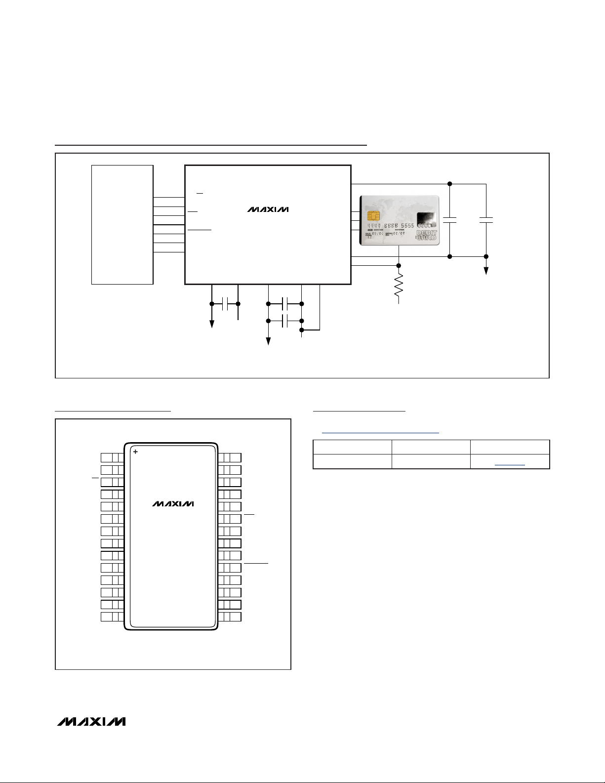
The DS8313 smart card and SIM interface IC is a lowcost, analog front-end for a smart card reader designed
for smart card applications that do not require the use
of the auxiliary card I/O contacts C4 and C8 (AUX1 and
AUX2). The DS8313 supports 5V, 3V, and 1.8V smart
cards. The absence of a charge pump reduces active
power consumption, and the DS8313 also supports an
ultra-low-power 10nA stop mode.
The DS8313 is designed to interface between a system
microcontroller and the smart card interface, providing
all power supply, protection, and level shifting required
for IC card applications.
The DS8314 is similar to the DS8313, but only uses one
analog (smart card) power supply. Therefore, the
device has reduced ability to provide power to smart
cards, but it is still sufficient for many applications,
allowing the DS8314 to drop into many TDA8024 sockets without hardware changes.
The DS8313L and DS8314L use a negative polarity-presence detect instead of the default positive-polarity detect.
Both devices are available in a 28-pin SO package.
Applications
Pay/Premium Television
Access Control
Banking Applications
POS Terminals
Debit/Credit Payment Terminals
PIN Pads
Automated Teller Machines
Telecommunications
Features
♦ Analog Interface and Level Shifting for IC Card
Communication
♦ ±8kV (min) ESD (HBM) Protection on Card Interfaces
♦ Ultra-Low Stop-Mode Current, Less Than 10nA
Typical
♦ Internal IC Card Supply-Voltage Generation
5.0V ±5%, 80mA (max)
3.0V ±8%, 65mA (max)
1.8V ±10%, 30mA (max)
♦ Automatic Card Activation and Deactivation
Controlled by Dedicated Internal Sequencer
♦ I/O Lines from Host Directly Level Shifted for
Smart Card Communication
♦ Flexible Card Clock Generation, Supporting
External Crystal Frequency Divided by 1, 2, 4, or 8
♦ High-Current, Short-Circuit and High-Temperature
Protection
♦ Low Active-Mode Current
DS8313/DS8314
Smart Card Interface
________________________________________________________________
Maxim Integrated Products
1
Ordering Information
19-4655; Rev 1; 5/09
For pricing, delivery, and ordering information, please contact Maxim Direct at 1-888-629-4642,
or visit Maxim’s website at www.maxim-ic.com.
PART TEMP RANGE PIN-PACKAGE
DS8313-RRX+ -40°C to +85°C 28 SO
DS8313L-RRX+* -40°C to +85° C 28 SO
DS8314-RRX+* -40°C to +85°C 28 SO
DS8314L-RRX+* -40°C to +85° C 28 SO
Note: Contact the factory for availability of other variants and
package options.
+
Denotes a lead(Pb)-free/RoHS-compliant package.
*
Future product—contact factory for availability.
Typical Application Circuit, Pin Configuration, and Selector
Guide appear at end of data sheet.
Note: Some revisions of this device may incorporate deviations from published specifications known as errata. Multiple revisions of any device may be
simultaneously available through various sales channels. For information about device errata, go to: www.maxim-ic.com/errata
.
DS8313/DS8314
Smart Card Interface
2 _______________________________________________________________________________________
ABSOLUTE MAXIMUM RATINGS
RECOMMENDED DC OPERATING CONDITIONS
(VDD= +3.3V, V
DDA
= +5.0V, TA= +25°C, unless otherwise noted. All specifications apply to both the DS8313 and DS8314, unless
otherwise noted in the CONDITIONS column.) (Note 1)
Stresses beyond those listed under “Absolute Maximum Ratings” may cause permanent damage to the device. These are stress ratings only, and functional
operation of the device at these or any other conditions beyond those indicated in the operational sections of the specifications is not implied. Exposure to
absolute maximum rating conditions for extended periods may affect device reliability.
Voltage Range on VDDRelative to GND ...............-0.5V to +6.5V
Voltage Range on V
DDA
Relative to GND .............-0.5V to +6.5V
Voltage Range on All Other Pins
Relative to GND......................................-0.5V to (V
DD
+ 0.5V)
Maximum Junction Temperature .....................................+125°C
Maximum Power Dissipation (T
A
= -25°C to +85°C) .......700mW
Storage Temperature Range .............................-55°C to +150°C
Soldering Temperature.........Refer to the IPC/JEDEC J-STD-020
Specification.
POWER SUPPLY
Digital Supply Voltage VDD 2.7 6.0 V
Card Voltage-Generator Supply Voltage V
Reset Voltage Thresholds
CURRENT CONSUMPTION
Active VDD Current 5V Cards
(Including 80mA Draw from 5V Card)
Active VDD Current 5V Cards (Current
Consumed by DS8313/DS8314 Only)
Active VDD Current 3V Cards
(Including 65mA Draw from 3V Card)
Active VDD Current 3V Cards (Current
Consumed by DS8313/DS8314 Only)
Active VDD Current 1.8V Cards
(Including 30mA Draw from 1.8V Card)
Active VDD Current 1.8V Cards (Current
Consumed by DS8313/DS8314 Only)
Inactive-Mode Current I
Stop-Mode Current I
PARAMETER SYMBOL CONDITIONS MIN TYP MAX UNITS
DS8313, DS8314 4.75 6.0 V
DDA
V
Threshold voltage (fall ing) 2.35 2.45 2.65 V
TH2
Hy steres is 50 100 150 mV
V
HYS2
I
DD_50V
I
DD_IC
I
DD_30V
I
DD_IC
I
DD_18V
I
DD_IC
DD
DD_STOP
ICC = 80mA, f
f
= 10MHz, V
CLK
ICC = 80mA, f
f
= 10MHz, V
CLK
ICC = 65mA, f
= 10MHz, V
f
CLK
ICC = 65mA, f
= 10MHz, V
f
CLK
ICC = 30mA, f
= 10MHz, V
f
CLK
ICC = 30mA, f
= 10MHz, V
f
CLK
Card inactive, active-high PRES,
DS8313/DS8314 not in stop mode
= 20MH z,
XTAL
DDA
= 20MHz,
XTAL
= 5.0V (Note 2)
DDA
= 20MH z,
XTAL
DDA
= 20MHz,
XTAL
= 5.0V (Note 2)
DDA
= 20MH z,
XTAL
DDA
= 20MHz,
XTAL
= 5.0V (Note 2)
DDA
= 5.0V
= 5.0V
= 5.0V
80.75 85 mA
0.75 5 mA
65.75 70 mA
0.75 5 mA
30.75 40 mA
0.75 5 mA
50 40 μA
DS8313/DS8314 in ultra-low-power
stop mode (CMDVCC, 5V/3V, and
10 μA
1_8V set to logic 1) (Note 3)
DS8313/DS8314
Smart Card Interface
_______________________________________________________________________________________ 3
RECOMMENDED DC OPERATING CONDITIONS (continued)
(VDD= +3.3V, V
DDA
= +5.0V, TA= +25°C, unless otherwise noted. All specifications apply to both the DS8313 and DS8314, unless
otherwise noted in the CONDITIONS column.) (Note 1)
PARAMETER SYMBOL CONDITIONS MIN TYP MAX UNITS
CLOCK SOURCE
Crystal Frequenc y f
XTAL1 Operating Conditions
External Capacitance for Crystal
Internal Oscillator f
External crystal (Note 1) 0 20 MHz
XTAL
f
XTAL1
V
IL_XTAL1
V
IH_XTAL1
C
XTAL1
C
XTAL2
INT
(Note 1) 0 20 MHz
Low-level input on XTAL1 -0.3
High-level input on XTAL1
,
15 pF
0.7 x
V
DD
0.3 x
V
DD
VDD +
0.3
2.2 2.7 3.4 MHz
V
SHUTDOWN TEMPERATURE
Shutdown Temperature TSD +150 °C
RST PIN
Card-Inactive Mode
Card-Active Mode
Output Low Voltage V
Output Current I
Output Low Voltage V
Output High
Voltage
V
Rise Time t
Fal l Time t
Current Limitation I
RSTIN to RS T Delay t
RST(LIMIT)
D(RSTIN-RST)
OL_RST1
I
OL_RST1
V
I
OL_RST2
I
OH_RST2
CL= 30pF (Note 1) 0.1 μs
R_RST
CL= 30pF (Note 1) 0.1 μs
F_RST
= 1mA 0 0.3 V
OL_RST
= 0 0 -1 mA
OL_RST
= 200μA 0 0.3 V
OL_RST
V
-
OH_RST
= -200μA
CC
0.5
V
-20 +20 mA
2 μs
V
CC
CLK P IN
Card-Inactive Mode
Card-Active Mode
Output Low Voltage V
Output Current I
Output Low Voltage V
Output High
Voltage
Rise Time t
Fal l Time t
Current Limitation I
Cloc k Frequency f
OL_CLK1 IOLCLK
V
OL_CLK1
I
OL_CLK2
V
OH_CLK2 IOHCLK
CL= 30pF (Notes 1, 4) 8 ns
R_CLK
CL= 30pF (Notes 1, 4) 8 ns
F_CLK
CLK(LIMIT)
-70 +70 mA
Operational 0 10 MHz
CLK
Duty Factor C
Slew Rate SR C
= 1mA 0 0.3 V
= 0 0 -1 mA
OLCLK
= 200μA 0 0.3 V
OLCLK
V
-
= -200μA
= 30pF 45 55 %
L
= 30pF (Note 1) 0.2 V/ns
L
CC
0.5
V
V
CC
VCC PIN
Card-Inactive Mode
Output Low Voltage V
Output Current I
I
CC1
VCC = 0 0 -1 mA
CC1
= 1mA 0 0.3 V
CC
DS8313/DS8314
Smart Card Interface
4 _______________________________________________________________________________________
RECOMMENDED DC OPERATING CONDITIONS (continued)
(VDD= +3.3V, V
DDA
= +5.0V, TA= +25°C, unless otherwise noted. All specifications apply to both the DS8313 and DS8314, unless
otherwise noted in the CONDITIONS column.) (Note 1)
Card-Active Mode
DATA LINES (I/O AND I/OIN)
I/O I/OIN Falling Edge Delay t
Pullup Pulse Active Time tPU (Note 1) 100 ns
Maximum Frequency f
Input Capacitance CI 10 pF
I/O PIN
Card-Inactive Mode
Card-Active Mode
PARAMETER SYMBOL CONDITIONS MIN TYP MAX UNITS
Output Low Voltage V
CC2
DS8313: I
= 4.75V (Note 1)
V
DDA
DS8313: I
DS8313: I
DS8313: I
DS8314: 65mA < I
DS8314: I
DS8314: I
DS8314: I
< 80mA,
CC(5V)
< 65mA 4.75 5 5.25
CC(5V)
< 65mA 2.78 3 3.24
CC(3V)
CC(1. 8V)
CC(5V)
CC(3V)
CC(1. 8V)
< 30mA 1.64 1.8 1.98
< 80mA 4.55 5 5.25
CC(5V)
< 65mA 4.75 5 5.25
< 65mA 2.78 3 3.24
< 30mA 1.64 1.8 1.98
4.65 5 5.25
V
5V card; current pulses of 40nC
with I < 200mA, t < 400ns,
4.6 5.4
f < 20MHz
3V card; current pulses of 24nC
with I < 200mA, t < 400ns,
2.75 3.25
f < 20MHz
1.8V card; current pulses of 12nC
with I < 200mA, t < 400ns,
1.62 1.98
f < 20MHz
Output Current I
Shutdown Current
Threshold
Slew Rate V
D(IO-I OIN)
Output Low Voltage V
Output Current I
Internal Pul lup
Resistor
Output Low Voltage V
Voltage
V
Output Rise/Fall
Time
Input Low Voltage V
Input High Voltage V
V
CC2
V
V
I
CC(SD)
CCSR
(Note 1) 120 mA
Up/down; C < 300nF (Note 5) 0.05 0.16 0.22 V/μs
(Note 1) 200 ns
1 MHz
IOMAX
I
OL_IO1
V
OL_I O1
R
To VCC 9 11 19 k
PU_I O
OL_IO2 IOL_I O
OH_IO2
t
OT
IL_IO
IH_IO
I
I
CL= 30pF (Note 1) 0.1 μs
-0.3 +0.8
1.5 V
= 0 to 5V -80
CC(5V)
= 0 to 3V -65
CC(3V)
CC(1.8V)
OL_I O
OL_IO
= 0 to 1.8V -30
= 1mA 0 0.3 V
= 0 0 -1 mA
= 1mA 0 0.3 V
= < -20μA 0.8 x VCC V
OH_IO
= < -40μA (3V/5V) 0.75 x VCC V
OH_IO
CCOutput High
CC
CC
mA
V
V
DS8313/DS8314
Smart Card Interface
_______________________________________________________________________________________ 5
RECOMMENDED DC OPERATING CONDITIONS (continued)
(VDD= +3.3V, V
DDA
= +5.0V, TA= +25°C, unless otherwise noted. All specifications apply to both the DS8313 and DS8314, unless
otherwise noted in the CONDITIONS column.) (Note 1)
PARAMETER SYMBOL CONDITIONS MIN TYP MAX UNITS
Card-Active Mode
Input Low Current I
Input High Current I
IL_IO
IH_IO
Input Rise/Fall Time tIT 1.2 μs
Current Limitation I
Current When
Pullup Active
IO(LIMIT)
I
PU
V
= 0 600 μA
IL_IO
V
= VCC 20 μA
IH_IO
CL= 30pF -15 +15 mA
CL= 80pF, VOH = 0.9 x VDD -1 mA
I/OIN PIN
Output Low Voltage VOL IOL = 1mA 0 0.3 V
Output High Voltage VOH IOH < -40μA
0.75 x
V
DD
VDD +
0.1
V
Output Rise/Fall Time tOT CL= 30pF, 10% to 90% 0.1 μs
Input Low Voltage VIL -0.3
Input High Voltage V
Input Low Current I
Input High Current I
Input Ri se/Fall Time tIT V
IH
VIL = 0 600 μA
IL_IO
VIH = VDD 10 μA
IH_IO
to VIH 1.2 μs
IL
0.7 x
V
DD
0.3 x
V
DD
VDD +
0.3
V
V
Integrated Pullup Res istor RPU Pullup to VDD 9 11 13 k
Current When Pul lup Active IPU CL= 30pF, VOH = 0.9 x VDD -1 mA
CONTROL PINS (CLKDIV1, CLKDIV2, CMDVCC, RSTIN, 5V/3V, 1_8V)
Input Low Voltage V
Input High Voltage V
Input Low Current I
Input High Current I
IH_IO
IL
IH
IL_IO
-0.3
0.7 x
V
DD
0 < VIL < VDD 5 μA
0 < VIH < VDD 5 μA
0.3 x
V
DD
VDD +
0.3
V
V
INTERRUPT OUTPUT PIN (OFF)
Output Low Voltage VOL IOL = 2mA 0 0.3 V
Output High Voltage VOH IOH = -15μA
0.75 x
V
DD
V
Integrated Pullup Res istor RPU Pullup to VDD 16 24 32 k
PRES PIN
Input Low Voltage V
Input High Voltage V
IL_PRES
IH_PRES
0.7 x
V
DD
0.3 x
V
DD
V
V
DS8313/DS8314
Smart Card Interface
6 _______________________________________________________________________________________
RECOMMENDED DC OPERATING CONDITIONS (continued)
(VDD= +3.3V, V
DDA
= +5.0V, TA= +25°C, unless otherwise noted. All specifications apply to both the DS8313 and DS8314, unless
otherwise noted in the CONDITIONS column.) (Note 1)
Note 1: Operation guaranteed at -40°C and +85°C but not tested.
Note 2: I
DD_IC
measures the amount of current used by the DS8313 to provide the smart card current minus the load.
Note 3: Stop mode is enabled by setting CMDVCC, 5V/3V, and 1_8V to a logic-high.
Note 4: Parameters are guaranteed to meet all ISO 7816, GSM11-11, and EMV 2000 requirements. For the 1.8V card, the maximum
rise and fall time is 10ns.
Note 5: Parameter is guaranteed to meet all ISO 7816, GSM11-11, and EMV 2000 requirements. For the 1.8V card, the minimum
slew rate is 0.05V/µs and the maximum slew rate is 0.5V/µs.
Input Low Current I
Input High Current I
TIMING
Activation Time t
Deactivation Time t
CLK to Card Start
Time
PRES Debounce Time t
PARAMETER SYMBOL CONDITIONS MIN TYP MAX UNITS
IL_PRES
IH_PRES
ACT
DEACT
Window Start t3 50 130
Window End t
5
DEB OUNCE
V
V
50 220 μs
50 80 100 μs
140 220
5 8 11 ms
= 0 5 μA
IL_PR ES
= VDD 10 μA
IH_PRES
μs
DS8313/DS8314
Smart Card Interface
_______________________________________________________________________________________ 7
Pin Description
PIN NAME FUNCTION
1, 2
3 5V/3V
4 1_8V
5, 7, 8, 9,
12, 13, 27,
28
6, 18
10 PRES
11 I/O Smart Card Data-Line Output. Card data communication line, contact C7.
14 CGND Smart Card Ground
15 CLK Smart Card Clock. Card clock, contact C3.
16 RST Smart Card Reset. Card reset output from contact C2.
17 V
19 CMDVCC Activation Sequence In itiate. Acti ve-low input from host.
20 RSTIN Card Re set Input. Re set input from the host.
21 VDD Supply Voltage
22 GND Digital Ground
23 OFF
24, 25
26 I/OIN I/O Input. Host-to- interface chip data I/O line.
CLKDIV1,
CLKDIV2
N.C. No Connection/Don’t Care. These pins are not bonded out.
V
DDA
(N.C.)
CC
XTAL1,
XTAL2
Cloc k D ivider. Determine s the div ided-down input clock frequenc y (presented at XTAL1 or from a
crystal at XTAL1 and XTAL2) on the CLK output pin. Div ider s of 1, 2, 4, and 8 are available.
5V/3V Selection Pin. A llow s selection of 5V or 3V for communication with an IC card. Logic-high
selects 5V operation; log ic-low selects 3V operation. The 1_8V pin overrides the setting on thi s pin if
active. See Table 3 for a complete description of choosing card voltages.
1.8V Operation Select ion. Active-high selection for 1.8V smart card communication. An active-h igh
signal on this pin overrides any setting on the 5V/3V pin.
Analog (Smart Card) Supply. Connect to 5V power supply. Pin 18 is N.C. for the DS8314.
Card Presence Ind icator. Acti ve-high card presence input from the DS8313 to the microcontroller.
When the presence indicator becomes active, a debounce timeout begins. After 8ms (typ), the OFF
signal becomes active. A trim optim defines whether or not the part provides active-low presence
detection.
Smart Card Supply Voltage. Decouple to CGND (card ground) with 2 x 100nF or 100 + 220nF
capacitors (ESR < 100m).
Status Output. Acti ve-low interrupt output to the host. Include s a 24k integrated pullup resistor to
.
V
DD
Crystal/Clock Input. Connect an input from an external clock to XTAL1 or connect a crystal across
XTAL1 and XTAL2. For the low idle-mode current variant, an external clock must be driven on
XTAL1.

DS8313/DS8314
Smart Card Interface
8 _______________________________________________________________________________________
Detailed Description
The DS8313 is an analog front-end for communicating
with 1.8V, 3V, and 5V smart cards. It is a dual inputvoltage device, requiring one supply to match that of a
host microcontroller and a separate +5V supply for
generating correct smart card supply voltages. The
DS8313 translates all communication lines to the correct voltage level and provides power for smart card
operation. It is a low-power device, consuming very lit-
tle current in active-mode operation (during a smart
card communication session), and is suitable for use in
battery-powered devices such as laptops and PDAs,
consuming only 10nA in stop mode. The DS8313 is
designed for applications that do not require communication using the C4 and C8 card contacts (AUX1 and
AUX2). It is suitable for SIM/SAM interfacing, as well as
for applications where only the I/O line is used to communicate with a smart card.
The DS8314 is nearly identical to the DS8313, but only
uses one V
DDA
input; therefore, it has reduced capacity to deliver current to 5V smart cards. However, the
DS8314 can drop into many existing TDA8024 applications with minimal or no hardware changes. See Figure
1 for a functional diagram.
Power Supply
The DS8313/DS8314 are dual-supply devices. The supply pins for the devices are VDD, GND, and V
DDA
. V
DD
should be in the 2.7V to 6.0V range, and is the supply
for signals that interface with the host controller. It
should, therefore, be the same supply as used by the
host controller. All smart card contacts remain inactive
during power-on or power-off. The internal circuits are
kept in the reset state until VDDreaches V
TH2
+ V
HYS2
and for the duration of the internal power-on reset
pulse, tW. A deactivation sequence is executed when
VDDfalls below V
TH2
.
An internal regulator generates the 1.8V, 3V, or 5V card
supply voltage (VCC). The regulator should be supplied
separately by V
DDA
. V
DDA
should be connected to a
minimum 4.75V supply to provide the correct supply
voltage for 5V smart cards.
Figure 1. Functional Diagram
Figure 2. Voltage Supervisor Behavior
V
GND
DD
POWER-SUPPLY
SUPERVISOR
CARD VOLTAGE
GENERATOR
XTAL1
XTAL2
CLKDIV1
CLKDIV2
1_8V
5V/3V
CMDVCC
RSTIN
PRES
OFF
I/OIN
*USED ONLY ON THE DS8313.
GENERATION
CLOCK
TEMPERATURE
MONITOR
CONTROL
SEQUENCER
I/O TRANSCEIVER
DS8313
DS8314
V
DDA
V
DDA
V
CC
CGND
RST
CLK
I/O
*
V
DD
(INTERNAL SIGNAL)
ALARM
t
W
POWER ON
t
W
SUPPLY DROPOUT
+ V
V
TH2
V
TH2
POWER OFF
HYS2

Voltage Supervisor
The voltage supervisor monitors the VDDsupply. A
220µs reset pulse (tW) is used internally to keep the
device inactive during power-on or power-off of the
V
DD
supply. See Figure 2.
The DS8313/DS8314 card interface remains inactive
regardless of the levels on the command lines until
duration tWafter VDDhas reached a level higher than
V
TH2
+ V
HYS2
. When VDDfalls below V
TH2
, the
DS8313/DS8314 execute a card deactivation sequence
if their card interface is active.
Clock Circuitry
The card clock signal (CLK) is derived from a clock signal input to XTAL1 or from a crystal operating at up to
20MHz connected between XTAL1 and XTAL2. The
output clock frequency of CLK is selectable through
inputs CLKDIV1 and CLKDIV2. The CLK signal frequency can be f
XTAL
, f
XTAL
/2, f
XTAL
/4, or f
XTAL
/8. See Table
1 for the frequency generated on the CLK signal given
the inputs to CLKDIV1 and CLKDIV2.
Note that CLKDIV1 and CLKDIV2 must not be changed
simultaneously; a delay of 10ns minimum between
changes is needed. The minimum duration of any state
of CLK is eight periods of XTAL1.
The frequency change is synchronous: during a transition
of the clock divider, no pulse is shorter than 45% of the
smallest period, and the first and last clock pulses about
the instant of change have the correct width. When
changing the frequency dynamically, the change is effective for only eight periods of XTAL1 after the command.
The f
XTAL
duty factor depends on the input signal on
XTAL1. To reach a 45% to 55% duty factor on CLK,
XTAL1 should have a 48% to 52% duty factor with transition times less than 5% of the period.
With a crystal, the duty factor on CLK can be 45% to
55% depending on the circuit layout and on the crystal
characteristics and frequency. In other cases, the duty
factor on CLK is guaranteed between 45% and 55% of
the clock period.
I/O Transceivers
I/O and I/OIN are pulled high with an 11kΩ resistor (I/O
to VCCand I/OIN to VDD) in the inactive state. The first
side of the transceiver to receive a falling edge
becomes the master. When a falling edge is detected
(and the master is decided), the detection of falling
edges on the line of the other side is disabled; that side
then becomes a slave. After a time delay t
D(EDGE)
, an n
transistor on the slave side is turned on, thus transmitting the logic 0 present on the master side.
When the master side asserts a logic 1, a p transistor
on the slave side is activated during the time delay t
PU
and then both sides return to their inactive (pulled up)
states. This active pullup provides fast low-to-high transitions. After the duration of t
PU
, the output voltage
depends only on the internal pullup resistor and the
load current. Current to and from the card I/O lines is
limited internally to 15mA. The maximum frequency on
these lines is 1MHz.
Inactive Mode
The DS8313/DS8314 power up with the card interface
in the inactive mode. Minimal circuitry is active while
waiting for the host to initiate a smart card session.
• All card contacts are inactive (approximately 200Ω
to GND).
• The I/OIN pin in the high-impedance state (11kΩ
pullup resistor to VDD).
• Voltage generators are stopped.
• XTAL oscillator is running (if included in the device).
• Voltage supervisor is active.
• The internal oscillator is running at its low frequency.
Activation Sequence
After power-on and the reset delay, the host microcontroller can monitor card presence with signals OFF and
CMDVCC, as shown in Table 2.
DS8313/DS8314
Smart Card Interface
_______________________________________________________________________________________ 9
Table 1. Clock Frequency Selection
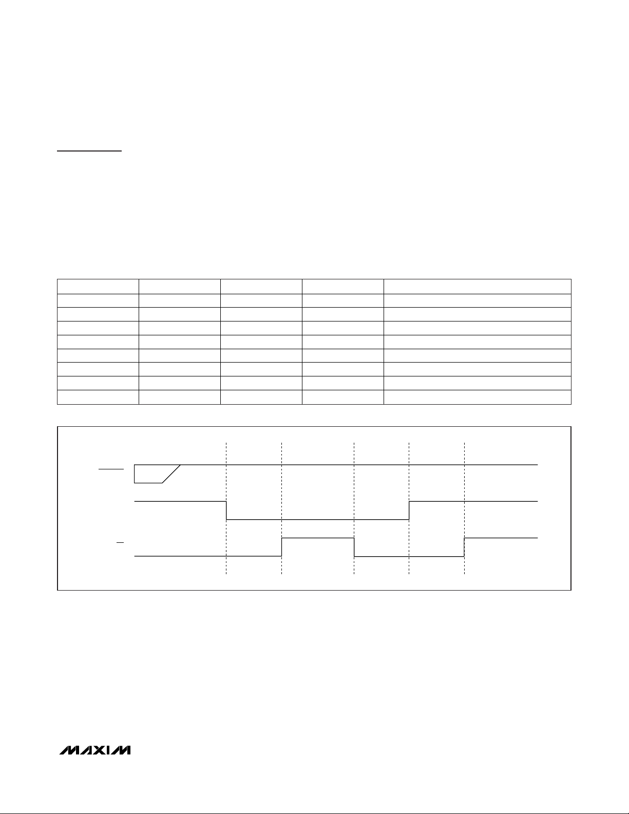
Table 2. Card Presence Indication
CLKDIV1 CLKDIV2 f
0 0 f
0 1 f
1 1 f
1 0 f
CLK
XTAL
XTAL
XTAL
XTAL
OFF CMDVCC STATUS
/8
/4
/2
High High Card present.
Low High Card not present.

DS8313/DS8314
If the card is in the reader (if PRES is active), the host
microcontroller can begin an activation sequence (start
a card session) by pulling CMDVCC low. The following
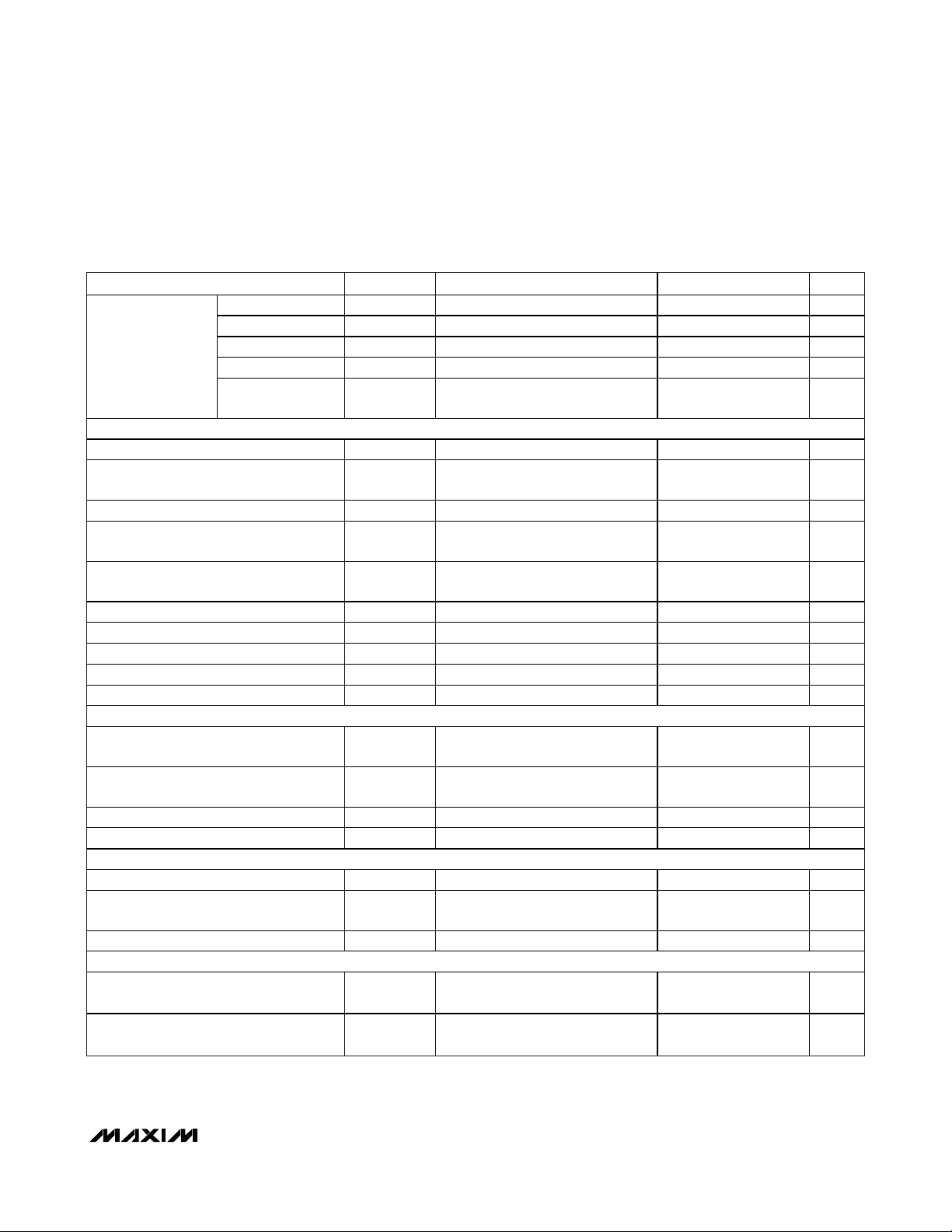
events form an activation sequence (Figure 3):
1) CMDVCC is pulled low.
2) The internal oscillator changes to high frequency (t0).
3) The voltage generator is started (between t0and t1).
4) V
CC
rises from 0 to 5V, 3V, or 1.8V with a con-
trolled slope (t
2
= t1+ 1.5 × T). T is 64 times the
internal oscillator period (approximately 25µs).
5) I/O pin is enabled (t
3
= t1+ 4T) (they were previ-
ously pulled low).
6) The CLK signal is applied to the C3 contact (t
4
).
7) RST is enabled (t5= t1+ 7T).
To apply the clock to the card interface:
1) Set RSTIN high.
2) Set CMDVCC low.
3) Set RSTIN low between t
3
and t5; CLK will now start.
4) RST stays low until t5, then RST becomes the copy
of RSTIN.
5) RSTIN has no further effect on CLK after t
5
.
If the applied clock is not needed, set CMDVCC low
with RSTIN low. In this case, CLK starts at t3(minimum
200ns after the transition on I/O, see Figure 4); after t5,
RSTIN can be set high to obtain an answer to request
(ATR) from an inserted smart card. Do not perform activation with RSTIN held permanently high.
Active Mode
When the activation sequence is completed, the card
interface is in active mode. The host microcontroller
and the smart card exchange data on the I/O lines.
Smart Card Interface
10 ______________________________________________________________________________________
Figure 3. Activation Sequence Using RSTIN and CMDVCC
CMDVCC
V
CC
I/O
CLK
RSTIN
RST
I/OIN
t
0t1
t
2
t
3
t
t5 = t
4
ACT
ATR
DS8313/DS8314
Smart Card Interface
______________________________________________________________________________________ 11
CMDVCC
Figure 4. Activation Sequence at t
3
Figure 5. Deactivation Sequence
V
CC
I/O
CLK
RSTIN
RST
I/OIN
CMDVCC
RST
t
0t1
ATR
200ns
t
2
t3t
4
t5 = t
ACT
CLK
I/O
V
CC
t
10
t
12
t
13
t
DE
t
14
t
15

DS8313/DS8314
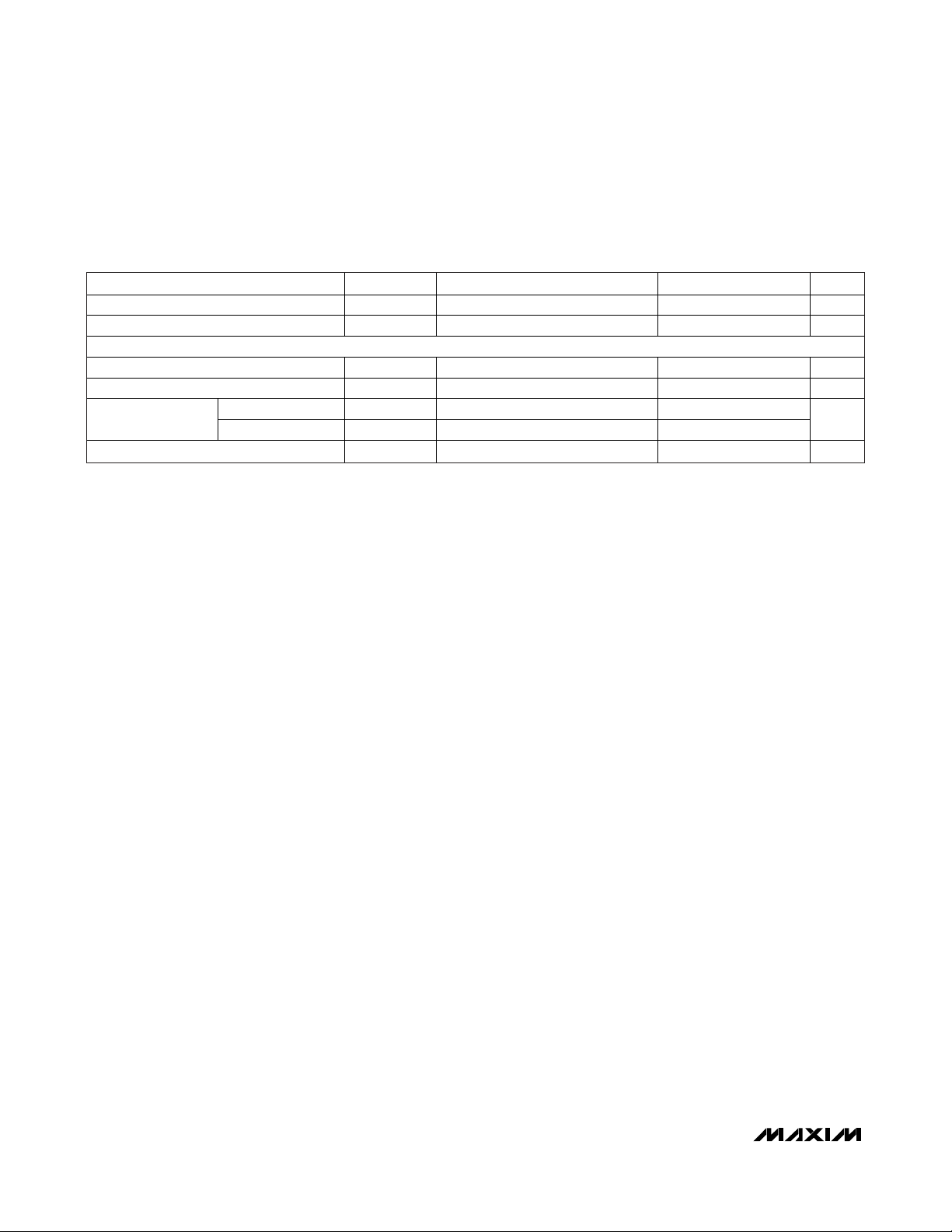
Deactivation Sequence
When a session is completed, the host microcontroller
sets the CMDVCC line high to execute an automatic
deactivation sequence and returns the card interface to
the inactive mode (Figure 5).
1) RST goes low (t10).
2) CLK is held low (t12= t10+ 0.5 × T) where T is 64
times the period of the internal oscillator (approximately 25µs).
3) I/O pin is pulled low (t13= t10+ T).
4) V
CC
starts to fall (t14= t10+ 1.5 × T).
5) When V
CC
reaches its inactive state, the deactiva-
tion sequence is complete (at tDE).
6) All card contacts become low impedance to GND;
I/OIN remains at V
DD
(pulled up through an 11kΩ
resistor).
7) The internal oscillator returns to its lower frequency.
V
CC
Generator
The VCCgenerator has a capacity to supply up to
80mA continuously at 5V, 65mA at 3V, and 30mA at
1.8V. An internal overload detector triggers at approximately 120mA. Current samples to the detector are filtered. This allows spurious current pulses (with a
duration of a few µs) up to 200mA to be drawn without
causing deactivation. The average current must stay
below the specified maximum current value. To maintain V
CC
voltage accuracy, a 100nF capacitor (with an
ESR < 100mΩ) should be connected to CGND and
placed near the V
CC
pin, and a 100nF or 220nF capacitor (220nF is the best choice) with the same ESR should
be connected to CGND and placed near the smart
card reader’s C1 contact.
Fault Detection
The following fault conditions are monitored:
• Short-circuit or high current on V
CC
• Removal of a card during a transaction
•VDDdropping
• Card voltage generator operating out of the specified values (V
DDA
too low or current consumption
too high)
• Overheating
There are two different cases (Figure 6):
• CMDVCC High Outside a Card Session. Output
OFF is low if a card is not in the card reader and
high if a card is in the reader. The V
DD
supply is
monitored—a decrease in input voltage generates
an internal power-on reset pulse but does not
affect the OFF signal. Short-circuit and temperature detection is disabled because the card is not
powered up.
• CMDVCC Low Within a Card Session. Output
OFF goes low when a fault condition is detected,
and an emergency deactivation is performed automatically (Figure 7). When the system controller
resets CMDVCC to high, it may sense the OFF
level again after completing the deactivation
sequence. This distinguishes between a card
extraction and a hardware problem (OFF goes high
again if a card is present). Depending on the connector’s card-present switch (normally closed or
normally open) and the mechanical characteristics
of the switch, bouncing can occur on the PRES signals at card insertion or withdrawal.
The DS8313/DS8314 have a debounce feature with an
8ms typical duration (Figure 6). When a card is inserted, output OFF goes high after the debounce time
delay. When the card is extracted, an automatic deactivation sequence of the card is performed on the first
true/false transition on PRES and output OFF goes low.
Smart Card Interface
12 ______________________________________________________________________________________

DS8313/DS8314
Smart Card Interface
______________________________________________________________________________________ 13
PRES
Figure 6. Behavior of PRES, OFF, CMDVCC, and V
CC
Figure 7. Emergency Deactivation Sequence (Card Extraction)
OFF
CMDVCC
V
DEBOUNCE DEBOUNCE
CC
DEACTIVATION CAUSED
BY CARD WITHDRAWAL
OFF
PRES
RST
CLK
I/O
V
CC
DEACTIVATION CAUSED
BY SHORT CIRCUIT
t
10
t
12
t
13
t
DE
t
14
t
15

DS8313/DS8314
Stop Mode (Low-Power Mode)
A low-power state, stop mode, can be entered by forcing the CMDVCC, 5V/3V, and 1_8V input pins to a
logic-high state. Stop mode can only be entered when
the smart card interface is inactive. In stop mode, all
internal analog circuits are disabled. The OFF pin follows the status of the PRES pin. To exit stop mode,
change the state of one or more of the three control
pins to a logic-low. An internal 220µs (typ) power-up
delay and the 8ms PRES debounce delay are in effect
and OFF is asserted to allow the internal circuitry to stabilize. This prevents smart card access from occurring
after leaving the stop mode. Figure 8 shows the control
sequence for entering and exiting stop mode. Note that
an in-progress deactivation sequence always finishes
before the DS8313/DS8314 enter low-power stop
mode.
Smart Card Interface
14 ______________________________________________________________________________________
Figure 8. Stop-Mode Sequence
DEACTIVATE INTERFACE
CMDVCC
1_8V
5V/3V
STOP MODE
ACTIVATE
STOP MODE
DEACTIVATE
STOP MODE
220μs DELAY
8ms DEBOUNCE
OFF ASSERTED TO
OFF
OFF FOLLOWS
PRES IN STOP MODE
PRES
V
CC
WAIT FOR DELAY
Smart Card Power Select
The DS8313/DS8314 support three smart card V
CC
voltages: 1.8V, 3V, and 5V. The power select is controlled by the 1_8V and 5V/3V signals as shown in
Table 3. The 1_8V signal has priority over 5V/3V. When
1_8V is asserted high, 1.8V is applied to VCCwhen the
smart card is active. When 1_8V is deasserted, 5V/3V
dictates VCCpower range. VCCis 5V if 5V/3V is asserted to a logic-high state, and V
CC
is 3V if 5V/3V is pulled
to a logic-low state. Care must be exercised when
switching from one V
CC
power selection to the other. If
both 1_8V and 5V/3V are high with CMDVCC high at
the same time, the DS8313/DS8314 enter stop mode.
To avoid accidental entry into stop mode, the state of
1_8V and 5V/3V must not be changed simultaneously.
A minimum delay of 100ns should be observed
between changing the states of 1_8V and 5V/3V. See
Figure 9 for the recommended sequence of changing
the VCCrange.
DS8313/DS8314
Smart Card Interface
______________________________________________________________________________________ 15
Figure 9. Smart Card Power Select
Table 3. VCCSelect and Operation Mode
1_8V 5V/3V CMDVCC VCC SELECT (V) CARD INTERFACE STATUS
0 0 0 3 Activated
0 0 1 3 Inactivated
0 1 0 5 Activated
0 1 1 5 Inactivated
1 0 0 1.8 Activated
1 0 1 1.8 Inactivated
1 1 0 1.8 Reserved (Activated)
1 1 1 1.8 Not Applicable—Stop Mode
VCC SELECT STOP MODE1.8V 1.8V3V 3V5V
CMDVCC
1_8V
5V/3V
DS8313/DS8314
Smart Card Interface
16 ______________________________________________________________________________________
Applications Information
Performance can be affected by the layout of the application. For example, an additional cross-capacitance of
1pF between card reader contacts C2 (RST) and C3
(CLK) or C2 (RST) and C7 (I/O) can cause contact C2
to be polluted with high-frequency noise from C3 (or
C7). In this case, include a 100pF capacitor between
contacts C2 and CGND.
Application recommendations include the following:
• Ensure there is ample ground area around the
DS8313/DS8314 and the connector; place the
DS8313/DS8314 very near to the connector; decouple the VDDand V
DDA
lines separately. These lines
are best positioned under the connector.
• The device and the host microcontroller must use
the same V
DD
supply. Pins CLKDIV1, CLKDIV2,
RSTIN, PRES, I/OIN, 5V/3V, 1_8V, CMDVCC, and
OFF are referenced to VDD; if pin XTAL1 is to be
driven by an external clock, also reference this pin
to V
DD
.
• Trace C3 (CLK) should be placed as far as possible from the other traces.
• The trace connecting CGND to C5 (GND) should
be straight (the two capacitors on C1 (VCC) should
be connected to this ground trace).
• Avoid ground loops between CGND and GND.
• Decouple V
DDA
and VDDseparately. If two supplies are the same in the application, they should
be connected in a star on the main trace
With all these layout precautions, noise should be kept to
an acceptable level and jitter on C3 (CLK) should be less
than 100ps. Reference layouts are available on request.
Technical Support
For technical support, go to https://support.maxim-
ic.com/micro.
Selector Guide
Note: Contact the factory for availability of other variants and package options.
+
Denotes a lead(Pb)-free/RoHS-compliant package.
*
Future product—contact factory for availability.
PART
DS8313-RRX+ Yes Yes Positi ve 2 28 SO
DS8313L-RRX+* Yes Yes Negative 2 28 SO
DS8314-RRX+* Yes Yes Positive 1 28 SO
DS8314L-RRX+* Yes Yes Negative 1 28 SO
LOW STOP-MODE
POWER
LOW ACTIVE-
MODE POWER
PRES POLARITY V
INPUTS PIN-PACKAGE
DDA
DS8313/DS8314
Smart Card Interface
______________________________________________________________________________________ 17
PACKAGE TYPE PACKAGE CODE DOCUMENT NO.
28 SO W28+1
21-0042
1_8V
28
27
26
25
24
23
22
N.C.
N.C.
I/OIN
XTAL2
TOP VIEW
XTAL1
OFF
GND
21 V
DD
20 RSTIN
19 CMDVCC
18 V
DDA
(N.C.)
17 V
CC
16 RST
15 CLK
5V/3V
CLKDIV2
CLKDIV1
() INDICATES DS8314 ONLY.
N.C.
V
DDA
N.C.
N.C.
PRES
I/O
N.C.
N.C.
4
1
2
3
5
6
7
8
9
10
11
12
13
14CGND
N.C.
SO
DS8313
DS8314
Pin Configuration
+3.3V
100kΩ
*PLACE A 100nF CAPACITOR CLOSE TO DS8313 AND PLACE A 220nF CAPACITOR CLOSE TO CARD CONTACT.
GPIO
μC
...
...
GPIO
ISO_DATA
100nF* 220nF*
100nF
+3.3V
I/OIN
CMDVCC
...
RSTIN
ISO_CLOCK
CLKIN
OFF
1_8V
5V/3V
PRES
CGND
I/O
CLK
RST
V
CC
GND V
DD
+10μF
GND V
DDAVDDA
100nF
+5.0V
DS8313
Typical Application Circuit
Package Information
For the latest package outline information and land patterns, go
to www.maxim-ic.com/packages
.
DS8313/DS8314
Smart Card Interface
Maxim cannot assume responsibility for use of any circuitry other than circuitry entirely embodied in a Maxim product. No circuit patent licenses are
implied. Maxim reserves the right to change the circuitry and specifications without notice at any time.
18
____________________Maxim Integrated Products, 120 San Gabriel Drive, Sunnyvale, CA 94086 408-737-7600
© 2009 Maxim Integrated Products Maxim is a registered trademark of Maxim Integrated Products, Inc.
Revision History
REVISION
NUMBER
0 1/09 Initial release. —
1 5/09
REVISION
DATE
Removed the TSSOP package variant from the General De scription, Ordering
Informat ion, Selector Guide, and Package Information sections.
Changed “(IEC)” in the Features section to “(HBM)” for the “±8 kV (min) ESD (HBM)
Protection on Card Interfaces” bullet.
DESCRIPTION
PAGES
CHANGED
1, 16, 17
1
 Loading...