

Page 1
DS8007
Multiprotocol Dual Smart Card Interface
________________________________________________________________
Maxim Integrated Products
1
For pricing, delivery, and ordering information, please contact Maxim Direct at 1-888-629-4642,
or visit Maxim’s website at www.maxim-ic.com.
General Description
The DS8007 multiprotocol dual smart card interface is a
low-cost, dual smart card reader interface supporting
all ISO 7816, EMV
®
, and GSM11-11 requirements.
Through its 8-bit parallel bus and dedicated address
selects (AD3–AD0), the DS8007 can easily and directly
connect to the nonmultiplexed byte-wide bus of a
Maxim secure microcontroller. Optionally, the parallel
bus can be multiplexed to allow direct access to the
multiplexed bus of an 80C51-compatible microcontroller through MOVX memory addressing.
One integrated ISO 7816 UART is multiplexed among
the interfaces to allow high-speed automatic smart card
processing with each card-possessing, independent,
variable, baud-rate capability. The card interface is controlled by internal sequencers that support automatic
activation and deactivation sequencing, handling all
actions required for T = 0, T = 1, and synchronous protocols. Emergency deactivation is also supported in
case of supply dropout. A third card is supported
through the auxiliary I/O. The same set of I/O can optionally be used as additional serial interface for the UART.
The DS8007 provides all electrical signals necessary to
interface with two smart cards. The integrated voltage
converter ensures full cross-compatibility between 1.8V/
3V/5V cards and a 1.8V/3V/5V environment, and allows
operation within a 2.7V to 6V supply voltage range.
Applications
Banking Applications (Point-of-Sale Terminals,
Debit/Credit Payment Terminals, PIN Pads,
Automated Teller Machines)
Telecommunications
Pay Television
Access Control
Features
♦ Integrated ISO 7816 UART Provides Complete
Interface/Control for Two Separate Smart Card
Devices
♦ 8kV (min) ESD Protection on Card Interfaces
♦ Internal IC Card Supply Voltage Generation
5.0V ±5%, 65mA (max)
3.0V ±8%, 50mA (max)
1.8V ±10%, 30mA (max)
♦ Automatic Card Activation, Deactivation, and Data
Communication Controlled by Dedicated Internal
Sequencer
♦ Host Interface Through an 8-Bit Parallel Bus (User-
Selectable Multiplexed or Nonmultiplexed Modes)
♦ Chip Select and Three-State Bus Allow Multiple
Devices (Card Readers and Memories) on Bus
♦ 8-Character Receive FIFO with Optional
Programmable Depth/Threshold
♦ I/O Interface Pin to External ISO 7816 UART for
Auxiliary Interface
♦ Separate Card Clock Generation (Up to 10MHz)
with 2x Frequency Doubling
♦ Selectable Card Clock Stop High, Stop Low, or
Internally Generated 1.25MHz (for Card PowerDown)
♦ EMV-Certified Reference Design and Evaluation
Kit Available (DS8007-KIT)
19-5972; Rev 3; 7/11
EVALUATION KIT
AVAILABLE
Ordering Information
Typical Operating Circuit appears at end of data sheet.
+
Denotes a lead(Pb)-free/RoHS-compliant package.
EMV is a registered trademark of EMVCo LLC.
MAXQ is a registered trademark of Maxim Integrated Products, Inc.
Note: Some revisions of this device may incorporate deviations from published specifications known as errata. Multiple
revisions of any device may be simultaneously available
through various sales channels. For information about device
errata, go to: www.maxim-ic.com/errata
.
RD
D7
D6
D5
D4
D3
D2
D1
D0
V
DD
CPA2
AGND
RSTOUT
I/OAUX
I/OA
C8A
PRESA
C4A
GNDA
CLKA
V
CCA
RSTA
I/OB
C8B
1
2
3
4
5
6
7
8
9
10
11
12
1314151617181920212223
24
4847464544434241403938
37
36
35
34
33
32
31
30
29
28
27
26
25
PRESB
C4B
GNDB
CLKB
V
CCB
RSTB
GND
V
UP
CPA1
CPB1
V
DDA
CPB2
DELAY
XTAL1
XTAL2
AD0
AD1
AD2
AD3
INTAUX
INT
ALECSWR
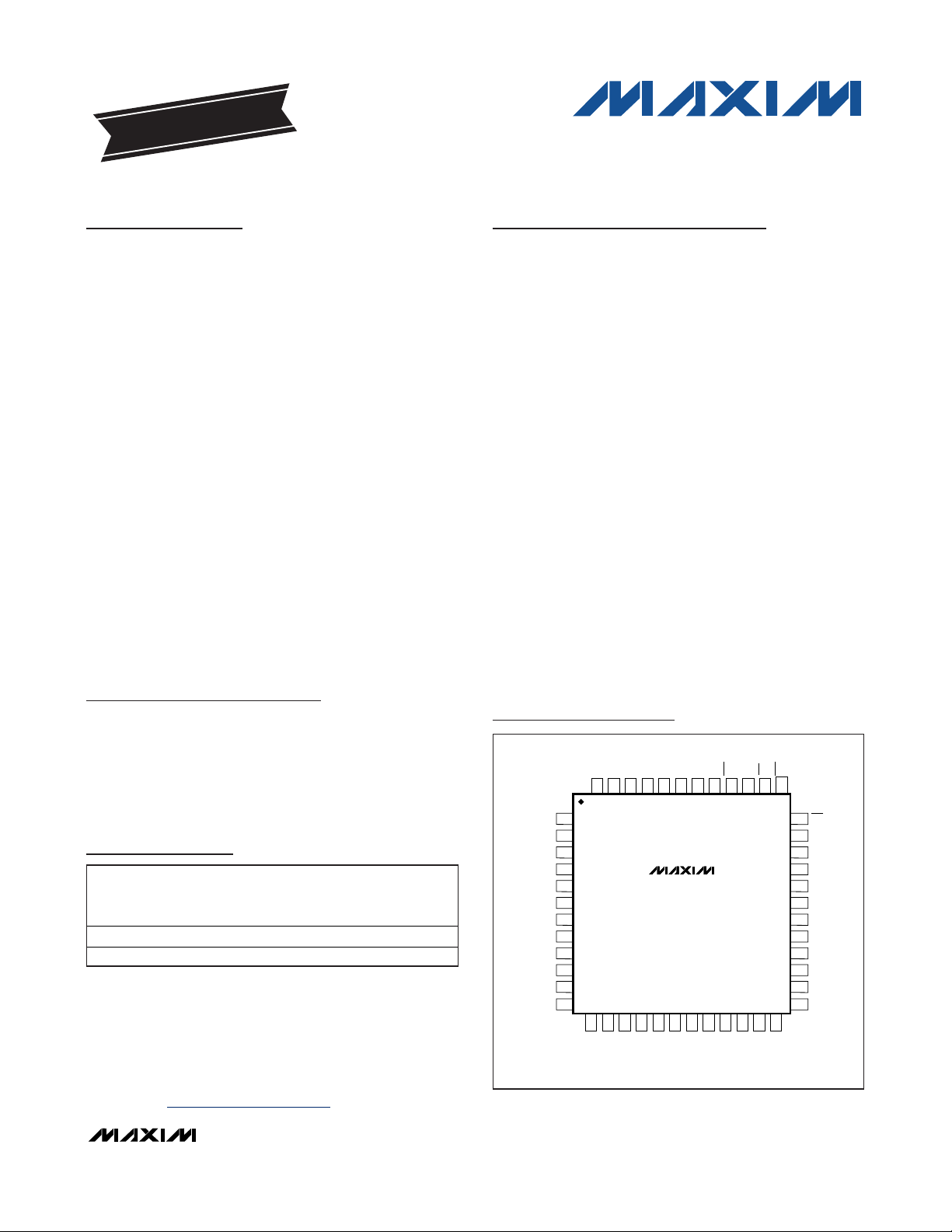
LQFP
DS8007
Pin Configuration
SMART
PART TEMP RANGE
DS8007-ENG -40°C to +85°C
DS8007-ENG+ -40°C to +85°C
SUPPORTED
2 + auxiliary
2 + auxiliary
CARDS
PINPACKAGE
48 LQFP
48 LQFP
Page 2
DS8007
Multiprotocol Dual Smart Card Interface
2 _______________________________________________________________________________________
ABSOLUTE MAXIMUM RATINGS
ELECTRICAL CHARACTERISTICS
(VDD= +3.3V, V
DDA
= +3.3V, TA= +25°C, unless otherwise noted.) (Note 1)
Stresses beyond those listed under “Absolute Maximum Ratings” may cause permanent damage to the device. These are stress ratings only, and functional
operation of the device at these or any other conditions beyond those indicated in the operational sections of the specifications is not implied. Exposure to
absolute maximum rating conditions for extended periods may affect device reliability.
Voltage Range on VDDRelative to Ground ...........-0.5V to +6.5V
Voltage Range on V
DDA
Relative to Ground .........-0.5V to +6.5V
Voltage Range on Any Pin Relative to Ground
Pins CPA1, CPA2, CPB1, CPB2, and V
UP
.........-0.5V to +7.5V
All Other Pins...........................................-0.5V to (V
DD
+ 0.5V)
Maximum Junction Temperature .....................................+150°C
Continuous Power Dissipation (T
A
= +70°C)
LQFP Multilayer Board
(derate 22mW/°C above +70°C).................................1782mW
Operating Temperature Range ...........................-40°C to +85°C
Storage Temperature Range .............................-65°C to +150°C
Lead Temperature (soldering, 10s) .................................+300°C
Soldering Temperature (reflow) .......................................+260°C
PARAMETER S YMBOL CONDITIONS MIN TYP MAX UNITS
Digital Supply Voltage VDD 2.7 6.0 V
Step-Up Converter Supply
Voltage
Power-Down
V
Current
DD
Sleep Mode VDD Current
(Cards Active)
Active VDD Current
5V Cards
Active VDD Current
3V Cards
Power-Fail Reset Voltage
Delay Pin
RSTOUT PIN
Output High Voltage V
Output Low Voltage V
Leakage Current IL VOL = 0V, VOH = 5V -10 +10 μA
V
VDD 6.0 V
DDA
Cards Inactive f
Cards Acti ve
I
PD
I
STOP
f
= 0MHz 0.9
XTAL
f
= 0MHz, f
XTAL
= 0MH z, V
CLK
= 0MH z, V
CLK
= 5V 24 mA
CCx
= 5V 2.2
CCx
3x VDD step-up:
I
DD
I
CCA
f
XTAL
+ I
= 80mA, VDD = 2.7V,
CCB
= 20MH z, f
CLK
= 10MHz
2x VDD step-up:
I
+ I
Reset
Threshold
CCA
f
CLK
No step-up:
I
CCA
f
CLK
Threshold voltage (fall ing) 2.1 2.5 V
Hysteresis 50 170 mV
1.25
V
V
V
I
DD
RST
HYS
DRST
= 80mA, f
CCB
= 10MHz, VDD = 2.7V
+ I
= 80mA, f
CCB
= 10MHz, VDD = 5V
= 20MHz,
XTAL
= 20MHz,
XTAL
Output Voltage VDO
V
= 0V -2 μA
Output Current I
Output
Capacitance
OHRSTO
OLRSTO
DO
C
DO
DELAY
V
= VDD +2 mA
DELAY
1 nF
IOH = -1mA
IOL = 2mA -0.3 +0.4 V
mA
325 mA
225
mA
120
V
V
+
DD
0.3
0.8 x
V
DD
VDD +
0.3
V
Page 3
DS8007
Multiprotocol Dual Smart Card Interface
_______________________________________________________________________________________ 3
ELECTRICAL CHARACTERISTICS (continued)
(VDD= +3.3V, V
DDA
= +3.3V, TA= +25°C, unless otherwise noted.) (Note 1)
PARAMETER S YMBOL CONDITIONS MIN TYP MAX UNITS
Alarm Pulse Width tW C
External Cloc k Frequency f
Internal Oscillator f
Voltage on VUP Pin V
Voltage Detection of V
3x Step-Up
Shutdown Temperature TSD +150 °C
Card
Inactive
Mode
RSTx
Pins
Card
Active
Mode
Card
Inactive
Mode
CLKx
Card
Pins
Active
Mode
Cloc k Frequency f
Duty Factor C
= 22nF 10 ms
DELAY
External cry stal 4 20
External oscillator 0 20
1.6 2.5 3.7 MHz
3x step-up 5.7
2x step-up 4.1
3.35 3.50 3.60 V
I
V
I
I
= 1mA 0 0.3 V
OLRST
= 0V 0 -1 mA
OLRST
= +200μA 0 0.3
OLRST
= -200μA
OHRST
CL = 30pF 0.1
CL = 30pF 0.1
-25
-25 +25
I
V
I
I
= 1mA 0 0.3 V
OLCLK
= 0V 0 -1 mA
OLCLK
= +200μA 0 0.3
OLCLK
= -200μA
OHCLK
CL = 30pF (Note 2) 8
CL = 30pF (Note 2) 8
-70 +70 mA
Idle configuration (1MHz) 1 1.85
Operational 0 10
= 30pF 45 55 %
L
for 2x,
DDA
Output Low
Voltage
Output Current I
Output Low
Voltage
Output High
Voltage
V
Rise Time t
Fal l Time t
Shutdown
Current
Current
Limitation
I
RST(LIMIT)
Output Low
Voltage
Output Current I
Output Low
Voltage
Output High
Voltage
Rise Time t
Fal l Time t
Current
Limitation
I
CLK(LIMIT)
XTAL
INT
UP
V
DET
V
OLRST
OLRST
V
OLRSTL
OHRSTH
RRST
FRST
I
RST(SD)
V
OLCLK
OLCLK
V
OLCLK
V
OHCLK
RCLK
FCLK
CLK
MHz
V
V
V
–
CCx
0.5
V
CCx
μs
mA
V
V
–
CCx
0.5
V
CCx
ns
MHz
Page 4
DS8007
Multiprotocol Dual Smart Card Interface
4 _______________________________________________________________________________________
ELECTRICAL CHARACTERISTICS (continued)
(VDD= +3.3V, V
DDA
= +3.3V, TA= +25°C, unless otherwise noted.) (Note 1)
PARAMETER S YMBOL CONDITIONS MIN TYP MAX UNITS
Card
Inactive
Mode
V
CCx
Pins
Card
Active
Mode
Card
Inactive
Mode
I/Ox
Pins
Card
Active
Mode
Output Low
Voltage
Output Current I
Output Low
Voltage
V
ICC = 1mA 0 0.3 V
CCx
V
CC
V
CCx
= 0V 0 -1 mA
CCx
I
< 65mA 4.75 5.00 5.25
CC(5V)
I
< 50mA 2.78 3.00 3.22
CC(3V)
I
< 30mA 1.65 1.80 1.95
CC(1.8V)
5V card, current pulses of 40nC with
I < 200mA, t < 400ns, f < 20MHz
3V card, current pulses of 24nC with
I < 200mA, t < 400ns, f < 20MHz
1.8V card, current pulse s of 12nC with
I < 200mA, t < 400ns, f < 20MHz
Output Current I
Total Current
(Two Cards)
Shutdown
Current
I
CC(A+ B)
I
Slew Rate V
Output Low
Voltage
Output Current I
Internal Pul lup
Resistor
R
Output Low
Voltage
Output High
Voltage
Output
Rise/Fall Time
Input Low
Voltage
Input High
Voltage
Input Low
Current
Input High
Current
Input Ri se/Fall
Time
Current
Limitation
I
IO(LIMIT)
V
CC
V
V
-80
-100
CC(SD)
Up/down, C < 300nF (Note 3) 0.05 0.16 0.05 V/μs
CCSR
V
I
OLIO
V
OLIO
To V
PULLUP
I
V
OLIO
V
V
V
I
I
OHIO
t
OT
ILI O
IHIO
ILIO
IHIO
t
I
I
CL = 30pF 0.1 μs
-0.3 +0.8
1.5 V
V
V
CL = 30pF 1.2 μs
IT
-25 +25 mA
= 0 to 5V -65
CCx(5V)
= 0 to 3V -50
CCx(3V)
CCx(1.8 V)
OLIO
OLIO
OLIO
OHIO
OHIO
ILI O
IHIO
= 0 to 1.8V -30
= 1mA 0 0.3 V
= 0V 0 -1 mA
9 14 19 k
CCx
= 1mA 0 0.3
-20μA 0.8 x V
-40μA (3V/5V) 0.75 x V
= 0V 700
= V
20
CCx
4.6 5.4
2.75 3.25
1.62 1.98
V
CCx
V
CCx
CCx
CCx
CCx
V
mA
V
V
μA
Page 5
DS8007
Multiprotocol Dual Smart Card Interface
_______________________________________________________________________________________ 5
ELECTRICAL CHARACTERISTICS (continued)
(VDD= +3.3V, V
DDA
= +3.3V, TA= +25°C, unless otherwise noted.) (Note 1)
PARAMETER S YMBOL CONDITIONS MIN TYP MAX UNITS
C4x,
C8x
Pins
Card
Inactive
Mode
Card
Active
Mode
Output Low
Voltage
Output Current I
Internal Pul lup
Resistor
Output Low
Voltage
Voltage
Output
Rise/Fall Time
Input Low
Voltage
Input High
Voltage
Input Low
Current
Input High
Current
Input Ri se/Fall
Time
Pullup Pulse
Width
Oper ating
Frequency
V
I
OLC48
V
OLC48
R
Between C4 or C8 and V
PULLUP
I
V
OLC48
V
OHC48
t
CL = 30pF 0.1 μs
OT
V
-0.3 +0.8
ILC48
V
1.5 V
IHC48
I
V
ILC48
I
V
IHC48
t
CL = 30pF 1.2 μs
IT
t
Active pullup 200 ns
WPU
f
On card contact pin s 1 MHz
MAX
= 1mA 0 0.3 V
OLC48
= 0V 0 -1 mA
OLC48
6 10 14 k
CCx
= 1mA 0 0.3
OLC48
I
-20μA 0.8 x V
OHC48
I
-40μA (3V/5V) 0.75 x V
OHC48
= 0V 850
ILI O
= V
IHIO
20
CCx
V
CCx
V
CCx
CCxOutput High
CCx
CCx
V
V
μA
TIMING
Activation Sequence Duration t
See Figure 9 130 μs
ACT
Deactivation Sequence Duration tDE See Figure 9 150 μs
PRESA/PRESB PINS
Input Low Voltage V
Input High Voltage V
Input Low Current I
Input High Current I
0.25 x VDD V
ILPR ES
0.7 x VDD V
IHPRES
ILPRES
IHPRES
V
V
= 0V 40 μA
ILPR ES
= VDD 40 μA
IHPRES
I/OAUX PIN
Internal Pul lup Resistor R
Output Low Voltage V
Output High Voltage V
Between I/OAUX and VDD 9 14 19 k
PULLUP
OLAUX
OHAUX
I
I
= 1mA 0.3 V
OLAUX
= 40μA (3V/5V) 0.75 x VDD V
OHAUX
V
DD
Output Rise/Fall Time tOT CL = 30pF 0.1 μs
Page 6
DS8007
Multiprotocol Dual Smart Card Interface
6 _______________________________________________________________________________________
ELECTRICAL CHARACTERISTICS (continued)
(VDD= +3.3V, V
DDA
= +3.3V, TA= +25°C, unless otherwise noted.) (Note 1)
Note 1: Operation guaranteed at -40°C and +85°C but not tested.
Note 2: Parameters are guaranteed to meet all ISO 7816, GSM11-11, and EMV 2000 requirements. For the 1.8V card, the maxi-
mum rise and fall time is 10ns.
Note 3: Parameter is guaranteed to meet all ISO 7816, GSM11-11, and EMV 2000 requirements. For the 1.8V card, the minimum
slew rate is 0.05V/µs and the maximum slew rate is 0.5V/µs.
PARAMETER S YMBOL CONDITIONS MIN TYP MAX UNITS
Input Low Voltage V
Input High Voltage V
Input Low Current I
Input High Current I
Input Ri se/Fall Time tIT CL = 30pF 1.2 μs
INTERRU PT PIN
Output Low Voltage V
Input High Leakage Current I
D7 TO D0, ALL OTHER LOGIC PINS
Output Low Voltage V
Output High Voltage V
Output Rise/Fall Time tOT CL = 50pF 25 ns
Input Low Voltage V
Input High Voltage V
Input Low Current I
Input High Current I
Load Capacitance CLD 10 pF
-0.3
ILAUX
IHAUX
V
ILAUX
V
IHAUX
IOH = 2mA 0.3 V
OLINT
10 μA
LIHINT
I
OLD
I
OHD
ILD
IHD
-20 +20 μA
ILD
-20 +20 μA
IHD
= 0V 700 μA
ILAUX
= VDD -20 +20 μA
IHAUX
= +5mA
OLD
= -5mA
OHD
0.7 x
V
DD
0.8 x
V
DD
0.7 x
V
DD
0.3 x
V
DD
V
VDD V
0.2 x
V
DD
V
VDD V
0.3 x
V
DD
V
V
Page 7
DS8007
Multiprotocol Dual Smart Card Interface
_______________________________________________________________________________________ 7
AC ELECTRICAL SPECIFICATIONS—TIMING PARAMETERS FOR MULTIPLEXED
PARALLEL BUS
(VDD= 3.3V, V
DDA
= 3.3V, TA= +25°C, unless otherwise noted.) (Figure 1)
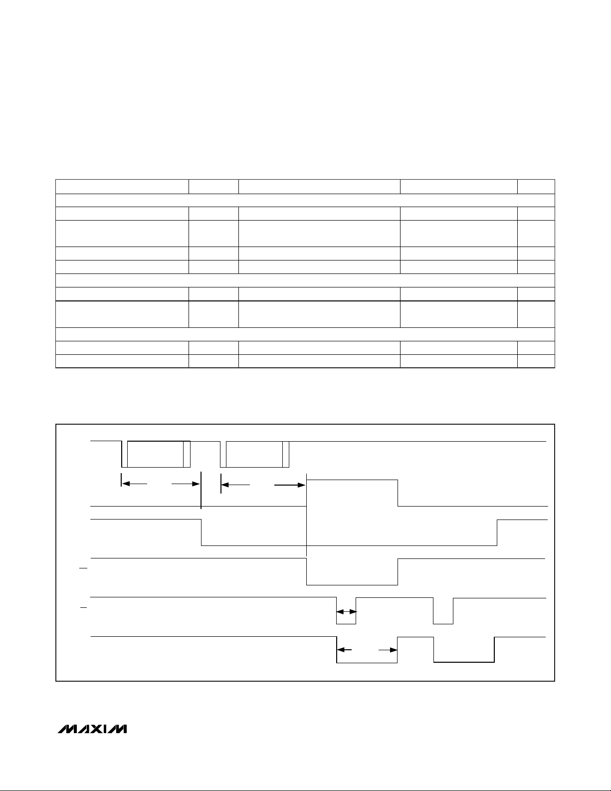
Figure 1. Multiplexed Parallel Bus Timing
XTAL1 Cycle Time t
ALE Pulse Width t
Address Valid to ALE Low t
ALE Low to RD or WR Low t
RD Pulse Width t
RD Low to Data Read Valid t
WR/RD High to ALE High t
WR Pulse Width t
Data Write Valid to WR Low t
ALE
CS
PARAMETER S YMBOL CONDITIONS MIN TYP MAX UNITS
50 ns
20 ns
W(ALE)
10 ns
AVLL
10 ns
W(RD)
Register URR 2 x t
Other registers 10
CY(XTAL1)
50 ns
10 ns
10 ns
W(WR)
10 ns
t
(AL-RWL)
t
W(ALE)
t
AVLL
CY(XTAL1)
(AL-RWL)
(RL-DV)
(RWH-AH)
(DV-WL)
ns
D7–D0
RD
WR
ADDRESS ADDRESS
t
W(RD)
t
(RL-DV)
DATA
(READ)
t
(RWH-AH)
t
(DV-WL)
DATA
(WRITE)
t
W(WR)
t
(RWH-AH)
Page 8
DS8007
Multiprotocol Dual Smart Card Interface
8 _______________________________________________________________________________________
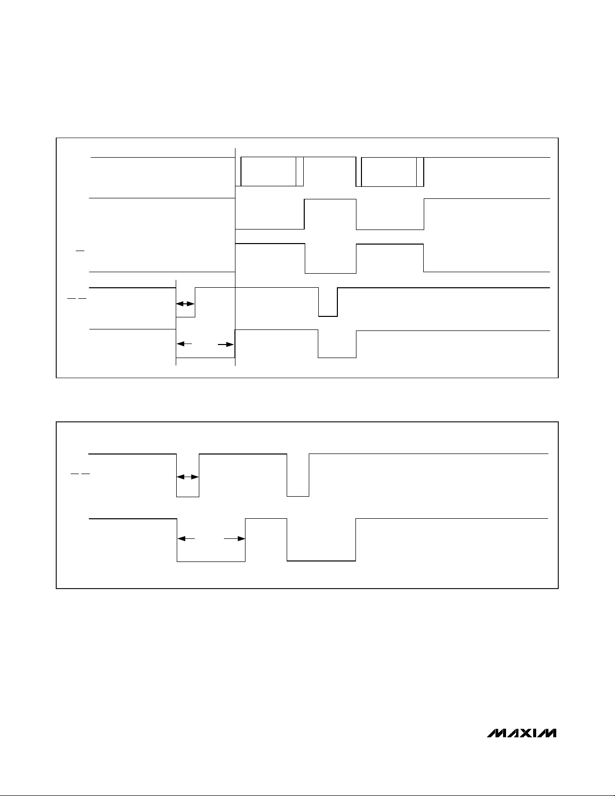
Figure 2. Nonmultiplexed Parallel Bus Timing (Read and Write)
AC ELECTRICAL SPECIFICATIONS—TIMING PARAMETERS FOR NONMULTIPLEXED
PARALLEL BUS (READ AND WRITE)
(VDD= 3.3V, V
DDA
= 3.3V, TA= +25°C, unless otherwise noted.) (See Figure 2.)
RD High to CS Low t
Access Time CS Low to Data Out Valid t
CS High to Data Out High Impedance t
PARAMETER SYMBOL CONDITIONS MIN TYP MAX UNITS
1
2
3
10 ns
50 ns
10 ns
Data Valid to End of Write t
Data Hold Time t
RD Low to CS or WR Low t
Address Stable to CS or WR High t
Address to CS Low t
READ
CS
t
WR (EN)
RD (R/W)
AD3–AD0
D7–D0
WRITE
CS
WR (EN)
1
t
8
4
5
6
7
8
t
2
ADDRESS
DATA OUT
t
3
10 ns
10 ns
10 ns
10 ns
10 ns
WRITE
RELEASE
WITH CS
CS
WR (EN)
t
6
RD (R/W)
t
7
AD3–AD0
D7–D0
ADDRESS
t
4
DATA IN
t
5
WRITE
RELEASE
WITH EN
Page 9
DS8007
Multiprotocol Dual Smart Card Interface
_______________________________________________________________________________________ 9
AC ELECTRICAL SPECIFICATIONS—TIMING PARAMETERS FOR CONSECUTIVE
READ/WRITE TO URR/UTR/TOC
(VDD= 3.3V, V
DDA
= 3.3V, TA = +25°C, unless otherwise noted.)
Figure 3. Timing Between Two Read Operations in Register URR
Note 4: Depends on the leading edge of WR or CS (whichever is deasserted first). Reference this specification to the rising edge
of CS/WR instead of the falling edge.
Note 5: PSC is the programmed prescaler value (31 or 32).
PARAMETER S YMBOL CONDITIONS MIN TYP MAX UNITS
SEE FIGURE 3
RD Pulse Width t
RD Low to Bit CRED = 1 t
Set Time Bit FE t
Set Time Bit RBF t
SEE FIGURE 4
WR/CS Pulse Width t
WR/CS Low to I/Ox Low t
SEE FIGURE 5
WR/CS Pulse Width t
WR/CS High to Bit CRED = 1 t
10 ns
W(RD)
RD(URR)
10.5 ETU
SB(FE)
10.5 ETU
SB(RBF)
(Note 4) 10 ns
W(WR)
WR(UTR)
10 ns
W(WR)
(Notes 4 and 5) 1 / PSC 2 / PSC ETU
WR(TOC)
t
W(RD)
2t
CY(CLK)
t
W(WR)
2t
CY(CLK)
+
+
t
W(RD)
3t
CY(CLK)
t
W(WR)
3t
CY(CLK)
+
+
ns
ns
I/Ox
RBF BIT
FE BIT
INT
RD
CRED BIT
t
SB(FE)
t
SB(RBF)
t
W(RD)
t
RD(URR)
Page 10
DS8007
Multiprotocol Dual Smart Card Interface
10 ______________________________________________________________________________________
Figure 4. Timing Between Two Write Operations in Register UTR
Figure 5. Timing Between Two Write Operations in Register TOC
I/Ox
TBE BIT
INT
WR/CS
CRED BIT
t
W(WR)
t
WR(UTR)
t
WR/CS
CRED BIT
W(WR)
t
WR(TOC)
Page 11
DS8007
Multiprotocol Dual Smart Card Interface
______________________________________________________________________________________ 11
Pin Description
PIN NAME FUNCTION
Reset Output. This active-high output is provided for resetting external devices. The RSTOUT pin is driven
1 RSTOUT
2 I/OAUX Auxiliary I/O. This I/O pin allows connection to an auxiliary smart card interface.
3 I/OA
4 C8A
5 PRESA Smart Card A Presence Contact. This is the active-high presence contact associated with smart card A.
6 C4A
7 GNDA Smart Card A Ground. Thi s must be connected to GND.
8 CLKA
9 V
10 RSTA
11 I/OB
12 C8B
13 PRESB Smart Card B Presence Contact. This is the active-high presence contact associated with smart card B.
14 C4B
15 GNDB Smart Card B Ground. This must be connected to GND.
16 CLKB
17 V
18 RSTB
19 GND Ground
20 VUP Step-Up Converter Connection. Connect a low-ESR capacitor of 220nF between this pin and ground.
21 CPA1 Step-Up Converter Contact 1. Connect a low-ESR capacitor of 220nF between CPA1 and CPA2.
22 CPB1 Step-Up Converter Contact 3. Connect a low-ESR capacitor of 220nF between CPB1 and CPB2.
23 V
CCA
CCB
DDA
high until the DELAY pin reaches V
stated so it can externally b e pul led down. The SUPL bit is set for each RSTOUT pulse.
Smart Card A I/O Data Line. This i s the I/O data line associated with smart card A. This is a lso referred to
as the ISO C7 contact.
Smart Card A Auxiliary I/O. This is an auxiliary I/O associated with smart card A. This is also referred to
as the ISO C8 contact. This can be associated with synchronous cards.
Smart Card A Auxiliary I/O. This is an auxiliary I/O associated with smart card A. This is also referred to
as the ISO C4 contact. This can be associated with synchronous cards.
Smart Card A Cloc k Output. This is the clock output assoc iated with smart card A. This is also referred to
as the ISO C3 contact.
Smart Card A Supply Voltage. This i s the supply voltage output assoc iated with smart card A. This i s al so
referred to as the ISO C1 contact.
Smart Card A Reset. This is the reset output as sociated with smart card A. Thi s is a lso referred to as the
ISO C2 contact.
Smart Card B I/O Data Line. This i s the I/O data line associated with smart card B. This is a lso referred to
as the ISO C7 contact.
Smart Card B Auxiliary I/O. This is an auxiliary I/O associated with smart card B. This is also referred to
as the ISO C8 contact. This can be associated with synchronous cards.
Smart Card B Auxiliary I/O. This is an auxiliary I/O associated with smart card B. This is also referred to
as the ISO C4 contact. This can be associated with synchronous cards.
Smart Card B Cloc k Output. This is the clock output assoc iated with smart card B. This is also referred to
as the ISO C3 contact.
Smart Card B Supply Voltage. This i s the supply voltage output assoc iated with smart card B. This i s al so
referred to as the ISO C1 contact.
Smart Card B Reset. This is the reset output as sociated with smart card B. Thi s is a lso referred to as the
ISO C2 contact.
Analog Supply Voltage. Positive analog-supply voltage for the step-up converter; can be higher but not
lower than V
This pin should be decoupled to AGND with a good quality capacitor.
DD.
. Once the DELAY pin reaches V
DRST
, the RSTOUT pin is three-
DRST
Page 12

DS8007
Multiprotocol Dual Smart Card Interface
12 ______________________________________________________________________________________
Pin Description (continued)
PIN NAME FUNCTION
24 CPB2 Step-Up Converter Contact 4. Connect a low-ESR capacitor of 220nF between CPB1 and CPB2.
25 AGND Analog Ground
26 CPA2 Step-Up Converter Contact 2. Connect a low-ESR capacitor of 220nF between CPA1 and CPA2.
27 VDD Digital Supply Voltage. This pin should be decoupled to GND with a good quality capacitor.
28–35 D0–D7
36 RD
37 WR
38 CS Active-Low Chip-Select Input. This input indicates when the DS8007 is active on the parallel bus.
39 ALE
40 INT Active-Low Interrupt. This output indicate s an interrupt is act ive.
41 INTAUX Auxiliary Interrupt Input. This pin serves as an auxiliary interrupt.
42–45 AD3 –AD0
46, 47
48 DELAY
XTAL2,
XTAL1
8-Bit Digital I/O. This port functions as the data or address/data communication lines between the host
controller and the DS8007 for the nonmultiplexed and multiplexed operating modes, respectively.
Active-Low Paralle l Bus Read Strobe Input. In mu ltiple xed mode, this input i ndicates when the host
processor is reading information from the DS8007. In nonmultiplexed mode, this pin signa ls the current
operation is a read (RD = 1) or a write (RD = 0) when CS and WR are low.
Active-Low Parallel Bus Write Strobe Input. In multiple xed mode, this input indicates when the host
processor is writing information to the DS8007. In nonmultiplexed mode, a low on this pin signals the bus
is engaged in a read or write operation.
Address Latch Enable Input. This signal monitors the ALE signal when the host processor bus is
operating in multiplexed mode. Connect this signal to V
Register Selection Address Inputs. These pins function as the address input lines for the nonmultiplexed
configuration and should be connected to ground or V
Crystal Oscillators. Place a crystal with appropriate load capacitors between these pins if that is the
desired clock source. XTAL1 also acts as an input if there is an external clock source in place of a
crystal.
External Delay Capacitor Connection. Connect a capacitor from thi s pin to ground to set the power-on
reset delay.
when operating in nonmult iplexed mode.
DD
in the mu ltiple xed configuration.
DD
Page 13
DS8007
Multiprotocol Dual Smart Card Interface
______________________________________________________________________________________ 13
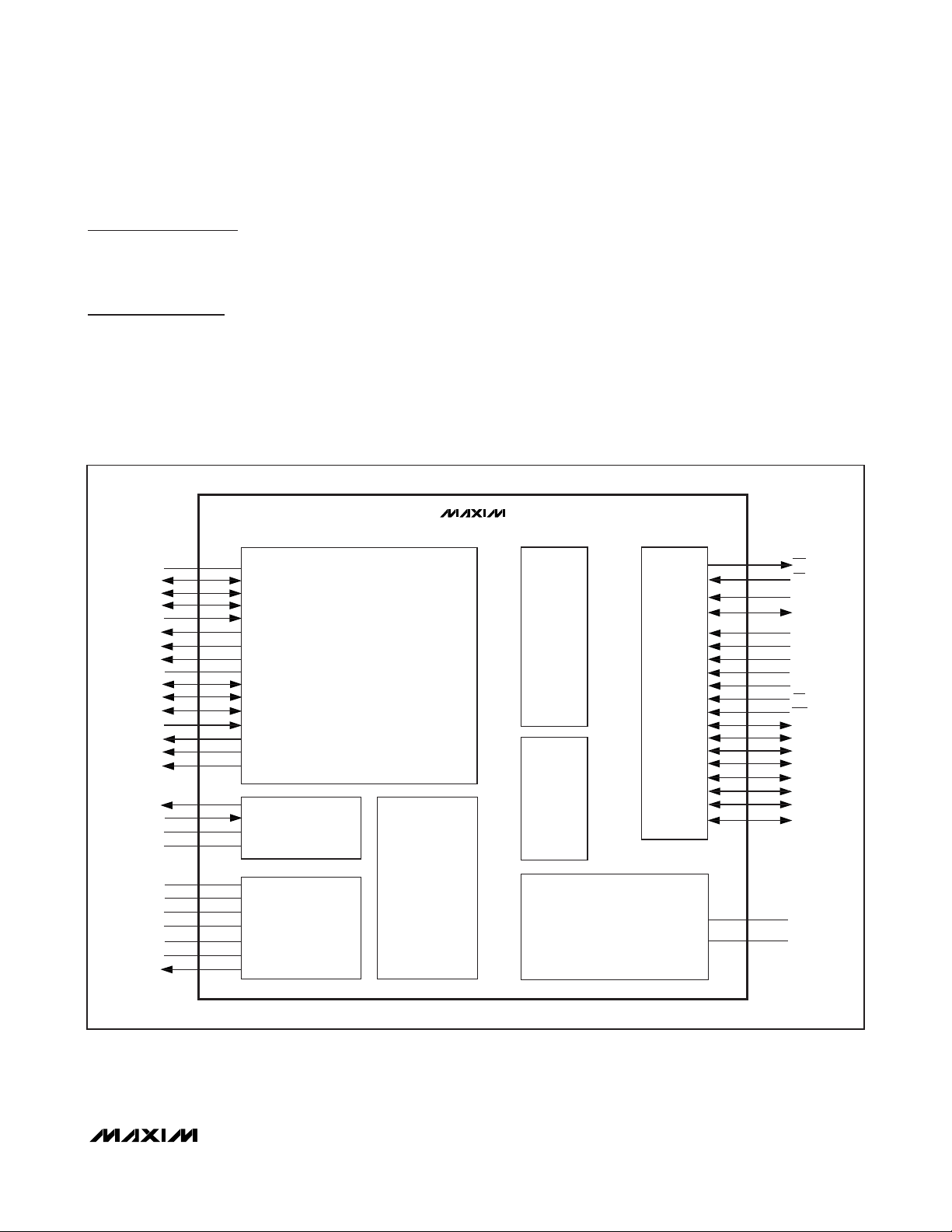
Detailed Description
The following describes the major functional features of
the device. Use of this document requires the reader
have a basic understanding of ISO 7816 terminology.
Parallel Bus Interface
The device interfaces to a host computer/processor
through a multiplexed or demultiplexed, parallel, 8-bit
data bus (D0–D7). The parallel bus interface monitors
the ALE signal and automatically detects whether a
multiplexed or nonmultiplexed external bus interface is
intended. The nonmultiplexed external bus interface is
the default configuration and is maintained so long as
no edge (activity) is detected on the ALE pin. Once a
rising edge is detected on the ALE pin, the DS8007 is
placed into the multiplexed mode of operation. Once in
the multiplexed mode of operation, a reset/power cycle
or the deassertion of CS forces the device to the nonmultiplexed mode. Connecting the ALE pin to V
DD
or
ground forces the device into nonmultiplexed parallel
bus mode. Figure 7 shows that the bus recognition dictates whether the external address lines (AD3–AD0)
can be used directly or whether the external data lines
(D7–D0) must be latched according to the ALE input
signal. In the multiplexed mode of operation, a new
address is latched irrespective of the state of CS.
Figure 6. Block Diagram
GNDB
I/OB
C4B
C8B
PRESB
RSTB
CLKB
V
CCB
GNDA
I/OA
C4A
C8A
PRESA
RSTA
CLKA
V
CCA
RSTOUT
DELAY
V
GND
DD
POWER-SUPPLY
SUPERVISOR
ANALOG
INTERFACE
DS8007
ISO
UART
DIGITAL
INTERFACE
TIMEOUT
COUNTER
INT
CS
INTAUX
I/OAUX
AD0
AD1
AD2
AD3
ALE
RD
WR
D0
D1
D2
D3
D4
D5
D6
D7
CPA1
CPA2
CPB1
CPB2
V
DDA
AGND
V
UP
DC-DC
CONVERTER
CONTROL
SEQUENCERS
CLOCK
GENERATION
XTAL1
XTAL2
Page 14

Multiplexed Mode
In the multiplexed mode of operation, the D7–D0 signals are multiplexed between address and data. The
falling edge of the address latch enable (ALE) signal
from the host microcontroller latches the address
(D3–D0), and the RD and WR strobe input signals are
used to enable a read or write operation, respectively, if
the DS8007 is selected (i.e., CS = 0). See the AC timing
for the multiplexed parallel bus mode found earlier in
this data sheet.
Nomultiplexed Mode
In the nonmultiplexed mode of operation, the address is
always provided on the AD3–AD0 signals, and the data
is always transacted on the D7–D0 signals. The RD input
signal is used as a read/write (R/W) operation select. The
WR and CS input signals serve as active-low enables,
and must be asserted for the read or write operation to
take place. See the AC timing for the nonmultiplexed
parallel bus mode found earlier in this data sheet.
DS8007
Multiprotocol Dual Smart Card Interface
14 ______________________________________________________________________________________
Figure 7. Parallel Bus Interface
CS
RD
WR
REGISTERS
AD3–AD0
D7–D0
ALE
CS
RST
V
LOGIC
OR
DD
RST
LATCH
CONTROL
0
1
D3–D0
Page 15

DS8007
*
u = unchanged, x = always reflects state of external device pin, even when RIU = 0.
Note: Writes to unimplemented bits have no effect. Reads of unimplemented bits return 0.
Table 1. Special Function Register Map
Multiprotocol Dual Smart Card Interface
______________________________________________________________________________________ 15
Control Registers
Special control registers that the host computer/microcontroller accesses through the parallel bus manage
most DS8007 features. Many of the registers, although
only mentioned once in the listing, are duplicated for
each card interface. The PDR, GTR, UCR1, UCR2, and
CCR registers exist separately for each of the three
card interfaces. The PCR register is provided only for
card interface A and card interface B.
The specific register to be accessed is controlled by
the current setting of the SC3–SC1 bits in the Card
Select Register. For example, there are three instances
of the UART Control Register 1 (UCR1) at address 06h.
If the SC3–SC1 bits are configured so that card A is
selected, then all reads and writes to address 06h only
affect card A. If SC3–SC1 are changed to select card
B, then all reads and writes to address 06h only affect
card B, etc.
In addition, some registers have different functions
based on whether the register is being read from or written to. An example of this are the UART Receive
(URR)/UART Transmit (UTR) registers located at address
0Dh. Although they share the same address, during read
operations the receive register is read, and write operations go to a separate transmit register. This selection
requires no extra configuration by the software.
ADDRESS
(HEX)
00 CSR R/W CSR7 CSR6 CSR5 CSR4 RIU SC3 SC2 SC1 0011 0000 0011 0uuu
01 CCR R/W — — SHL CST SC AC2 AC1 AC0 0000 0000 00uu uuuu
02 PDR R/W PD7 PD6 PD5 PD4 PD3 PD2 PD1 PD0 0000 0000 uuuu uuuu
03 UCR2 R/W —
05 GTR R/W GTR.7 GTR.6 GTR.5 GTR.4 GTR.3 GTR.2 GTR.1 GTR.0 0000 0000 uuuu uuuu
06 UCR1 R/W FTE0 FIP — PROT T/R LCT SS CONV 0000 0000 0uuu 00uu
07 PCR R/W — — C8 C4 1V8 RSTIN 3V/5V START 0011 0000 0011 uuuu
08 TOC R/W TO C7 TOC6 TOC5 TOC4 TOC3 TOC2 TOC1 TO C0 0000 0000 000 0 0000
09 TOR1 W TOL7 TOL6 TOL5 TOL4 TOL3 TOL2 TOL1 TOL0 0000 0000 uuuu uuuu
0A TOR2 W TOL15 TOL14 TOL13 TOL12 TOL11 TOL10 TOL9 TOL8 0000 0000 uuuu uuuu
0B TOR3 W TOL23 TOL22 TOL21 TOL20 TOL19 TOL18 TOL17 TOL16 0000 0000 uuuu uuuu
0C MSR R CLKSW FE BGT CRED PRB PRA INTAUX
0C FCR W — PEC2 PEC1 PEC0 FTE1 FL2 FL1 FL0 0000 0000 0uuu 0uuu
0D URR R UR7 UR6 UR5 UR4 UR3 UR2 UR1 U R0 0000 0000 0000 0000
0D UTR W UT7 UT6 UT5 UT4 UT3 UT2 UT1 UT0 0000 0000 0000 0000
0E USR R TO3 TO2 TO1 EA PE OVR FER
0F HSR R — PRTLB PRTLA SUPL PRLB PRLA INTAUXL PTL 0001 0000 0uuu xxxu
REGISTER
NAME
R/W BIT 7 BIT 6 BIT 5 BIT 4 BIT 3 BIT 2 BIT 1 BIT 0 RESET RIU = 0*
DISTBE/
DISAUX PDWN SAN AUTOC CKU PSC 0000 0000 uuuu uuuu
RBF
TBE/
0101 0000 u1u1 uuu0
RBF
TBE/
0000 0000 0000 0000
RBF
Page 16

DS8007
Multiprotocol Dual Smart Card Interface
16 ______________________________________________________________________________________
Card Select Register (CSR)
R = unrestricted read, W = unrestricted write, -n = value after reset. This register is reset to 00110uuub on RIU = 0.
Clock Configuration Register (CCR)
R = unrestricted read, W = unrestricted write, -n = value after reset. This register is reset to 00uuuuuub on RIU = 0.
Bits 7 to 4: Identification Bits (CSR7 to CSR4). These
bits provide a method for software to identify the device
as follows:
0011 = DS8007 revision Ax
Bit 3: Reset ISO UART (RIU). When this bit is cleared
(0), most of the ISO UART registers are reset to their
initial values. This bit must be cleared for at least 10ns
prior to initiating an activation sequence. This bit must
be set (1) by software before any action on the UART
can take place.
Bits 2 to 0: Select Card Bits (SC3 to SC1). These bits
determine which IC card interface is active as shown
below. Only one bit should be active at any time, and
no card is selected after reset (i.e., SC3–SC1 = 000b).
Other combinations are invalid.
000 = No card is selected.
001 = Card A is selected.
010 = Card B is selected.
100 = AUX card interface is selected.
Bits 7 and 6: Reserved.
Bit 5: Stop High or Low (SHL). This bit determines if
the card clock stops in the low or high state when the
CST bit is active. It forces the clock to stop in a low
state when SHL = 0 or in a high state when SHL = 1.
Bit 4: Clock Stop (CST). For an asynchronous card,
this bit allows the clock to the selected card to be
stopped. When this bit is set (1), the card clock is
stopped in the state determined by the SHL bit. When
this bit is cleared (0), the card clock operation is
defined by CCR bits AC2–AC0.
Bit 3: Synchronous Clock (SC). For a synchronous
card, the card clock is controlled by software manipulation of this SC, and the contact CLKx is the copy of
the value in this bit. In synchronous transmit mode, a
write to the UTR results in the least significant bit (LSb)
of the data written to the UTR being driven out on the
I/Ox pin. In synchronous receive mode, the state of the
I/Ox pin can be read from the LSb of the URR.
Bits 2 to 0: Alternating Clock Select (AC2 to AC0).
These bits select the frequency of the clock provided to
the active card interface and to the UART for the elementary time unit (ETU) generation as shown below. All
frequency changes are synchronous so that there are
no spikes or unwanted pulse widths during transitions.
f
INT
is the frequency of the internal oscillator.
AC2–AC0
000 = f
XTAL
001 = f
XTAL
/ 2
010 = f
XTAL
/ 4
011 = f
XTAL
/ 8
1xx = f
INT
/ 2
76543210
Address 00h CSR7 CSR6 CSR5 CSR4 RIU SC3 SC2 SC1
R-0 R-0 R-1 R-1 RW-0 RW-0 RW-0 RW-0
76543210
Address 01h — — SHL CST SC AC2 AC1 AC0
R-0 R-0 RW-0 RW-0 RW-0 RW-0 RW-0 RW-0
Page 17

DS8007
Bits 7 to 0: Programmable ETU Divider Register Bits
7 to 0 (PD7 to PD0). These bits, in conjunction with the
defined UART input clock (based upon CKU,
AC2–AC0) and the prescaler selection (PSC bit), are
used to define the ETU for the UART when interfaced to
the associated card interface. The output of the
prescaler block is further divided according to the
PD7–PD0 bits as follows:
• ETU = Prescaler output / (PD7–PD0), when
PD7–PD0 = 02h–FFh
• ETU = Prescaler output / 1, when PD7–PD0 = 00h–01h
• Prescaler output / 256 is not supported
Programmable Divider Register (PDR)
R = unrestricted read, W = unrestricted write, -n = value after reset; all bits unaffected by RIU = 0.
UART Control Register 2 (UCR2)
R = unrestricted read, W = unrestricted write, -n = value after reset; all bits unaffected by RIU = 0.
Bit 7: Reserved.
Bit 6: Disable TBE/RBF Interrupt (DISTBE/RBF). This
bit controls whether the TBE/RBF flag can generate an
interrupt on the INT pin. When this bit is cleared to 0,
an interrupt is signaled on the INT pin in response to
the TBE/RBF flag getting set. When DISTBE/RBF is set
to 1, interrupts are not generated in response to the
TBE/RBF flag. Disabling the TBE/RBF interrupt can
allow faster communication speed with the card, but
requires that a copy of TBE/RBF in register MSR be
polled to not lose priority interrupts that can occur in
register USR.
Bit 5: Disable Auxiliary Interrupt (DISAUX). This bit
controls whether the external INTAUX pin can generate
an interrupt on the INT output pin. When this bit is
cleared to 0, a change on the INTAUX input pin results
in assertion of the INT output pin. When DISAUX is set
to 1, a change on INTAUX does not result in assertion
of the INT output pin. The INTAUXL bit is set by a
change on the INTAUX pin independent of the DISAUX
bit state. Since the INTAUX bit is set independent of the
DISAUX bit, it is advisable to read HSR (thus clearing
INTAUX) prior to clearing DISAUX to avoid an interrupt
on the INT pin. To avoid an interrupt when selecting a
different card, the DISAUX bit should be set to 1 in all
UCR2 registers.
Multiprotocol Dual Smart Card Interface
______________________________________________________________________________________ 17
76543210
Address 02h PD7 PD6 PD5 PD4 PD3 PD2 PD1 PD0
RW-0 RW-0 RW-0 RW-0 RW-0 RW-0 RW-0 RW-0
76 5 4 3 2 1 0
Address 03h — DISTBE/RBF DISAUX PDWN SAN AUTOC CKU PSC
R-0 RW-0 RW-0 RW-0 RW-0 RW-0 RW-0 RW-0
Page 18

DS8007
Multiprotocol Dual Smart Card Interface
18 ______________________________________________________________________________________
Bit 4: Power-Down Mode Enable (PDWN). This bit
controls entry into the power-down mode. Power-down
mode can only be entered if the SUPL bit has been
cleared. When PDWN is set to 1, the XTAL1 and XTAL2
crystal oscillator is stopped, and basic functions such
as the sequencers are supported by the internal ring
oscillator. The UART is put in a suspended state, and
the clocks to the UART, the ETU unit, and the timeout
counter are gated off. During the power-down mode, it
is not possible to select a card other than the one currently selected (advisory to the programmer, selecting
another card during power-down mode is not recommended). There are five ways of exiting the powerdown mode:
• Insertion of card A or card B (detected by PRLA or
PRLB).
• Withdrawal of card A or card B (detected by PRLA
or PRLB).
• Reassertion of the CS pin to select the DS8007 (CS
must be deasserted after setting PDWN = 1 for this
event to exit from power-down).
• INTAUXL bit is set due to change in INTAUX
(INTAUXL bit must be cleared first).
• Clearing of PDWN bit by software (if CS pin is
always tied to 0).
Except in the case of a read operation of register HSR,
the INT pin remains asserted in the active-low state.
The host device can read the status registers after the
oscillator warmup time, and the INT signal returns to
the high state.
Bit 3: Synchronous/Asynchronous Card Select
(SAN). This bit selects whether a synchronous or asyn-
chronous card interface is enabled. When this bit is
cleared to 0, an asynchronous card interface is expected. When this bit is set to 1, a synchronous interface is
expected. In synchronous mode, the UART is
bypassed; the SC bit controls the CLK, and I/O is transacted in the LSb of UTR/URR. Card interface AUX cannot operate in the true synchronous mode since it does
not have a CLK signal to accompany I/OAUX. However,
the SAN bit invokes the same control of I/OAUX through
UTR/URR as is given for card interfaces A and B.
Bit 2: Auto Convention Disable (AUTOC). This active-
low bit controls whether the decoding convention
should automatically be detected during the first
received character in answer-to-reset (ATR). If AUTOC
= 0, the character decoding convention is automatically
detected (while SS = 1) and the UCR1.CONV bit is written accordingly by hardware. If AUTOC = 1, the
UCR1.CONV bit must be set by software to assign the
character decoding convention. The AUTOC bit must
not be changed during a card session.
Bit 1: Clock UART Doubler Enable (CKU). This bit
enables the effective ETU defined for the UART to last
half the number of clock cycles defined by the
AC2–AC0 and PD7–PD0 configuration (except in the
case when AC2–AC0 = 000b, where f
CLK
= f
XTAL
).
When CKU is cleared to 0, the AC2–AC0 defined f
CLK
is used for ETU timing generation. When CKU is set to
1, a clock frequency of 2 x f
CLK
is used for ETU gener-
ation.
Bit 0: Prescaler Select (PSC). When PSC = 0, the
prescaler value is 31. When PSC = 1, the prescaler
value is 32.
Guard Time Register (GTR)
R = unrestricted read, W = unrestricted write, -n = value after reset; all bits unaffected by RIU = 0.
Bits 7 to 0: Guard Time Register Bits 7 to 0 (GTR.7
to GTR.0). These bits are used for storing the number
of guard time units (ETU) requested during ATR. When
transmitting, the DS8007 UART delays these numbers
of extra guard time ETU before transmitting a character
written to UTR.
76543210
Address 05h GTR.7 GTR.6 GTR.5 GTR.4 GTR.3 GTR.2 GTR.1 GTR.0
RW-0 RW-0 RW-0 RW-0 RW-0 RW-0 RW-0 RW-0
Page 19

DS8007
Multiprotocol Dual Smart Card Interface
______________________________________________________________________________________ 19
UART Control Register 1 (UCR1)
R = unrestricted read, W = unrestricted write, -n = value after reset. This register is reset to 0uuu00uub on RIU = 0.
Bit 7: FIFO Threshold Enable 0 (FTE0). When this bit
and the FTE1 (FCR.3) bit are set, the programmable
FIFO threshold feature is enabled. This bit always
reads 0 for compatibility.
Bit 6: Force Inverse Parity (FIP). When this bit is configured to 0, the correct parity is transmitted with each
character, and receive characters are checked for the
correct parity. When FIP = 1, an inverse parity bit is
transmitted with each character and correctly received
characters are NAK’d.
Bit 5: Reserved. This bit must be left 0. Setting this bit
to 1 causes improper device operation.
Bit 4: Protocol Select (PROT). This bit is set to 1 by
software to select the asynchronous T = 1 protocol and
is cleared to 0 to select the T = 0 protocol.
Bit 3: Transmit/Receive (T/R). This bit should be set
by software to operate the UART in transmit mode.
When this bit is changed from 0 to 1 (UART changed
from receive to transmit mode), hardware sets the
USR.RBF/TBE bit, indicating an empty transmit buffer.
The T/R bit is automatically cleared to 0 following successful transmission if UCR1.LCT is configured to 1
prior to the transmission. This bit cannot be written to
when RIU = 0 (holding in reset).
Bit 2: Last Character to Transmit (LCT). This bit is
optionally set by software prior to writing the last character to be transmitted to the UART transmit register
(UTR). If LCT is set to 1 prior to writing to UTR, hardware resets the LCT, T/R, and TBE/RBF bits following a
successful transmission. Setting this bit to 1 allows
automatic change to the reception mode after the last
character is sent. This bit can be set during and before
the transmission. This bit cannot be written to when RIU
= 0 (holding in reset).
Bit 1: Software Convention Setting (SS). This bit
should be set by software prior to ATR to allow automatic convention detection. Hardware automatically resets
the SS bit at 10.5 ETU after the detection of the start bit
of the first character of the ATR.
Bit 0: Convention (CONV). This bit defines the character decoding convention of the ISO UART. If CONV = 1,
the convention is direct. If CONV = 0, the convention is
inverted. If automatic convention detection is enabled
(AUTOC = 0), hardware detects the character conven-
tion and configures the CONV bit appropriately at 10.5
ETU. Otherwise (AUTOC = 1), software must configure
the CONV bit.
76 5 4 3 2 1 0
Address 06h FTE0 FIP — PROT T/R LCT SS CONV
R-0 RW-0 R-0 RW-0 RW-0 RW-0 RW-0 RW-0
Page 20

DS8007
Multiprotocol Dual Smart Card Interface
20 ______________________________________________________________________________________
Bits 7 to 0: Timeout Counter Configuration Register
Bits (TOC7 to TOC0). These register bits determine
the counting configuration for the three timeout counter
registers. The available configurations are detailed in
the
Timeout Counter Operation
section. These registers
can be written when RIU = 1 before activation and cannot be written to when RIU = 0.
Bits 7 and 6: Reserved.
Bit 5: Contact 8 (C8). Writes to this register bit are out-
put on the C8 pin of the card interface. Reads of this
register bit reflect the value on the C8 pin.
Bit 4: Contact 4 (C4). Writes to this register bit are output on the C4 pin of the card interface. Reads of this
register bit reflect the value on the C4 pin.
Bit 3: 1.8V Card Select (1V8). If this bit is set to 1, the
V
CCx
supplied to the card interface is 1.8V. This bit
overrides the 3V/5V bit.
Bit 2: Reset Bit (RSTIN). When a card interface is activated, the RSTx pin is driven according to the value
contained in this register bit.
Bit 1: 3V/5V Card Select (3V/5V). This bit determines
the V
CCx
level for the card interface. When this bit is set
to 1, V
CCx
is defined as 3V. When this bit is cleared to
0, V
CCx
is defined as 5V. When the 1V8 and 3V/5V bits
are set to 1, priority is given to 1V8.
Bit 0: Start (START). This bit controls software activation/deactivation of the card interface. When this bit is
written to 1, the activation sequence for the selected
card is performed. When this bit is written to 0, the
deactivation sequence for the selected card is performed. Hardware automatically resets the START bit
for the associated card interface when emergency
deactivation occurs. This bit can be written regardless
of the state of the RIU bit.
Power Control Register (PCR)
R = unrestricted read, W = unrestricted write, -n = value after reset. This register is reset to 0011uuuub on RIU = 0.
Note: The AUX card interface does not have register PCR. C4 and C8 are external ports that are internally pulled up (10k
Ω
to V
CCx
),
writing a 1 to C4, C8 configures the weak pullup. Reads are made of the pin state to a different physical bit. Writing a 0 to C4, C8
configures the pulldown. C4 and C8 bits can be written irrespective of the state of the T/R bit.
Timeout Configuration Register (TOC)
R = unrestricted read, W = unrestricted write, -n = value after reset. This register is reset to 00000000b on RIU = 0.
76543210
Address 07h — — C8 C4 1V8 RSTIN 3V/5V START
R-0 R-0 RW-1 RW-1 RW-0 RW-0 RW-0 RW-0
76543210
Address 08h TOC7 TOC6 TOC5 TOC4 TOC3 TOC2 TOC1 TOC0
RW-0 RW-0 RW-0 RW-0 RW-0 RW-0 RW-0 RW-0
Page 21

DS8007
Bits 7 to 0: Timeout Counter Register 2 Bits (TOL15
to TOL8). This register can be configured to operate as
the lower 8 bits of a 16-bit counter or as the middle 8
bits of a 24-bit counter. See the
Timeout Counter
Operation
section for details on configurable modes.
Timeout Counter Register 2 (TOR2)
R = unrestricted read, W = unrestricted write, -n = value after reset. This register is unchanged on RIU = 0.
Timeout Counter Register 3 (TOR3)
R = unrestricted read, W = unrestricted write, -n = value after reset. This register is unchanged on RIU = 0.
Bits 7 to 0: Timeout Counter Register 3 Bits (TOL23
to TOL16). This register can be configured to operate
as the high 8 bits of a 16-bit counter or as the high 8
bits of a 24-bit counter. See the
Timeout Counter
Operation
section for details on configurable modes.
Timeout Counter Register 1 (TOR1)
R = unrestricted read, W = unrestricted write, -n = value after reset. This register is unchanged on RIU = 0.
Bits 7 to 0: Timeout Counter Register 1 Bits (TOL7 to
TOL0). This register can be configured to operate as an
8-bit counter or as the lowest 8 bits of a 24-bit counter.
TOR1, TOR2, and TOR3 are concatenated to form a 24bit ETU counter or a pair of independent 16- and 8-bit
counters. These counters are only used when a card is
supplied an active clock. See the
Timeout Counter
Operation
section for details on configurable modes.
Multiprotocol Dual Smart Card Interface
______________________________________________________________________________________ 21
76543210
Address 09h TOL7 TOL6 TOL5 TOL4 TOL3 TOL2 TOL1 TOL0
W-0 W-0 W-0 W-0 W-0 W-0 W-0 W-0
76543210
Address 0Ah TOL15 TOL14 TOL13 TOL12 TOL11 TOL10 TOL9 TOL8
W-0 W-0 W-0 W-0 W-0 W-0 W-0 W-0
76543210
Address 0Bh TOL23 TOL22 TOL21 TOL20 TOL19 TOL18 TOL17 TOL16
W-0 W-0 W-0 W-0 W-0 W-0 W-0 W-0
Page 22

DS8007
Multiprotocol Dual Smart Card Interface
22 ______________________________________________________________________________________
Mixed Status Register (MSR)
R = unrestricted read, W = unrestricted write, -n = value after reset. This register is reset to u1u1uuu0b on RIU = 0.
Bit 7: Clock Switch (CLKSW). This status bit indicates
the clock (f
XTAL
/ n or f
INT
/ 2) being sourced by the
selected card interface and thus may be used to determine when a requested clock switch has occurred
properly. When CLKSW is set 1, the clock has switched
from f
XTAL
/ n to f
INT
/ 2; when CLKSW is cleared to 0,
the clock has switched from f
INT
/ 2 to f
XTAL
/ n.
Bit 6: FIFO Empty Status Bit (FE). This bit is set to 1
when the receive FIFO is empty. This bit is cleared to 0
when at least one character remains in the receive FIFO.
Bit 5: Block Guard Time Status Bit (BGT). This status
bit is linked to an ETU counter for the currently selected
card interface, and is intended for use in verifying that
the block guard time is always being met. The counter
restarts on every start bit and stops only if the terminal
count is reached. The terminal count is dependent
upon the selected protocol (16 ETU for T = 0 and 22
ETU for T = 1). This bit is cleared to 0 on every start bit.
Bit 4: Control Ready (CRED). This bit signals the host
device that the DS8007 is ready to handle the next
write operation to UTR or TOC or the next read operation of URR. When CRED = 0, the DS8007 is still working on the previous operation and cannot correctly
process the new read/write request. When CRED = 1,
the DS8007 is ready for the next read/write request.
This “busy” bit allows the DS8007 to meet the timing
constraints of high-speed host devices. The CRED bit
remains low:
• 3 clock cycles after the rising edge of RD before
reading URR.
• 3 clock cycles after the rising edge of WR (or CS)
before writing to UTR.
• 1/PSC (min) ETU and 2/PSC (max) ETU after the
rising edge of WR (or CS) before writing to TOC
The CRED bit timing applies to asynchronous mode
only; this bit is forced to 1 in synchronous mode.
Bit 3: Presence Card B (PRB). This bit is set to 1 when
card B presence is detected and is cleared to 0 when
card B is not present.
Bit 2: Presence Card A (PRA). This bit is set to 1 when
card A presence is detected and is cleared to 0 when
card A is not present.
Bit 1: INTAUX Bit (INTAUX). This bit reflects the state
of the INTAUX pin. This bit is set when the INTAUX pin
is high and is cleared when the INTAUX pin is low.
Bit 0: Transmit Buffer Empty/Receive Buffer Full
(TBE/RBF). This bit signals special conditions relating
to the ISO UART and associated hardware. This bit is
not set when the last character is transmitted by the
UART when LCT = 1.
This bit is set to 1 when:
• UCR1.T/R is changed from 0 (receive mode) to 1
(transmit mode).
• A character is transmitted by the UART.
• The receive FIFO becomes full.
This bit is cleared to 0 when:
• The ISO UART is reset by RIU = 0.
• A character is written to the UART transmit register
(UTR) in transmit mode.
• A character is read from the receive FIFO in
receive mode.
• UCR1.T/R is changed from 1 (transmit mode) to 0
(receive mode).
76543210
Address 0Ch CLKSW FE BGT CRED PRB PRA INTAUX TBE/RBF
R-0 R-1 R-0 R-1 R-0 R-0 R-0 R-0
Page 23

DS8007
UART Receive Register (URR)/UART Transmit Register (UTR)
R = unrestricted read, W = unrestricted write, -n = value after reset. This register is reset to 00000000b on RIU = 0.
FIFO Control Register (FCR)
R = unrestricted read, W = unrestricted write, -n = value after reset. This register is reset to 0uuu0uuub on RIU = 0.
Bits 7 to 0: UART Receive Register (Read
Operations)/UART Transmit Register (Write
Operations) (UR7/UT7 to UR0/UT0). This register is
used both as the UART transmit and receive buffer by the
host microcontroller. Received characters are always
read by the host microcontroller in direct convention,
meaning that if the CONV bit is 0, then characters
received using inverse convention are automatically
translated by the hardware. When the receive FIFO is
enabled, reads of URR always access the oldest available received data. For the synchronous mode of operation, the LSb (URR.0) reflects the state of the selected
card I/Ox line.
Writes by the host microcontroller to this register transmit characters to the selected card. The host microcontroller should write data to UTR in direct convention
(inverse convention encoding is handled by the hardware). The UTR register cannot be loaded during transmission. The transmission:
• Starts at the end of the write operation (rising edge
of WR) if the previous character has been transmit-
ted and the extra guard time has been satisfied.
• Starts at the end of the extra guard time if that
guard time has not been satisfied.
• Does not start if the transmission of the previous
character is not completed (e.g., during retransmission attempts or if a transmit parity error occurs).
For the synchronous mode of operation, only the LSb
(UTR.0) of the loaded data is transferred to the I/Ox pin
for the selected card.
Bit 7: Reserved.
Bits 6 to 4: Parity Error Count (PEC2 to PEC0). These
bits are used only for the T = 0 protocol to determine the
number of retransmission attempts that can occur in
transmit mode and the number of parity errors that can
occur before the PE bit is set to 1 to indicate that the parity error limit has been reached. In transmit mode, the
DS8007 attempts to retransmit a character up to
(PEC2–PEC0) times (when NAK’d by the card) before
the PE bit is set. Retransmission attempts are automatically made at 15 ETU from the previous start bit. If
PEC2–PEC0 = 000b, no retransmission attempt is made,
however, the host device can manually rewrite the character to UTR (in which case, it is re-sent as early as 13.5
ETU from the previous start bit of the error character).
In receive mode, if (PEC2–PEC0 + 1) parity errors have
been detected, the USR.PE bit is set to 1. For example,
if PEC2–PEC0 = 000b, only one parity error needs to be
detected for the PE bit to be set; if PEC2–PEC0 = 111b,
8 parity errors must be detected, etc. If a character is
correctly received before the allowed parity error count
is reached, the parity counter is reset. For the T = 1
protocol, the parity counter is not used. The PE bit is
set whenever a parity error is detected for a received
character.
Bit 3: FIFO Threshold Enable 1 (FTE1). When this bit
and the FTE0 (UCR1.7) bit are set, the programmable
FIFO threshold feature is enabled. This bit always reads
0 for compatibility.
Bits 2 to 0: FIFO Length (FL2 to FL0). These bits
determine the depth of the receive FIFO. The receive
FIFO has depth equal to (FL2–FL0) + 1 (e.g., FIFO
depth = 2 if FL2–FL0 = 001b).
Multiprotocol Dual Smart Card Interface
______________________________________________________________________________________ 23
76543210
Address 0Ch — PEC2 PEC1 PEC0 FTE1 FL2 FL1 FL0
W-0 W-0 W-0 W-0 W-0 W-0 W-0 W-0
76543210
Address 0Dh UR7/UT7 UR6/UT6 UR5/UT5 UR4/UT4 UR3/UT3 UR2/UT2 UR1/UT1 UR0/UT0
RW-0 RW-0 RW-0 RW-0 RW-0 RW-0 RW-0 RW-0
Page 24
DS8007
Multiprotocol Dual Smart Card Interface
24 ______________________________________________________________________________________
Bits 7 to 5: Timeout Counter 3/2/1 Status (TO3 to
TO1). These bits are set to 1 whenever their respective
timeout counter reaches its terminal count. Any of these
bits causes the INT pin to be asserted.
Bit 4: Early Answer Detected (EA). This bit is set to 1
if a start bit is detected on the I/O line during the ATR
between clock cycles 200–368 when the RSTx pin is
low, and during the first 368 clock cycles after the RSTx
pin is high. When the EA bit becomes set, INT is asserted. If the EA bit is set for a card during ATR, this bit is
cleared when switched to another card. During the
early answer detection period, a 46-clock-cycles sampling period should be used to detect the start bit;
there is an undetected period of 32 clock cycles at the
end for both cases (between clock cycles 200–368
when the RSTx pin is low, and the first 368 clock cycles
after the RSTx pin is high).
Bit 3: Parity Error (PE). This status bit indicates when
the transmit or receive parity error count has been
exceeded. For protocol T = 0, the PEC2–PEC0 bits
define the allowable number of transmit or receive parity errors. For protocol T = 1, any parity error results in
the setting of the PE bit. When the PE bit is set, INT is
asserted. For protocol T = 0, characters received with
the incorrect parity are not stored in the receive FIFO.
For protocol T = 1, received characters with parity
errors are stored to the receive FIFO regardless of the
parity bit. The PE bit is set at 10.5 ETU in reception
mode and at 11.5 ETU in transmit mode for T = 0 and T
= 1 (PE bit is not applicable for transmit for T = 1).
Bit 2: Overrun FIFO (OVR). This status bit is set to 1 if
the UART receives a new character when the receive
FIFO is full. When a FIFO overrun condition occurs, the
new character received is lost and the previous FIFO
content remains undisturbed. When the OVR status bit
is set, INT is asserted. The OVR bit is set at 10.5 ETU in
receive mode for T = 0 and T = 1.
Bit 1: Framing Error (FER). This status bit is set to 1 if
the I/O line is not in the high state at time = 10.25 ETU
after the start bit. The FER bit is set to 10.5 ETU in
receive mode for T = 0 and T = 1.
Bit 0: Transmit Buffer Empty/Receive Buffer Full
(TBE/RBF). This is a duplicate of the same status bit
contained in the Mixed Status Register (MSR).
UART Status Register (USR)
R = unrestricted read, W = unrestricted write, -n = value after reset. All register bits are reset to 00000000b on RIU = 0.
Note: If any of the bits TO3, TO2, TO1, EA, PE, OVR, or FER are set, then a USR read operation clears the bit, causing an interrupt
less than 2µs after the rising edge of the RD strobe. PE and FER can be set by the same reception.
76543210
Address 0Eh TO3 TO2 TO1 EA PE OVR FER TBE/RBF
R-0 R-0 R-0 R-0 R-0 R-0 R-0 R-0
Page 25

DS8007
Hardware Status Register (HSR)
R = unrestricted read, W = unrestricted write, -n = value after reset, x = always reflects state of external device pin. This register is
reset to 0uuuxxxub on RIU = 0.
Note: A minimum of 2µs is needed between successive reads of the HSR to allow for hardware updates. In addition, a minimum of
2µs is needed between reads of the HSR and activation of card A, card B, or the AUX card.
Bit 7: Reserved.
Bit 6: Protection Card Interface B Status Bit
(PRTLB). This bit is set to 1 when a fault has been
detected on card reader interface B. A fault is defined
as detection of a short-circuit condition on either the
RSTB or V
CCB
pin as given by DC specs I
RST(SD)
and
I
CC(SD)
. The INT signal is asserted at logic 0 (active)
while this bit is set. This bit returns to 0 after any HSR
read, unless the condition persists.
Bit 5: Protection Card Interface A Status Bit
(PRTLA). This bit is set to a 1 when a fault has been
detected on card reader interface A. A fault is defined
as detection of a short-circuit condition on either the
RSTA or V
CCA
pin as given by DC specs I
RST(SD)
and
I
CC(SD).
The INT signal is asserted at logic 0 (active)
while this bit is set. This bit returns to 0 after any HSR
read, unless the condition persists.
Bit 4: Supervisor Latch (SUPL). This bit is set to 1
when VDD< V
RST
or when a reset is caused by exter-
nally driving the DELAY pin < 1.25V. At this time the
INT signal is asserted at logic 0 (active). This bit returns
to 0 only after an HSR read outside the alarm pulse.
Bit 3: Presence Latch B (PRLB). This bit is set to 1
when a level change has been detected on the PRESB
pin of card interface B. The INT signal is asserted at
logic 0 (active) while this bit is set. This bit returns to 0
after any HSR read.
Bit 2: Presence Latch A (PRLA). This bit is set to 1
when a level change has been detected on the PRESA
pin of card interface A. The INT signal is asserted at
logic 0 (active) while this bit is set. This bit returns to 0
after any HSR read.
Bit 1: INTAUX Latch (INTAUXL). This bit is set to 1
when a 0 → 1 or a 1 → 0 level change has been detected on the INTAUX pin. This bit remains set, regardless
of further level changes on the INTAUX pin until cleared
to 0 by any HSR read.
Bit 0: Protection Thermal Latch (PTL). This bit is set
to 1 when excessive heating (approximately +150°C or
greater) is detected. The INT signal is asserted at logic
0 (active) while this bit is set. This bit returns to 0 after
any HSR read, unless the condition persists.
Multiprotocol Dual Smart Card Interface
______________________________________________________________________________________ 25
76543210
Address 0Fh — PRTLB PRTLA SUPL PRLB PRLA INTAUXL PTL
R-0 R-0 R-0 R-1 R-0 R-0 R-0 R-0
Page 26

DS8007
Multiprotocol Dual Smart Card Interface
26 ______________________________________________________________________________________
Card Interface Voltage Regulation
and Step-Up Converter Operation
The VDDand V
DDA
pins supply power to the DS8007.
Voltage supervisor circuitry detects the input voltage
levels and automatically engages a step-up converter if
necessary to generate the appropriate voltages to the
card interfaces according to the control register settings. The conversion process is transparent to the user
and is usually only noticed by changes in the VUPpin
voltage, which reflects the operation of the internal
charge pump. Table 2 elaborates on the V
UP
pin.
The V
DD
and V
DDA
pins must be decoupled externally,
but extra care must be taken to decouple large current
spikes that can occur on the V
DDA
pins because of
noise generated by the cards and internal voltage stepup circuitry.
Voltage Supply Supervision
The voltage supervisor circuitry monitors VDDand
holds the device in reset until V
DD
is at a satisfactory
level. The DELAY pin is an external indicator of the
state of internal power and can also be driven externally to hold the device in a reset state. An external capacitor is usually attached to this pin, defining the time
constant of a power-on delay for the DS8007. When
VDDis below the voltage threshold V
RST
, the charging
path that exists between V
DD
and DELAY is disconnected and a strong pulldown is enabled on the DELAY
pin. Once VDDexceeds V
RST
, the strong pulldown on
the DELAY pin is released and the pullup to V
DD
is
enabled, allowing the external DELAY capacitor to be
charged.
The RSTOUT alarm pin is released (allowing it to be
pulled up externally) whenever the DELAY pin voltage
is less than V
DRST
, whether caused by VDD< V
RST
or
as a result of external hardware pulling the DELAY pin
low. The minimum duration of the RSTOUT pulse (t
W
specification) is defined by the capacitor connected to
the DELAY pin and is typically 1ms per 2nF. The
RSTOUT pin is driven strongly low once the DELAY pin
exceeds the V
DRST
voltage threshold.
The SUPL bit is set on initial power-up and is reset
again when the RSTOUT alarm pulse occurs. The SUPL
bit may only be cleared by a read of the HSR register.
Figure 8 illustrates the sequencing of the various signals involved.
Short-circuit and thermal-protection circuitry prevent
damages done by accidentally shorting the V
CCx
pins
or when the ambient temperature is exceeding the
maximum operating temperature. When the internal
temperature is approximately +150°C, the voltage V
CCx
and the drivers to the CLKx, RSTx, I/Ox, C4x, and C8x
signals to both card interfaces are turned off. The PTL
bit in the HSR is set and an interrupt is generated.
When a short is detected on the RSTx pin, the device
initiates a normal deactivation sequence. A short on
I/Ox, C4x, and C8x does not cause deactivation.
Table 2. Step-Up Converter Operation
VOLTAGE (V)
V
DDA
< 2.4 X V
2.4–3.5 5 5.7
3.5–5.5 5 5.7
5.5–6.0 5 V
2.4–3.5 3.0 4.1
> 3.5 3.0 V
2.4–6.0 1.8 V
SMART CARD V
UP
DDA
DDA
DDA
DDA
Page 27

DS8007
V
Figure 8. Voltage Supervisor
Multiprotocol Dual Smart Card Interface
______________________________________________________________________________________ 27
DELAY
RSTOUT
V
= 2.1V TO 2.5V
RST
INT
DD
= ~1.25V
V
DRST
t
W
RESULTING FROM
< V
V
DD
RST
DELAY DRIVEN
LOW EXTERNALLY
SUPL BIT
SUPL BIT CLEARED BY HSR READ ONLY
Page 28

DS8007
Multiprotocol Dual Smart Card Interface
28 ______________________________________________________________________________________
Figure 9. Card Activation, Deactivation Sequences
Activation Sequencing
An activation sequence can only be requested by a
host device through the parallel bus interface. The host
can request an activation sequence for a specific card
(card A or card B) by setting the START bit of the PCRx
register (where x = A or B as determined by the card
select SCx bits of the CSR). The host software can activate both cards at the same time, but only one card
can be selected to transmit/receive at a given time. The
activation sequence can only occur given satisfactory
operating conditions (e.g., the card is present and the
supply voltage is correct). These conditions can be
ascertained through the HSR, MSR, and CSR bits.
If the microcontroller attempts to write the PCRx.START
bit to 1 without having satisfied the necessary conditions, the card is not activated and the bit does not
change. The activation time (from the assertion of the
START bit until the clock output is enabled) is less than
130µs. The activation sequence is detailed in Figure 9.
ACTIVATION SEQUENCE DEACTIVATION SEQUENCE
1234 5 12 3 45 66
START BIT
RSTIN BIT
RSTx
V
V
CCx
UP
ACTIVATION NEEDS TO OCCUR IN UNDER 130μs
V
NEEDS TO DECREASE TO LESS THAN 0.4V
CCx
CLKx
I/0x
C4x, C8x
TIMING
ACTIVATION SEQUENCE
1. PCRx.START BIT IS SET BY SOFTWARE.
CONDITIONS NEEDED (IN HARDWARE) ARE:
MSR.PRx = 1 (CARD x PRESENT)
HSR.PRTLx, SUPL, PRLx, PTL = 0
2. STEP-UP CONVERTER ACTIVATED (MAY ALREADY BE ON IF ANOTHER CARD WAS ACTIVE).
3. V
CCx
V
CCx
4. I/Ox IS PULLED HIGH. C4x, C8x ARE ALSO PULLED HIGH IF PCRx.C4 = 1, PCRx.C8 = 1
(RESPECTIVELY). THESE PINS HAVE INTEGRATED PULLUPS (14kΩ FOR I/Ox AND
10kΩ FOR C4x AND C8x) TO V
5. CLKx OUTPUT IS ENABLED AND RST OUTPUT IS ENABLED.
(PCRx.RSTIN SHOULD BE "0" FOR ACTIVE-LOW RSTx.)
6. PCRx.RSTIN WRITTEN TO "1" BY SOFTWARE AFTER USING TOC TO TIME SUFFICIENT
DURATION OF RSTx PIN ASSERTION.
t0 t1 t2 t3 t4 t5 t10 t11 t12 t13 t14 t15
t
ACT
ENABLED TO 1.8V, 3V, OR 5V AS SELECTED BY PCRx.1V8 AND PCR.3V/5V BITS.
RISES FROM 0V TO 1.8V, 3V, OR 5V WITH A CONTROLLED RISE TIME OF 0.17V/μs TYPICAL.
.
CCx
UNDEFINED TS T0
ACCORDING TO PCRx.C4, PCRx.C8 BITS
t
DE
DEACTIVATION SEQUENCE
1. PCRx.START BIT IS CLEARED BY SOFTWARE.
2. THE ACTIVE-LOW RSTx SIGNAL IS ASSERTED BY SOFTWARE.
3. THE CLKx SIGNAL IS STOPPED.
4. I/Ox, C4x, AND C8x FALL TO 0V.
IS DISABLED AND FALLS TO 0V WITH A TYPICAL RATE OF 0.17V/μs.
5. V
CCx
6. STEP-UP CONVERTER IS DEACTIVATED IF NOT IN USE BY ANOTHER CARD AND
PINS CLKx, RSTx, I/Ox, AND V
BECOME LOW IMPEDANCE TO GROUND.
CCx
Page 29

DS8007
Deactivation Sequencing
The host device can request a deactivation sequence
by resetting the START bit to 0 for the desired card
interface. The deactivation (from the deassertion of the
START bit, step 1 of the deactivation sequence, to
V
CCx
decrease to less than 0.4V) is less than 150µs.
Emergency Deactivation
An emergency deactivation occurs if unsatisfactory
operating conditions are detected. An emergency deactivation occurs for all activated cards in response to a
supply-voltage brownout condition (as reported by the
HSR.SUPL bit) or chip overheating (as reported by
HSR.PTL). Emergency deactivation of an individual card
can occur if a short-circuit condition is detected on the
associated V
CCx
or RSTx pin (as reported by
HSR.PRTLx) or in the case of a card takeoff (as reported
by HSR.PRLx). When an emergency deactivation occurs,
hardware automatically forces the associated START
bit(s) to the 0 state. The response of the device to the
emergency deactivation varies according to the source.
If the RSTx pin is shorted or the device overheats, the
sequencer executes a fast emergency deactivation
sequence, which ramps down V
CCx
immediately.
If the V
CCx
pin was shorted, the sequencer executes a
deactivation sequence in same way as if the START bit
was cleared to 0.
Interrupt Generation
The INT output pin signals the host device that an event
occurred that may require attention. The assertion of
the INT pin is a function of the following sources:
• A fault has been detected on card interfaces
(A or B).
•V
DD
has dropped below the acceptable level.
• A reset is caused by externally driving the DELAY
pin to less than 1.25V.
• Excessive heating is detected (i.e., PTL = 1).
• A level change has been detected on pin PRESx or
INTAUX for the card interfaces (A, B, or AUX).
• The parity and/or frame error is detected.
• The early answer (EA) bit is set during ATR.
• The timeout counter(s) reach their terminal
count(s).
• The FIFO full status is reached.
• The FIFO overrun occurs.
• The transmit buffer is empty.
Figure 10. Interrupt Sources
Multiprotocol Dual Smart Card Interface
______________________________________________________________________________________ 29
HSR.PRTLA
HSR.PRLA
HSR.PRTLB
HSR.PRLB
HSR.SUPL
HSR.PTL
HSR.INTAUXL
UCR2A.DISAUX
UCR2B.DISAUX
UCR2AUX.DISAUX
SCA, SCB, SCAUX
USR.TO3
USR.TO2
USR.TO1
USR.EA
USR.PE
USR.OVR
USR.FER
USR.TBE/RBF
UCR2A.DISTBE/RBF
UCR2B.DISTBE/RBF
UCR2AUX.DISTBE/RBF
SCA, SCB, SCAUX
INTERRUPT
GENERATION
INT OUTPUT PIN
Page 30

DS8007
Multiprotocol Dual Smart Card Interface
30 ______________________________________________________________________________________
Timeout Counter Operation
The timeout counter assists the host device in timing
real-time events associated with the communication protocols: the Work Wait Time (WWT), Block Waiting Time
(BWT), etc. The timeout counter registers count ETUs, so
the input clock to the timeout counter is derived from the
output of the programmable divided clock (per card PDR
register). The timeout counter requires the card be powered and have an active clock.
The timeout counter can operate as a single 24-bit
counter (TOR3–TOR1) or as separate 16-bit
(TOR3–TOR2) and 8-bit (TOR1) counters. The timeout
counters can be operated in either software mode or
start bit mode. The software mode is supported for the
16-bit and 24-bit counters. The start-bit mode is supported for all counter widths (8 bit, 16 bit, and 24 bit).
See Table 3.
Software Mode
In software mode, software configures the counter to a
starting value (while stopped) and starts the down
counter by writing the configuration value to the TOC
register. When the terminal count is reached (0h), the
counter stops, the timeout flag is set, and an interrupt is
generated. If the software counter does not reach the
terminal count, it must be stopped before loading a
new value into the associated TORx counter registers.
It is possible to stop and start the 16-bit software
counter while leaving the 8-bit counter enabled (e.g.,
TOC = 65h ↔ 05h, TOC = E5h ↔ 85h, etc.).
If a compatible software mode command is written to the
TOC register before the terminal count is reached (e.g.,
write 61h to TOC register while the 65h TOC command is
running or vice versa), the new command is ignored (still
software mode), but the TOC register is updated with the
new command, and the counter continues to count until
the terminal count is reached, the respective timeout
flag(s) is set, and an interrupt is generated.
Start-Bit Mode
When configured to start-bit mode, counting starts (and
restarts for the 16-bit and 24-bit counters) when a
START bit is detected on the active card interface I/Ox
pin. When the terminal count is reached, the 8-bit
autoreload counter begins counting from the previously
programmed start value, while a 16-bit counter or 24-bit
counter stops when terminal count is reached. If the
terminal count is reached, the timeout flag is set and an
interrupt is generated. The 8-bit autoreload TOR1 register cannot be modified during a count. The 16-bit and
24-bit counter registers can be modified during a count
without affecting the current count. The new register
data is used on the next START bit detection.
Table 3. Timeout Counter Configurations
TOC VALUE TOR3 TOR2 TOR1 DESCRIPTION
00h Stopped
05h Stopped
61h Software Stopped
65h Software
68h Software
Start
Bit/Autoreload
Start
Bit/Autoreload
All counters are stopped.
Counters 3 and 2 are stopped. Counter 1 continues in startbit/autoreload mode for both transmission and reception.
Counter 1 is stopped. Counters 3 and 2 form a 16-bit counter
operating in software mode. The counter is stopped by writing 00h to
the TOC register, and must be stopped before reloading new values
in TOR3 and TOR2 registers.
Counters 3 and 2 form a 16-bit counter operating in software mode.
Writing 05h to the TOC register before reloading new values in
TOR2/TOR3 stops the counters. Counter 1 is operated in startbit/autoreload mode. The TOR1 register may not change during the
count. The 16-bit counters are stopped by setting TOC = 05h. Both
counters are stopped by setting TOC = 00h.
Counters 1, 2, and 3 form a 24-bit counter operating in software
mode. The counter starts after the command is written to the TOC
register, and is stopped by setting TOC = 00h. TOR3, TOR2, TOR1
cannot be changed without stopping the counter first.
Page 31

DS8007
Table 3. Timeout Counter Configurations (continued)
Multiprotocol Dual Smart Card Interface
______________________________________________________________________________________ 31
TOC VALUE TOR3 TOR2 TOR1 DESCRIPTION
Counter 1 is stopped. Counters 3 and 2 form a 16-bit counter
operating in start bit mode for both transmission and reception.
71h Start Bit Stopped
75h Start Bit
7Ch Start Bit
85h Stopped
E5h Software
Start Bit/Autostop
F1h
F5h
(RCV);
Start Bit (XMT)
Start Bit/Autostop
(RCV);
Start Bit (XMT)
Start
Bit/Autoreload
Start
Bit/Autostop
(RCV);
Start
Bit/Autoreload
(XMT)
Start
Bit/Autostop
(RCV);
Start
Bit/Autoreload
(XMT)
Stopped
Start
Bit/Autostop
(RCV);
Start
Bit/Autoreload
(XMT)
TOR3 and TOR2 registers can be changed during the count, the
current count is not affected, and the values are taken into account
at the next START bit detected on the I/Ox pin. Setting TOC = 00h
stops the counters.
Counter 1 is an 8-bit counter in start-bit/autoreload mode for both
transmission and reception; counters 3 and 2 form a 16-bit counter
operating in start-bit mode for both transmission and reception. The
TOR1 register is not allowed to change during the count. TOR3,
TOR2 registers can be changed during the count, the current count
is not affected, and the values are taken into account at the next
START bit detected on the I/Ox pin. Setting TOC = 00h stops the
counters.
Counters 1/2/3 form a 24-bit counter operating in start-bit mode in
both transmission and reception. TOR3, TOR2 and TOR1 registers
can be changed during the count, the current count is not affected,
and the value is taken into account at the next START bit detected on
the I/Ox pin. Setting TOC = 00h stops the counter.
Counters 3 and 2 are stopped. Counter 1 is operated in startbit/autostop mode in reception and is stopped at the end of the 12th
ETU following the first received START bit detected on the I/Ox pin
unless the terminal count is reached first. Counter 1 operates in startbit/autoreload mode in transmission.
Counters 3 and 2 form a 16-bit counter operating in software mode.
The counters are stopped by setting TOC = 05h before reloading
new values in TOR3 and TOR2 registers. Counter 1 is operated in
autostop mode in reception and is stopped at the end of the 12th
ETU following the first received START bit detected on the I/Ox pin
unless the terminal count is reached first. Counter 1 is operated in
start-bit/autoreload mode in transmission.
Counter 1 is stopped. Counters 3 and 2 form a 16-bit counter. The
16-bit counter is operated in start-bit/auto-stop mode in reception
and is stopped at the end of the 12th ETU following the first received
START bit detected on the I/Ox pin unless the terminal count is
reached first; and the 16-bit counter is operated in start-bit mode in
transmission.
Counter 1 is an 8-bit counter operating in start-bit/autostop mode in
reception and is stopped at the end of the 12th ETU following the
first received START bit detected on the I/Ox pin unless the terminal
count is reached first; and the 8-bit counter is operated in startbit/autoreload mode in transmission. Counters 3 and 2 form a 16-bit
counter operating in start-bit mode for transmission but operate in
start-bit/autostop mode in reception. Counters 3 and 2 are stopped
at the end of the 12th ETU following the first received START bit
detected on the I/Ox pin unless the terminal count is reached first;
the counters are stopped by setting TOC = 00h.
Page 32

DS8007
Multiprotocol Dual Smart Card Interface
32 ______________________________________________________________________________________
ISO UART Implementation
Reset Operation
The CSR.RIU control bit resets the ISO UART. The
CSR.RIU must be reset prior to any activation. CSR.RIU
must be returned to 1 by software before any UART
action can take place.
Synchronous Mode
The synchronous mode of operation is invoked by setting the synchronous/asynchronous card select bit (for
a given card interface) to logic 1. In the synchronous
mode of operation, the associated I/Ox card interface
data is transferred by the LSb of the UART
transmit/receive registers (UTR and URR). In this mode,
the host device using the CCRx.SC register bit manually controls the CLKx pin for the selected card interface.
Switching to the synchronous mode or vice versa is
allowed at any time when the card is active. However, it
is the responsibility of the host software/firmware to
ensure that the current transmission is concluded
before switching. If software configures an active card
for synchronous mode, and then activates another
card, the I/O pin on the previously active card goes to a
high-impedance state with a weak pullup (high). The
newly selected interface (if configured to synchronous
mode) takes on UTR.0.
The AUX card interface does not have an associated
CLK signal, so the CCRAUX.SC bit does not control an
output signal when the synchronous mode of operation
is in effect. The handshake between the host and the
auxiliary smart card interface is accomplished through
the auxiliary interrupt input (INTAUX) and the INT pins.
The MSR.INTAUX bit reflects the state of the INTAUX pin.
If the UCR2.DISAUX bit is cleared to 0, a change on the
INTAUX input pin results in the assertion of INT output
pin. The host software/firmware establishes the communication protocol and controls when to transmit/receive
data in response to the interrupt. If the UCR2.DISAUX bit
is set to 1, the INT pin is not asserted, and the host software/firmware must examine the INTAUX bit in the MSR
register and responds accordingly.
Asynchronous Mode
The asynchronous mode of operation is the reset
default mode for all card interfaces and is selected
when the synchronous/asynchronous card select bit
(for a given card interface) is configured to logic 0. The
I/Ox card interface signal is used for asynchronous
half-duplex data communication between the host-controlled ISO UART and the external smart card. The host
device can optionally stop the CLKx signal in the high
or low state while the card is active using the
CCRx.CST and CCRx.SHL register bits.
ETU Generation and Timing
The basic unit of time for asynchronous mode communication on the I/Ox signal is the elementary time unit
(ETU). The ETU is defined within the ISO UART as a
function of the f
CLK
frequency that is configured for the
card interface (i.e., the same f
CLK
that can be sourced
to the CLKx pin of an associated card interface A or B).
In addition to receiving f
CLK
from the clock generation
block, the ISO UART additionally receives a 2 x f
CLK
frequency if CCRx.AC2–AC0 ≠ 000b. The host device
can select whether f
CLK
or 2 x f
CLK
is used for ETU
generation by using the clock UART (CKU) select bit.
When CKU = 0, f
CLK
is used, while 2 x f
CLK
is used
when CKU = 1. One exception exists when
CCRx.AC2–AC0 = 000b, in which case, only f
CLK
is
sourced to the UART and the CKU bit setting has no
effect on the duration of an ETU.
The basic clock that is selected for ETU generation by
the CKU bit is further prescaled by a factor or 31 or 32.
The prescaler select control (PSC) bit makes this
prescaler selection. When PSC is configured to logic 0,
the prescale setting is 31. When PSC is configured to
logic 1, the prescale setting is 32. The output of the
clock prescaler drives an 8-bit autoreload down
counter. The autoreload value for the downcounter is
configured by the host device through the
Programmable Divider Register (PDR). The interval provided by this downcounter defines the ETU duration for
the selected card. Figure 11 shows a diagram of ETU
generation. All the asynchronous character
transmit/receive operations are defined in terms of ETU
(e.g., 10.5 ETU, 10.25 ETU, etc).
Page 33

DS8007
Standard Clock Frequencies
and Baud Rates
The DS8007 supports I/O communication and CLKx
frequency generation compliant to the following standards: ISO 7816, EMV2000, and GSM11-11. Each of
these standards has an allowable CLKx frequency
range and a defined relationship between CLKx frequency and ETU (baud rate) generation that is supported initially and after negotiation.
For ISO 7816, the relationship between ETU (baud rate)
timing and CLKx frequency is as follows:
ETU = (F / D) x (1 / f
CLKx
)
The minimum CLKx frequency is fixed at 1MHz. The
default maximum CLKx frequency is 5MHz, however,
the maximum CLKx frequency can be increased
according to the Fi parameter given by the card during
ATR. The ISO 7816-1997(3) specification recommends
in Section 4.3.4 that CLKx frequency switches be
made a) immediately after ATR or b) immediately after
a successful PPS exchange. The transmission parameters F and D are respectively the clock-rate conversion
and baud-rate adjustment factors. The notations Fd
and Dd are used to represent the ‘d’efault values for
these parameters, which are Fd = 372 and Dd = 1.
The notation Fi and Di are used to represent the values
‘i’ndicated by the card within the TA(1) character of
ATR. If TA(1) is not present, then Fi, Di are set to the
default Fd, Dd values. The notation Fn and Dn represent values ‘n’egotiated during a successful PPS
exchange, which should be in the range Fd-Fi and DdDi, respectively. During ATR, the default Fd, Dd values
shall apply. If the card comes up in negotiable mode
(i.e., TA(2) is absent from the ATR), then the Fd, Dd
Figure 11. ETU Generation
Multiprotocol Dual Smart Card Interface
______________________________________________________________________________________ 33
f
CLK
2 x f
CLK
0
1
UCR2x.CKU
RSTx
START BIT
CLOCK
PRESCALER
/31: PSC = 0
/32: PSC = 1
UCR2x.PSC
CLOCK
PRESCALER
/31: PSC = 0
/32: PSC = 1
PD7:PD0 =
00h TO FFh
(ALIGNED
ETU GENERATOR)
PD7:PD0 =
00h TO FFh
CLR
GATE
PDR
CLR
PDR
ETU
ETU
0.5 ETU
0.25 ETU
1
0
SOFTWARE
MODE
TOC COUNTERS
EN
CLK
FRACTIONAL ETU
EN
COUNTERS
CLK
FRAME-ERROR-
EN
DETECTED COUNTER
CLK
TO3, TO2,
TO1
10.5 ETU
TO 15 ETU
10.25 ETU
Page 34

DS8007
Multiprotocol Dual Smart Card Interface
34 ______________________________________________________________________________________
parameters continue to be used until a successful PPS
exchange is completed. The negotiated Fn, Dn values
are then used after a successful PPS exchange. If the
card comes up in specific mode (i.e., TA(2) is present
in ATR), then the indicated Fi, Di values apply immediately after successful ATR if bit 5 of the TA(2) character is 0. If bit 5 of TA(2) is 1, implicit values should be
used. The TA(1) character of ATR, if present, contains
the Fi and Di values indicated by the card.
Table 5 demonstrates how the prescaler (PSC) bit and
programmable divider register (PDRx) can be configured to generate the requested F/D ratios. All settings
assume that the CKU bit is configured to its reset
default logic 0 state.
Table 4. Fi, Di Parameter Possibilities
RFU = Reserved for future use.
Table 5. PSC, PDR Settings to Support F, D Parameters
TA(1).Fi Fi MAX CLKx (MHz) Fi = TA(1).Di Di
0000 372 4 31 x 12 0000 RFU
0001 372 5 31 x 12 0001 1
0010 558 6 31 x 18 0010 2
0011 744 8 31 x 24 0011 4
0100 1116 12 31 x 36 0100 8
0101 1488 16 31 x 48 0101 16
0110 1860 20 31 x 60 0110 32
0111 RFU — — 0111 RFU
1000 RFU — — 1000 RFU
1001 512 5 32 x 16 1001 12
1010 768 7.5 32 x 24 1010 20
1011 1024 10 32 x 32 1011 RFU
1100 1536 15 32 x 48 1100 RFU
1101 2048 20 32 x 64 1101 RFU
1110 RFU RFU — 1110 RFU
1111 RFU RFU — 1111 RFU
PSC
TA(1).Fi
0000 0 12 6 3 — — — 1 —
0001 0 12 6 3 — — — 1 —
0010 0 18 9 — — — — — —
0011 0 24 12 6 3 — — 2 —
0100 0 36 18 9 — — — 3 —
0101 0 48 24 12 6 3 — 4 —
0110 0 60 30 15 — — — 53
1001 1 16 8 4 2 1 — — —
1010 1 24 12 6 3 — — 2 —
1011 1 32 16 8 4 2 1 — —
1100 1 48 24 12 6 3 — 4 —
1101 1 64 32 16 8 4 2 — —
0 = /31
1 = /32
0001 0010 0011 0100 0101 0110 1000 1001
PDR SETTING FOR Di =
Page 35

Character Encoding/
Decoding Convention
The ISO UART is designed to support two possible character encoding/decoding formats: direct and inverted.
The direct character coding convention transmits and
receives data LSb first and associates a high logic level
with a bit 1 and a low logic level with a bit 0. The inverse
character coding convention transmits and receives data
most significant bit first and associates a high logic level
with a bit 0 and a low logic level with a bit 1.
The UCR1.CONV bit defines which character convention (CONV = 0:inverse; CONV = 1:direct) should be
used by the ISO UART. The UCR1.CONV bit can be
configured by the host device software or be configured by hardware if automatic convention detection has
been enabled.
Automatic Convention Detection
The automatic convention detection relies upon recognition of a predefined pattern in the first character
received (TS character) in ATR for establishing future
character coding convention. To enable automatic convention detection, the UCR1.SS bit must be set to logic
1 and the UCR2.AUTOC bit should be configured to
logic 0 prior to ATR. The SS bit is automatically cleared
by hardware 10.5 ETU after the character is received. If
automatic convention detection is enabled and an
unrecognized character is received, the CONV bit is
not written. If neither the direct nor inverse character
are detected, a parity error occurs along with error signal generation for the T = 0 protocol. The AUTOC bit
should not be modified during a card session.
Framing Error Detection
The DS8007 monitors the selected card I/Ox signal at
10.25 ETU following each detected start bit. If the I/Ox
signal is not in the high state at this point in time, the
USR.FER (framing error) bit is set to 1 at 10.5 ETU. The
FER bit is cleared to 0 whenever USR is read.
DS8007
Multiprotocol Dual Smart Card Interface
______________________________________________________________________________________ 35
Figure 12. Direct, Inverse Character Coding Conventions
Figure 13. ISO UART Signal Interface
TS CHARACTER
(CONVEYS CODING CONVENTION)
DIRECT CONVENTION (BYTE = 3Bh)
0
1
11
11
11
LSb
INVERSE CONVENTION (BYTE = 3Fh)
00
MSb
0
1
1
1
0
MSb
1
0
1
LSb
ISO UART
I/OA
I/OB
I/OAUX
f
CLKx
2 x f
CLKx
START DETECT
ETU
FIFO(8)
URR
UTR
PDR.PD[7:0]
GTR.GTR.[7:0]
UCR1
UCR2
CSR.RIU
MSR.FE
MSR.BGT
MSR.TBE/RBF
USR.EA
USR.PE
USR.OVR
USR.FER
FCR.PEC[2:0]
FCR.FL[2:0]
Page 36

DS8007
Block Guard Time
The block guard time for the asynchronous serial communication between the smart card reader (DS8007)
and the ICC is defined as the minimum delay between
consecutive start bits sent in the opposite direction.
The DS8007 implements an internal ETU counter
specifically to help the host device assess that this minimum block guard time is being met. This internal ETU
counter is loaded on each start bit with the value 22d or
16d, dependent upon the protocol selected. For T = 0,
the counter is loaded with the value 16d and for T = 1,
the counter is loaded with the value 22d. If the counter
reaches 0, the MSR.BGT status bit is set and the
counter stops. If a start bit is detected before the
counter reaches 0, the counter is reloaded and the
BGT status bit is cleared to 0.
Transmit Mode
The ISO UART transmit mode is invoked by setting the
associated UCR1.T/R bit to logic 1. When the ISO
UART is placed into transmit mode, the TBE/RBF bit is
set to 1 to indicate that the transmit buffer is empty.
When a character is written to UTR register, the
TBE/RBF bit is cleared to indicate that the transmit
buffer is no longer empty. If the transmit serial shift register is available (which is the case unless character
retransmission is occurring), the character is translated
according to the character coding convention (CONV
bit) and moved from the transmit buffer to the serial
shift register. The TBE/RBF bit returns high so that
another character can be loaded into the UTR register.
Guard Time
Some smart cards require extra time to handle information received from an interface device. To allow this
extra time, the DS8007 implements a Guard Time
Register (GTR) per card interface. This register is programmed with the number of extra ETU that should be
enforced between consecutive start bits transmitted by
the DS8007 (discounting retransmissions at the request
of the ICC). The GTR register defaults to 00h on reset,
indicating that no extra guard time is required (i.e., 12
ETU must be enforced between transmission of consecutive start bits). If the GTR register is programmed
to FFh, the delay required between consecutive start
bits is dependent upon the protocol selected (per
UCR1.PROT).
GTR = FFh
T = 0 protocol: 11.8 ETU
T = 1 protocol: 10.8 ETU
Multiprotocol Dual Smart Card Interface
36 ______________________________________________________________________________________
Figure 14. Block Guard Time ETU Counter Operation
BLOCK GUARD TIME (BGT) COUNTER AND STATUS
BGT COUNTER ≠ 0:
- CLEAR BGT BIT
- RESTART BGT COUNTER
(e.g., 16 ETU FOR T = 0)
BGT BIT
I/Ox
BGT COUNTER = 0 (STOPPED):
SET BGT BIT
Page 37

Last Character to Transmit
The ISO UART implements a special control input that
allows an automatic switch from transmit mode
(UCR1.T/R = 1) to receive mode (UCR1.T/R = 0) upon
successful character transmission. The last character
to transmit (UCR1.LCT) bit must be set to 1 by host
software prior to writing the last character for transmission to UTR. Upon successful transmission of the character, the UCR1.T/R bit and the LCT bit are cleared by
hardware. When the LCT bit is used, the TBE/RBF bit is
not set at the end of the transmission.
Receive Mode
The ISO UART receive mode is in effect if the associated UCR1.T/R bit is 0. When the ISO UART is changed
to receive mode, the MSR.FE bit is set to 1 to indicate
that the receive FIFO is empty. When at least one
unread receive character exists in the FIFO, the FE bit
is cleared. When the FIFO, with depth defined by
FL2–FL0, is full, the TBE/RBF bit is set to 1 to indicate
that the receive buffer is full. Once a character is read
from a full FIFO, the RBF/TBE bit is cleared to indicate
that the FIFO is no longer full. The controller ready
(CRED) bit should be polled to assess data readiness
when reading from register URR at high frequencies.
Parity Check
The T = 1 protocol selection checks receive parity. For
T = 1, the parity error count bits (PEC2–PEC0) have no
function and the USR.PE bit are set on the first parity
error.
The T = 0 protocol selection also checks receive parity,
but allows setting of the USR.PE parity error bit to be
based upon detection of 1–8 parity errors. The
PEC2–PEC0 bits define the number of consecutive parity errors that should be detected before setting
USR.PE.
The ISO UART implements a special control input that
allows testing for inverse parity. If the UCR1.FIP bit is
configured to 0 during receive mode, the ISO UART
tests for correct parity on each received character. If
UCR1.FIP is configured to 1, inverse parity is expected.
This control can be useful in testing that the ICC properly detects error signals generated by the DS8007 and
retransmits requested characters.
DS8007
Multiprotocol Dual Smart Card Interface
______________________________________________________________________________________ 37
Figure 15. Last Character to Transmit
LAST CHARACTER TO TRANSMIT
TBE REMAINS 0, LCT AND
LCT BIT WRITTEN TO 1 BY
SOFTWARE, THEN LOAD UTR.
T/R BITS ARE BOTH CLEARED
TO 0 BY HARDWARE.
I/O
TBE/RBF BIT
LCT BIT
T/R BIT
PLAST CHARACTER
LAST CHARACTER
P
Page 38

DS8007
Error-Signal Generation
The T = 1 protocol does not support error-signal generation. When configured to receive using the T = 0 protocol (UCR1.PROT = 0), the DS8007 supports errorsignal generation in response to parity. The parity error
count bits (PEC2–PEC0) of the FIFO control register
(FCR) determine the number of allowed repetitions in
reception, and therefore the number of times that an
error signal is generated in response to a received
character with incorrect parity before the USR.PE bit
becomes set.
When receiving a character, the DS8007 verifies even
parity for the combination of the received 8-bit character and parity bit. If incorrect parity is determined and
consecutive parity error counter has not reached terminal count (000b), the DS8007 generates an error signal
on the I/Ox line starting at 10.5 ETU and lasting for 1.0
ETU. The parity error counter is initialized through the
PEC2–PEC0 bits. Configuring the PEC2–PEC0 bits to
000b means that no repetition in reception is allowed
and that an error signal generation occurs in response
to a character received with incorrect parity.
Configuring PEC2–PEC0 bits to 001b means one repetition in reception is allowed and that the DS8007 generates an error signal only once per character receive
attempt. When the consecutive parity error counter
reaches 000b and a character is received with
incorrect parity, the USR.PE bit is set to 1. If the parity
error counter has not reached terminal count, it is reset
to the originally programmed value upon reception of a
character having the correct parity. Once the USR.PE
bit signals a parity count error, the software must reestablish any nonzero PEC2–PEC0 setting.
Receive FIFO
The DS8007 implements an enhanced receive FIFO. If
the FIFO threshold-enable bits FTE0 and FTE1 are set
to 0, the FIFO functions as a standard FIFO that is configurable to a depth of 1 to 8 characters. The T = 0 and
T = 1 protocols allow the FIFO depth to be determined
by the FCR.FL2–FCR.FL0 bits. When configurable, the
FIFO depth is equal to (FL2–FL0) + 1 (e.g., FL2–FL0 =
001b configures the FIFO depth to 2). The RBF/TBE
and FE status bits report the full and empty FIFO conditions, respectively. If the receive FIFO is full (at a maximum depth of 8), the FIFO Overrun (OVR) bit is set to 1,
the new character received is lost, and the previous
FIFO contents remain undisturbed.
The received characters are read from the URR. When
the receive FIFO is enabled, reads of the URR always
access the oldest available received data. The FIFO is
initialized every time the receive mode is invoked (i.e.,
T/R bit is cleared to 0).
Multiprotocol Dual Smart Card Interface
38 ______________________________________________________________________________________
Figure 16. Receive Mode—Error Signal Generation
ERROR-SIGNAL GENERATION (T = 0 PROTOCOL ONLY)
IF (INCORRECT PARITY AND PEC ≠ 000b)
HARDWARE ERROR SIGNAL IS GENERATED
PARITY BIT DOES NOT CHECK
CHARACTER N
ETU TIME => 0 1 2 3 4 5 6 7 8 9 10 11 12 13 14 15
BETWEEN 10.5 ETU AND 11.5 ETU
AND DECREMENT PARITY COUNTER.
P
CHARACTER N (RETRANSMIT)
IF (CORRECT PARITY AND PE = 0)
RESET PARITY ERROR COUNTER TO
ORIGINAL PEC2–PEC0
PROGRAMMED VALUE.
P
Page 39

For the T = 0 protocol, only received characters without
parity errors are stored in the receive FIFO. When
UCR1.FIP = 1 during T = 0 reception, only those characters with incorrect parity are stored to the receive
FIFO since the DS8007 is checking for inverse parity.
For the T = 1 protocol, the receive character is stored
to the FIFO no matter whether the parity checks correctly or not.
If the FIFO threshold enable bits FTE0 and FTE1 are set
to 1, the FIFO implements a programmable threshold
for the assertion of the RBF/TBE bits and the interrupt
line. In this mode, the internal FIFO length is forced to 8
bytes, and FL[2:0] (the programmable FIFO length bits)
determines the threshold value.
Characters are accumulated in the FIFO without setting
the RBF/TBE bits until the FIFO depth is greater than
the threshold value. As long as the used depth is
greater than the FL[2:0] value, the RBF/TBE bits (USR
and MSR) are set and the interrupt pin is asserted.
Reading the FIFO to a level less than or equal to the
threshold value resets the RBF/TBE bit and deasserts
the interrupt line.
Writing a zero or eight into the FL bits while the programmable threshold mode is enabled causes the
FIFO to behave as it does in nonprogrammable threshold mode.
If the programmable FIFO depth is at its maximum (8
characters), the RBF/TBE bit is set when the eighth
character is received and written into the FIFO. If another character is received while the FIFO is full, the overflow (OVR) status is set, and the new character
overwrites the previously received character.
If the programmable FIFO depth is set to zero, the
receipt of a single character sets RBF/TBE. Receiving
another character in this state sets the OVR bit and
overwrites the character.
The FIFO empty status bit (FE) operates as before. The
programmable threshold feature functions the same in
T = 0 and T = 1 modes.
Early Answer (EA)
If a start bit is detected on the I/O line during the ATR
between clock cycles 200–368 when the RSTx pin is
low and during the first 368 clock cycles after the RSTx
is high, it is recognized as an early answer (EA), and
the EA bit is set in the USR.EA register. When the EA bit
is set, INT is asserted.
During the early answer detection period, 46 clock
cycles sampling periods should be used to detect the
start bit and there is an undetected (uncertainty) period
of 32 clock cycles at the end for both cases (between
clock cycles 200–368 when the RSTx pin is low, and
the first 368 clock cycles after RSTx is high). Table 6
summarizes the status of the early answer bit. The
answer on the I/O line begins between 400 and 40,000
clock cycles after the rising edge of the RSTx signal.
Development and Technical
Support
The DS8007 evaluation kit (EV kit) is available to assist
in the development of designs using the DS8007 multiprotocol smart card interface. The EV kit can be purchased directly from Maxim.
For technical support, go to https://support.maxim-
ic.com/micro.
DS8007
Multiprotocol Dual Smart Card Interface
______________________________________________________________________________________ 39
Table 6. Early Answer Detection
Package Information
For the latest package outline information and land patterns (footprints), go to www.maxim-ic.com/packages. Note that a “+”, “#”, or
“-” in the package code indicates RoHS status only. Package drawings may show a different suffix character, but the drawing pertains
to the package regardless of RoHS status.
PACKAGE TYPE PACKAGE CODE OUTLINE NO. LAND PATTERN NO.
48 LQFP C48+2
21-0054 90-0093
WHEN START BIT
IS ASSERTED
Between 0 and 200 clock
cycles when RSTx = low
Between 200 and 368 clock
cycles when RSTx = low
Between 368 and 400 clock
cycles when RSTx = low
Within the first 368 clock
cycles after RSTx = high
Between 368 and 400 clock
cycles after RSTx = high
EA BIT
STATUS
0 No
1 Yes
0 Yes
1 Yes
0 Yes
CHARACTER
RECEIVED
Page 40

DS8007
Multiprotocol Dual Smart Card Interface
40 ______________________________________________________________________________________
Typical Operating Circuit
J1
C7
C8C8C4
CARD SOCKET
CCM01-2065LFT
C7
VDD
C6
0.1μF
AVDD
C5
10μF
C4
0.22μF
C7
0.22μF
23
26
24
20
CPA121CPA2
CPB122CPB2
VDDA
INT40ALE39AD045AD144AD243AD342RD36WR37D028D129D230D331D533D634D735CS38I/OAUX2INTAUX41XTAL147XTAL2
VDD
RSTOUT
1
27
DVDD
C2
C3
10μF
0.1μF
C1C1C2C2C3C3C5C5C6
C6
C8
VUP
S2
C4
0.22μF
4
8
3
7
I/0A
C4A6C8A
GNDA
U3
DS8007
D4
32
C7
S1S1S2
SAM SOCKET
C7
R2
10kΩ
10
9
5
12
11
C8B
I/OB
RSTA
CLKA
VCCA
PRESA
Y1
14.7456MHz
J2
C1C1C2C2C3C3C5C5C6
C6
15
GNDB
46
CCM03-3001LFT
JU9
3
1
VDD
2
R4
10kΩ
12
C12
0.1μF
C11
0.1μF
14
16
18
17
13
25
C4B
RSTB
CLKB
VCCB
AGND
PRESB
GND
DELAY
19
48
C14
0.1μF
R3
10kΩ
C10
22pF
C9
22pF
SW1
DELAY
123
RST
4
SDI
1
5
7
9
11
P0.2
P0.1
P0.0
CC0
V
1213
CC
V
BAT
V
VBAT V50 VCCO
54
CE1N
CE1
U2
72
74
24
CE22OE
C1
0.1μF
VCC
VCCO
32
79
P0.4
P0.3
P0.5
R/W
A0
10
37
12
29
WE
U1
CY62148BLL-70SXC
D013D114D2
77
P0.6
A1
35
75
P0.7
A3
A2
30
33
D317D418D519D620D7
15
15
17
19
21
25
27
P1.0
P1.1
P1.2
P1.3
P1.4
P1.5
DS5002FP
A9
A8
A7
A6
A5
A4
4
6
20
24
26
28
A75A66A57A48A39A210A111A0
21
56
58
60
64
51
A14
63
16
31
66
P2.3
P2.4
P2.5
P2.6
P2.7
CE2/A162PE2
CE462CE3/A15
PE1
78
A171A162A143A12
A1830A15
16
GND
36
38
40
41
44
P3.5/TI
P3.4/T0
P3.1/TXD
P3.0/RXD
P3.2/INT039P3.3/INT1
D0
D1
D2
PE322PE4
3
55
57
59
23
29
31
P1.6
P1.7
P2.049P2.150P2.2
A13
A12
A10
A11
8
18
76
80
4
23
25A926A827
28
A10
A11
A13
61
P3.645P3.7
D3
53
68
70
14
73
32
34
42PF43
46
SDI
RST
D4
D5
D6
65
67
69
71
ALE
VRST
D7
NC68
NC73
MSEL
PROG PROG
52
GND
Y2
14.7456 MHz
XTAL2
47
C15
22pF
XTAL1
48
C13
22pF
Page 41

DS8007
Multiprotocol Dual Smart Card Interface
Maxim cannot assume responsibility for use of any circuitry other than circuitry entirely embodied in a Maxim product. No circuit patent licenses are
implied. Maxim reserves the right to change the circuitry and specifications without notice at any time.
Maxim Integrated Products, 120 San Gabriel Drive, Sunnyvale, CA 94086 408-737-7600 ____________________
41
© 2011 Maxim Integrated Products Maxim is a registered trademark of Maxim Integrated Products, Inc.
EMVCo approval of the interface module (IFM) contained in this Terminal shall mean only that the IFM has been tested in accordance and for sufficient
conformance with the EMV Specifications, Version 3.1.1, as of the date of testing. EMVCo approval is not in any way an endorsement or warranty regarding
the completeness of the approval process or the functionality, quality or performance of any particular product or service. EMVCo does not warrant any
products or services provided by third parties, including, but not limited to, the producer or provider of the IFM and EMVCo approval does not under any
circumstances include or imply any product warranties from EMVCo, including, without limitation, any implied warranties of merchantability, fitness for purpose, or noninfringement, all of which are expressly disclaimed by EMVCo. All rights and remedies regarding products and services which have received
EMVCo approval shall be provided by the party providing such products or services, and not by EMVCo and EMVCo accepts no liability whatsoever in
connection therewith.
Revision History
REVISION
NUMBER
0 1/07 Init ial release —
1 10/07
2 8/08
3 7/11 Added assembly-related specifications to the Absolute Maximum Ratings 2
REVISION
DATE
DESCRIPTION
In the Features section, changed 6kV (min) to 8kV (min); added new bullet for EMV-
certified reference design and EV kit a va ilability
In the General Description, added “ISO 7816” to “UART” for clarification; in the Features
section, added clarification about the integrated ISO 7816 UART
PAGES
CHANGED
1
1
 Loading...