

Page 1
A
A
A
A
A
A
A
www.maxim-ic.com
GENERAL DESCRIPTION
The DS620 digital thermometer and thermostat
provides low-voltage (1.7V ≤ V
measurements with ±0.5°C accuracy from 0°C to
+70°C and an operating temperature range of -55°C
to +125°C. The DS620 communicates over a 2-wire
digital interface. For distributed-sensing applications,
it is multidroppable with three address pins that allow
up to eight DS620s to operate on a single bus.
The DS620 has thermostat functionality with userdefined thresholds stored in EEPROM registers, and
it can be configured for standalone thermostat
operation. The programmable output (PO) pin serves
as the thermostat output, and this pin can also be
configured to function as an active-low control for
peripheral devices.
≤ 3.5V) temperature
DD
APPLICATIONS
Portable Applications
Low-Voltage Temperature-Sensitive Applications
Computers/Servers
Test Equipment
Medical Instruments
Industrial Applications
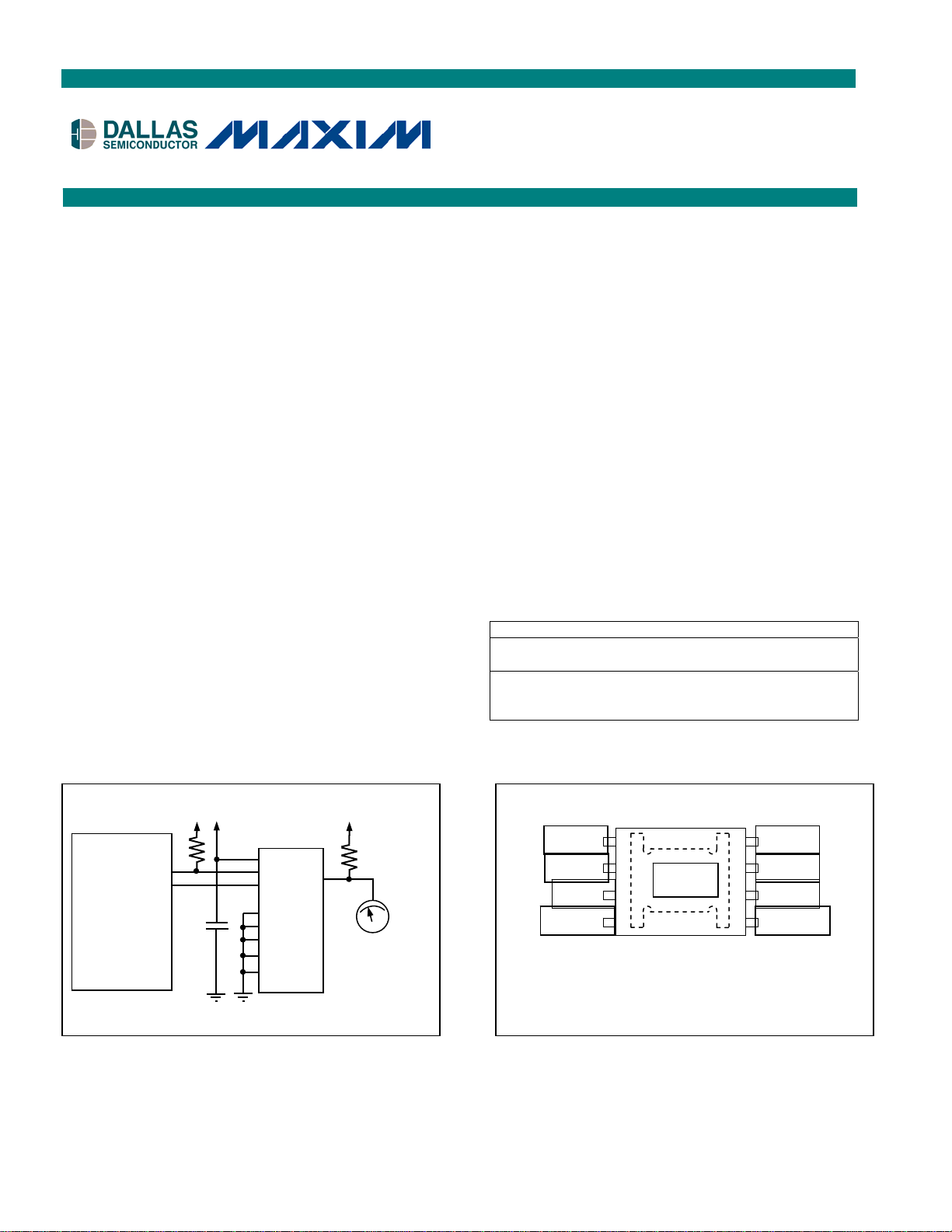
TYPICAL OPERATING CIRCUIT
DS620
0
1
2
1.7V to 3.5V
PO
Thermostat
1.7V to 3.5V
.
HOST
SDA
SCL
VDD
SDA
SCL
GND
PAD
DS620
Low-Voltage, ±0.5°C Accuracy
Digital Thermometer and Thermostat
FEATURES
Low-Voltage Operation: 1.7V to 3.5V
±0.5°C Accuracy from 0°C to +70°C
Operating Temperature Range: -55°C to +125°C
(-67°F to +257°F)
Temperature Measurements Require No
External Components
Resolution is User-Selectable to 10-, 11-, 12-, or
13-Bits (0.5°C, 0.25°C, 0.125°C, and 0.0625°C
LSb Weight, Respectively)
Multidroppable
Fast (200ms max) Temperature-to-Digital
Conversion Time
Thermostatic Settings are User-Definable and
Nonvolatile
Standalone Thermostat Capability
Data is Read/Written Through a 2-Wire Serial
Interface
Package: 8-Pin μSOP
ORDERING INFORMATION
PART TEMP RANGE PIN-PACKAGE
DS620U -55°C to +125°C
DS620U/T&R -55°C to +125°C
PIN CONFIGURATION
SD
SCL
PO
GND
8-Pin
μSOP Package
Exposed Pad
PAD
8 µSOP,
Exposed Pad
8 µSOP
Exposed Pad
Tape-and-Reel
VDD
0
1
2
1 of 15
041607
Page 2
DS620 Digital Thermometer and Thermostat
PIN DESCRIPTION
PIN NAME FUNCTION
1 SDA
2 SCL
3 PO
4 GND
5 A2
6 A1
7 A0
8 VDD
PAD
Figure 1. Block Diagram
DS620
SCL
SDA
Data Input/Output Pin for serial communication. Open drain. (No diode connection to VDD).
Clock Input Pin for 2-wire serial communication.
Programmable Output Pin. Open drain. (No diode connection to VDD).
Ground Pin.
Address Input Pin.
Address Input Pin. Also serves as an input to trigger one-shot conversions during standalone use.
Address Input Pin.
Supply Voltage Pin. +1.7V to +3.5V power supply pin.
PAD. Connect to GND or float. DO NOT CONNECT TO SUPPLY. The exposed pad is the best way to conduct
temperature into the package. Connecting PAD to a ground plane can assist in properly measuring the
temperature of the circuit board.
Temp. Core
Digital Control
Conversion Control
Address/Command
Decode
Address Counter
Memory Array
Configuration Register
TH, TL Registers
Digital Comparator
Temperature Register
Temperature Counter
User EEPROM Registers
Bandgap
ADC POR
2-Wire Interface
A2
A0
Memory Interface Logic
PO Pin
Control
Charge Pump
PO
A1
2 of 15
Page 3
DS620 Digital Thermometer and Thermostat
ABSOLUTE MAXIMUM RATINGS
Voltage Range on Any Pin, Relative to Ground -0.5V to +4.5V
Operating Temperature Range -55°C to +125°C
Storage Temperature Range
Soldering Temperature
-55°C to +125°C
See IPC/JEDEC J-STD-020A Specification
ESD rating on all pins 4KV HBM
Stresses beyond those listed under “Absolute Maximum Ratings” may cause permanent damage to the device. These are stress ratings only,
and functional operation of the device at these or any other conditions beyond those indicated in the operational sections of the specifications is
not implied. Exposure to the absolute maximum rating conditions for extended periods may affect device.
RECOMMENDED DC OPERATING CONDITIONS
(3.5V ≥ VDD ≥ 1.7V, TA = -55°C to +125°C.)
PARAMETER SYMBOL CONDITIONS MIN TYP MAX UNITS
Voltage Range on Any Pin,
Relative to Ground
Supply Voltage for EEPROM
Writes
(Note 1) 1.7 3.5 V
V
DD
(Note 1) 2.0 3.5 V
V
DD
DC ELECTRICAL CHARACTERISTICS
(3.5V ≥ VDD ≥ 1.7V, TA = -55°C to +125°C.)
PARAMETER SYMBOL CONDITIONS MIN TYP MAX UNITS
0°C to +70°C ±0.5
Thermometer Error T
Input Logic High VIH (Note 1)
Input Logic Low VIL (Note 1) - 0.5
SDA Output Logic Low Voltage
ERR
V
OL1
V
OL2
-55°C to +125°C ±2
0.7 x
V
DD
3mA sink current (Note 1) 0 0.4
6mA sink current (Note 1) 0 0.6
V
DD
0.5
0.3 x
V
DD
+
PO Saturation Voltage VOL 4mA sink current (Note 1) 0 0.4 V
Input Current for each I/O pin 0.4 < V
I/O Capacitance C
Standby Current I
10 pF
I/O
0°C to +70°C (Note 2) 2 µA
STBY
Temperature conversion, 55°C to +85°C (Note 3)
Active Supply Current IDD
Temperature conversion,
+85°C to +125°C (Note 3)
2
write (Note 3) 500 µA
E
< 0.9 x VDD -10 +10 µA
I/O
800
900
10 bit 25
Temperature Conversion Time TTC
11 bit 50
12 bit 100
13 bit 200
Note 1: All voltages are referenced to GND.
Note 2: Specified with SDA = V
Note 3: Specified with A
, A1, A2 = 0V or VDD.
0
; A0, A1, A2 = 0V or VDD.
DD
°C
V
V
V
µA
ms
3 of 15
Page 4

DS620 Digital Thermometer and Thermostat
AC ELECTRICAL CHARACTERISTICS
EEPROM AC Electrical Characteristics
PARAMETER SYMBOL CONDITIONS MIN TYP MAX UNITS
EEPROM Write Cycle Time TWR -40°C to +85°C 10 ms
-40°C ≤ TA ≤ +85°C
EEPROM Writes N
EEPROM Data Retention t
EEWR
EEDR
(Note 1)
T
= +25°C (Note 1) 40k 80k
A
-40°C to +125°C (Note 2) 10 years
2-Wire AC Electrical Characteristics
PARAMETER SYMBOL CONDITIONS MIN TYP MAX UNITS
SCL Frequency f
Bus Free Time Between a
STOP and START Condition
START and Repeat START
Hold Time from Falling SCL
Low Period of SCL t
High Period of SCL t
Repeated START Condition
Setup Time to Rising SCL
Data-Out Hold Time from
Falling SCL
Data-In Setup Time to Rising
SCL
0 400 KHz
SCL
t
1.3 µs
BUF
t
(Note 3, 4) 0.6 µs
HD:STA
(Note 3) 1.3 µs
LOW
(Note 3) 0.6 µs
HIGH
t
(Note 3) 0.6 µs
SU:STA
t
(Note 3) 0 0.9 µs
HD:DAT
(Note 3) 100 ns
t
SU:DAT
Rise Time of SDA and SCL tR (Note 3, 5)
Fall Time of SDA and SCL tF (Note 3, 5)
STOP Setup Time to Rising
SCL
Capacitive Load for Each BUS
Line
T
0.6 µs
SU:STO
C
400 pF
B
Input Capacitance CI 10 pF
Spike Pulse Width that can be
Suppressed by Input Filter
Note 1: V
Note 2: Write done at 25°C.
Note 3: All values referenced to 0.9 V
Note 4: After this period the first clock pulse is generated.
Note 5: For example, if C
must be 2.0V to 3.5V.
DD
= 300pF, then tR(MIN) = tF(MIN) = 50ns.
B
and 0.1 V
DD
0 50 ns
.
DD
10k 20k
20 +
0.1xC
20 +
0.1xC
B
B
1000 ns
300 ns
writes
4 of 15
Page 5
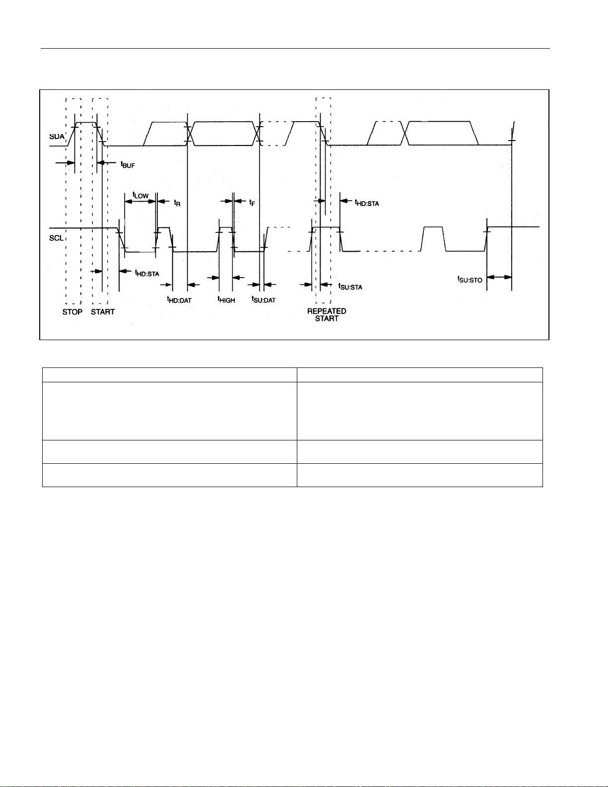
Figure 2. Timing Diagram
DS620 Digital Thermometer and Thermostat
Table 1. Register Summary
Parameter Information
TH and TL Registers
Size: 2-Bytes
Note that the 3 LSbs are always “don’t cares” for writes
(i.e., they are not saved) and always read out as 0s.
Configuration Register
Size: 2-Bytes
Temperature Register
Size: 2-Bytes
EEPROM
Factory State:
TH = 15ºC (0000 0111 1000 0000) [0780h]
TL = 10ºC (0000 0101 0000 0000) [0500h]
SRAM and EEPROM. See Figure 4 and Table 5 for
detailed information and power-up/factory state.
SRAM Power-Up State: -60ºC
(1110 0010 0000 0000) [E200h]
TEMPERATURE MEASUREMENT
The DS620 measures temperature using a bandgap-based temperature sensor. A delta-sigma, analog-to-digital
converter (ADC) converts measured temperature to a 10-, 11-, 12-, or 13-bit (user-selectable) digital value that is
calibrated in °C; for °F applications, a lookup table or conversion routine must be used. Throughout this data sheet,
the term “conversion” is used to refer to the entire temperature measurement and ADC sequence.
The DS620 can be configured to power up either automatically converting temperature or in a low-power standby
state. The preferred power-up mode can be set using the AUTOC bit in the configuration register as explained in
the Configuration Register section of this data sheet.
The DS620 can be programmed to perform continuous consecutive conversions (continuous conversion mode) or
to perform single conversions on command (one-shot mode). The conversion mode is programmed through the
1SHOT bit in the configuration register as explained in the Configuration Register section of this data sheet. In
continuous conversion mode, conversions are performed after a Start Convert command is issued (or upon powerup if the AUTOC bit in the configuration register is set to 1) until a Stop Convert command is issued, at which time
the device goes into a low-power standby state. Continuous conversions can be restarted at any time using the
Start Convert command. In one-shot mode, the DS620 performs a single temperature conversion either at powerup (if AUTOC = 1) or when a Start Convert command is issued (if AUTOC = 0). When the conversion is complete,
5 of 15
Page 6

DS620 Digital Thermometer and Thermostat
the device enters a low-power standby state and remains in that state until a temperature conversion is again
initiated by a Start Convert command.
The R0 and R1 bits in the configuration register allow the user to set the conversion resolution to be 10, 11, 12, or
13 bits (0.5°C, 0.25°C, 0.125°C, and 0.0625°C LSb weight, respectively) as shown in Table 6. The default
resolution at power-up is 13-bits. Note that the conversion time doubles for each additional bit of resolution.
After each conversion, the digital temperature is stored as a 16-bit two’s complement number in the 2-byte
temperature register as shown in Figure 3. The temperature register is located in address spaces AAh (MSB) and
ABh (LSB) of the DS620 memory. The sign bit (S) indicates if the temperature is positive (S = 0) or negative (S =
1). Bits 2, 1, and 0 of the temperature register are hardwired to 0. When the device is configured for 13-bit
resolution, the 13 MSbs (bits 15 through 3) of the temperature register will contain temperature data. For 12-bit
resolution, the 12 MSbs (bits 15 through 4) of the temperature register will contain data, and bit 3 will be 0.
Likewise, for 11-bit resolution, the 11 MSbs (bits 15 through 5) will contain data, and for 10-bit the 10 MSbs (bits 15
through 6) will contain data, and all unused LSbs will contain 0s. Table 2 gives examples of 13-bit resolution output
data and the corresponding temperatures.
Figure 3. Temperature, TH, And TL Register Format
MS Byte
LS Byte
bit 15 bit 14 bit 13 Bit 12 bit 11 bit 10 bit 9 bit 8
S 2
bit 7 bit 6 bit 5 Bit 4 bit 3 bit 2 bit 1 bit 0
0
2
2
7
2
-1
2
6
2
-2
2
5
2
-3
2
4
2
-4
0 0 0
3
2
2
2
1
Table 2. 13-Bit Resolution Temperature/Data Relationship
Temperature (°C)
+125 0011 1110 1000 0000 3E80h
+25.0625 0000 1100 1000 1000 0C88h
+10.125 0000 0101 0001 0000 0510h
+0.5 0000 0000 0100 0000 0040h
0 0000 0000 0000 0000 0000h
-0.5 1111 1111 1100 0000 FFC0h
-10.125 1111 1010 1111 0000 FAF0h
-25.0625 1111 0011 0111 1000 F378h
-55 1110 0100 1000 0000 E480h
Digital Output (binary) Digital Output (hex)
WRITING TO THE TEMPERATURE REGISTER
The user is given access to write to the DS620 temperature register. This feature can be used for system test and
debugging by allowing the user to force the temperature reading above or below fault thresholds without having to
heat or cool the device.
If data is written to the temperature register while conversions are in progress, the result of the next completed
conversion will overwrite any data that was written to the temperature register. Additionally, no update of the flag
bits in the configuration register, nor an update of the PO pin occur as a result of the temperature being written if a
conversion is taking place. To avoid this from happening, conversions should first be stopped before writing to the
temperature register. When writing to the temperature register, both the MSB and the LSB should be written. An
update of the flag bits and PO pin will only occur after the LSB has been written. See Writing to the DS620 for more
information.
6 of 15
Page 7

DS620 Digital Thermometer and Thermostat
g
g
THERMOSTAT OPERATION
The PO pin on the DS620 operates as the thermostat output when it is configured as PO
P01 and P02 bits of the configuration register. In both of these configurations, PO is updated after every
temperature conversion or write to the temperature register, and remains at the updated value until the next
conversion or write completes. PO
user-defined upper and lower trip-points. PO
-HIGH
and PO
-HIGH
the value stored in the upper trip-point register (T
value stored in the lower trip-point register (T
hysteresis into the output response. Similarly, PO
below the value stored in the low trip-point register (T
the value stored in the upper trip-point register (T
A0h (MSB) and A1h (LSB) and the T
register is located in address spaces A2h (MSB) and A3h (LSB) of the
L
are active-low and are activated and deactivated based on
-LOW
is activated when the measured temperature meets or exceeds
), and stays active until the temperature meets or falls below the
H
) (see Figure 4a). This allows the user to program any amount of
L
is activated when the measured temperature meets or goes
-LOW
), and stays active until the temperature meets or exceeds
L
) (see Figure 4b). The TH register is located in address spaces
H
DS620 memory.
-HIGH
or PO
through the
-LOW
The T
and TL registers (see Table 1) contain centigrade temperature values in two’s complement format and are
H
stored in EEPROM; therefore, they are nonvolatile (NV) and can be programmed prior to installation of the DS620
for use in standalone applications. All bits in the T
and TL registers are used in the comparison to the temperature
H
value in the temperature register for the thermostat operation, regardless of the number of bits used for the
temperature conversions as decided by the R0 and R1 bits in the configuration register. Therefore, to ensure
proper thermostat operation, any bits not used for the temperature measurement should be set to 0 in the T
T
registers. For example, for 11-bit temperature conversions, bits 3 and 4 in the TH and TL register should be set to
L
0 prior to comparison to the measured temperature. (Bits 0 to 2 are automatically set to 0).
Another thermostat feature is the temperature high and low flags (THF and TLF) in the configuration register.
These bits provide a record of whether the temperature has ever been equal to or greater than T
less than T
exceeds the T
meets or falls below the T
at anytime since power up or since the bits were last cleared. If the temperature ever meets or
L
register value, the THF bit in the configuration register is set to 1, and if the temperature ever
H
value, the TLF bit in the configuration register is set to 1. Once THF or TLF has been
L
or equal to or
H
set, it remains set until the power is cycled or it is overwritten with a 0 by the user.
Figure 4. Thermostat Operation
a) PO-high
ic 1
Lo
Logic 0
TL
Tem
Temp
T
H
b) PO-low
Lo
ic 1
Logic 0
Tem
T
L
TH
Temp
STANDALONE THERMOSTAT OPERATION
The DS620 can function as a standalone thermostat, i.e., it can provide thermostat functionality without requiring
communication with a microcontroller. For standalone thermostat operation, the T
must be programmed to the desired values prior to installation. For standalone operation, the AUTOC bit in the
configuration register must be set to 1 so that measurements begins automatically at power up. This also
configures the A1 pin as an input pin that can trigger a conversion. In addition, PO must be configured as PO
or PO
. The 1SHOT bit in the configuration register is used to enable the DS620 to perform continuous
-LOW
conversions at power up (1SHOT = 0) or a single conversion (one-shot) at power up or upon request (1SHOT = 1).
In one-shot mode, one conversion is performed at power-up and then the device enters a low-power standby state
until A1 is toggled high. The A1 pin must be toggled low and back high again to start another conversion.
, TL, and configuration registers
H
and
H
-HIGH
7 of 15
Page 8

DS620 Digital Thermometer and Thermostat
PO PIN
The PO pin is a user-programmable open-drain output, which is configured through the PO1 and PO2 bits in the
configuration register. PO can operate as a thermostat output (PO
of peripheral devices. When PO is configured as PO
Thermostat Operation section. This pin can be reconfigured at anytime to switch between functions. Table 3
defines the various configuration options for this pin.
-HIGH
or PO
-HIGH
or PO
, this pin operates as described in the
-LOW
), or it can be forced low for control
-LOW
Table 3. PO Configuration
Function PO2 PO1
Thermostat Output (PO-high) 1 1
Thermostat Output (PO-low) 1 0
Force PO Low 0 X
EEPROM REGISTERS AND MEMORY MAP
The DS620 has a 14-byte linear address space with registers for temperature, thermostat thresholds, and control
as well as four bytes of user EEPROM for general use. All address space is shadowed by RAM. The DS620
Memory Map is shown in Table 4.
See the Writing to the DS620 and the Reading from the DS620 sections for details in writing to and reading from
the DS620 EEPROM registers and memory map.
Table 4. Memory Map
Address (hex) Description
A0 TH MSB
A1 TH LSB
A2 TL MSB
A3 TL LSB
A4 User
A5 User
A6 User
A7 User
A8 Undefined
A9 Undefined
AA Temperature MSB
AB Temperature LSB
AC Configuration MSB
AD Configuration LSB
CONFIGURATION REGISTER
The configuration register allows the user to program various DS620 options such as conversion resolution,
operating mode, and thermostat capability. It also provides information to the user about conversion status,
EEPROM activity, device address, and thermostat activity. The configuration register is arranged as shown in
Figure 5 and detailed descriptions of each bit are provided in Table 5. It is located in address spaces ACh (MSB)
and ADh (LSB) in the DS620 memory. Note that the R0, R1, AUTOC, 1SHOT, and PO1 bits are stored in
EEPROM so they can be programmed prior to installation if desired. All other configuration bits are SRAM and
power up in the state shown in Table 5.
8 of 15
Page 9

DS620 Digital Thermometer and Thermostat
Figure 5. Configuration Register
MS Byte
LS Byte
*
Stored in EEPROM
Table 5. Configuration Register Bit Descriptions
Bit Name User Access Functional Description
DONE
NVB
THF
TLF
*
R1
*
R0
AUTOC
1SHOT
*
*
bit 15 bit 14 bit 13 bit 12 bit 11 bit 10 bit 9 bit 8
Address ACh
DONE NVB THF TLF R1* R0* AUTOC
bit 7 bit 6 bit 5 bit 4 bit 3 bit 2 bit 1 bit 0
PO2 PO1
*
Address ADh
A2 A1 A0 M* M* M*
At power-up, DONE = 1. (Unless AUTOC = 1)
Read Only
DONE = 0—Temperature conversion is in progress.
DONE = 1—Temperature conversion is complete.
Read Only
At power-up, NVB = 0
NVB = 1—Write to an E
2
memory cell is in progress
NVB = 0—Nonvolatile memory is not busy.
At power-up, THF = 0
THF = 1—The measured temperature has reached or exceeded the value
Read/Write
stored in the T
register at anytime since power-up or since the bit was last
H
cleared. THF remains a 1 until the power is cycled or it is overwritten with a
0 by the user.
At power-up, TLF = 0
TLF = 1—The measured temperature has met or fallen below the value
Read/Write
stored in the T
register at anytime since power-up or since the bit was last
L
cleared. TLF remains a 1 until the power is cycled or it is overwritten with a
0 by the user.
Read/Write
Read/Write
Used to set conversion resolution (see Table 6).
Factory state = 1
Used to set conversion resolution (see Table 6).
Factory state = 1
Determines whether the DS620 powers up idle or converting.
Read/Write
Factory state = 0
AUTOC = 1—DS620 powers-up converting temperature.
AUTOC = 0—DS620 powers-up idle.
Configures temperature conversion mode. Factory state = 0
1SHOT = 1: One-shot mode
For AUTOC = 0, the device powers up idle The Start Convert
command causes a single temperature conversion and then the
device returns to a low-power standby state.
If AUTOC = 1, the A1 pin is reconfigured as a conversion trigger for
standalone operation and the device powers up and performs 1
Read/Write
conversion. Single conversions can be initiated using the Start
Convert command or by toggling A1 high.
1SHOT = 0: Continuous conversion mode
For AUTOC = 0, the Start Convert command initiates continuous
conversions.
For AUTOC = 1, the device powers up performing continuous
conversions. Note: Changing the 1SHOT bit to 1 while continuous
conversions are in progress does not stop the conversions. A Stop
Convert command must first be issued after which one-shot
*
1SHOT*
9 of 15
Page 10

DS620 Digital Thermometer and Thermostat
conversions can be performed.
See Writing the 1SHOT Bit Command Sequence section for writing more
information on writing the 1SHOT bit.
At power-up, PO2 = 1.
PO2
Read/Write
PO2 = 0 forces the PO pin low (see Table 3)
PO2 = 1 configures PO as the thermostat output (PO
-HIGH
or PO
-LOW
, as
determined by PO1).
PO1*
Read/Write
When PO2 = 1, PO1 configures the PO pin as either PO
Table 3)
When PO2 = 0, PO1 is a “don’t care”.
-HIGH
or PO
-LOW
(see
Factory state = 0
A2 Read Only Shows address bit A2, as determined by pin A2.
A1 Read Only Shows address bit A1, as determined by pin A1.
A0 Read Only Shows address bit A0, as determined by pin A0.
M* Read/Write User memory for general-purpose data storage.
*
Stored in EEPROM
Table 6. Resolution Configuration
R1 R0 Resolution LSb Weight (°C)
0 0 10-bit 0.5 25
0 1 11-bit 0.25 50
1 0 12-bit 0.125 100
1 1 13-bit 0.0625 200
Max Conversion
Time (ms)
2-WIRE SERIAL DATA BUS
The DS620 communicates over a standard bidirectional 2-wire serial data bus that consists of a serial clock (SCL)
signal and serial data (SDA) signal. The DS620 interfaces to the bus through the SCL input pin and open-drain
SDA I/O pin. All communication is MSb first.
The following terminology is used to describe 2-wire communication:
Master Device: Microprocessor/microcontroller that controls the slave devices on the bus. The master device
generates the SCL signal and START and STOP conditions.
Slave: All devices on the bus other than the master. The DS620 always functions as a slave.
Bus Idle or Not Busy: Both SDA and SCL remain high. SDA is held high by a pullup resistor when the bus is idle,
and SCL must either be forced high by the master (if the SCL output is push-pull) or pulled high by a pullup resistor
(if the SCL output is open-drain).
Transmitter: A device (master or slave) that is sending data on the bus.
Receiver: A device (master or slave) that is receiving data from the bus.
START Condition: Signal generated by the master to indicate the beginning of a data transfer on the bus. The
master generates a START condition by pulling SDA from high to low while SCL is high (see Figure 6). A
“repeated” START is sometimes used at the end of a data transfer (instead of a STOP) to indicate that the master
will perform another operation.
STOP Condition: Signal generated by the master to indicate the end of a data transfer on the bus. The master
generates a STOP condition by transitioning SDA from low to high while SCL is high (see Figure 6). After the
STOP is issued, the master releases the bus to its idle state.
Acknowledge (ACK): When a device (either master or slave) is acting as a receiver, it must generate an
acknowledge (ACK) on the SDA line after receiving every byte of data. The receiving device performs an ACK by
pulling the SDA line low for an entire SCL period (see Figure 6). During the ACK clock cycle, the transmitting
device must release SDA. A variation on the ACK signal is the “not acknowledge” (NACK). When the master device
10 of 15
Page 11

DS620 Digital Thermometer and Thermostat
is acting as a receiver, it uses a NACK instead of an ACK after the last data byte to indicate that it is finished
receiving data. The master indicates a NACK by leaving the SDA line high during the ACK clock cycle.
Slave Address: Every slave device on the bus has a unique 7-bit address that allows the master to access that
device. The DS620’s 7-bit bus address is 1 0 0 1 A
corresponding input pins. The three address pins allow up to eight DS620s to be multidropped on the same bus.
Control Byte: The control byte is transmitted by the master and consists of the 7-bit slave address plus a
read/write (R/W¯¯) bit (see Figure 7). If the master is going to read data from the slave device then R/W¯¯ = 1, and if
the master is going to write data to the slave device then R/W¯¯ = 0.
Address Byte: The address byte is used by the master to tell the DS620 which address location in the memory
map in Table 4 is going to be accessed during communication or which command should be performed. See
Command Set section.
2 A1 A0
, where A2, A1, and A0 are user-selectable via the
Figure 6. START, STOP, AND ACK SIGNALS
SDA
SCL
START
Condition
ACK (or NACK)
From Receiver
STOP
Condition
Figure 7. Control Byte
bit 7 bit 6 bit 5 bit 4 bit 3 bit 2 bit 1 bit 0
1 0 0 1 A2 A
A
1
0
R/W¯¯
GENERAL 2-WIRE INFORMATION
All data is transmitted MSb first over the 2-wire bus.
One bit of data is transmitted on the 2-wire bus each SCL period.
A pullup resistor is required on the SDA line and, when the bus is idle, both SDA and SCL must remain in a logic-
high state.
All bus communication must be initiated with a START condition and terminated with a STOP condition. During a
START or STOP is the only time SDA is allowed to change states while SCL is high. At all other times, changes
on the SDA line can only occur when SCL is low: SDA must remain stable when SCL is high.
After every 8-bit (1-byte) transfer, the receiving device must answer with an ACK (or NACK), which takes one
SCL period. Therefore, nine clocks are required for every one-byte data transfer.
INITIATING 2-WIRE COMMUNICATION
To initiate 2-wire communication, the master generates a START followed by a control byte containing the DS620
slave address. The R/W bit of the control byte must be a 0 (write) since the master next writes a command byte or
an address byte. The DS620 responds with an ACK after receiving the control byte. This must be followed by a
command byte from the master which indicates what type of command operation is to be performed, or an address
byte when the master intends to write to or read from the DS620. The DS620 again responds with an ACK after
receiving the command or address byte. The master can then issue a STOP to signal the end of the
communication sequence, or continue writing to the address memory. See the Command Set section for details on
11 of 15
Page 12

DS620 Digital Thermometer and Thermostat
the DS620 commands. See Writing to the DS620 or Reading from the DS620 for more information on reading from
and writing to the DS620.
WRITING TO THE DS620
The master can write data to the DS620 by issuing an address byte following the control byte. The R/W bit in the
control byte must be a 0 (write). After receiving an ACK from the DS620 in response to the control byte, the master
sends the address of the first register byte to be written, loading the address counter with the desired location. The
DS620 responds with another ACK, after which the master sends the data to be written. After receiving each byte
of data, the DS620 responds with an ACK. The master continues to write data to successive address locations until
it indicates there is no more data to be written by sending a STOP or repeated START condition. The DS620
ignores any data written once the address increments past ADh, the last defined register in the DS620 memory,
and indicates this by sending a NACK after each byte. It also ignores data written to undefined addresses A8h and
A9h. All writes to the DS620 are made to the shadow RAM. Once data is written to the shadow RAM, it is only
stored to EEPROM by issuance of a Copy Data command from the master. At that time all registers are copied to
EEPROM, except the Temperature registers, which are SRAM only, and the undefined registers. The DS620 must
be set to the continuous conversion mode and be actively converting temperature to enable the Copy Data
command to function properly. See Copying to EEPROM Command Sequence for more information.
READING FROM THE DS620
The master can read data from the DS620 by issuing an address byte following the control byte. The R/W bit in the
control byte must be a 0 (write). After receiving an ACK from the DS620 in response to the control byte, the master
writes the address of the first register byte to be read, loading the address counter with the desired location. The
DS620 will respond with another ACK. The master then must issue a repeated START (or a STOP and a START)
followed by a control byte with the same slave address as the first control byte. However, this time the R/W bit must
be a 1 which tells the DS620 that a “read” is being performed. After the DS620 sends an ACK in response to this
control byte, it begins transmitting the requested data on the next clock cycle. The master responds with an ACK
between each byte of data read from the DS620 until no further bytes of data are to be read, at which time the
master responds with a NACK followed by a STOP. The DS620 sends all 1’s (FFh) once the address increments
past ADh, the last defined register in the DS620 memory. There is no guaranteed state of data read from the
undefined registers, A8h and A9h. The Recall Data command should be issued before a read to assure that the
contents of the EEPROM will be in the Shadow RAM when read.
COMMAND SET
The DS620 command set is detailed below:
Start Convert [ 51h ] 0101 0001
Initiates temperature conversions. If the part is in one-shot mode (1SHOT = 1), only one conversion is performed.
In continuous mode (1SHOT = 0), continuous temperature conversions are performed until a Stop Convert
command is issued (even if 1SHOT is changed to a 1).
Stop Convert [ 22h ] 0010 0010
Stops temperature conversions when the device is in continuous conversion mode (1SHOT = 0). This command
has no function if the device is in one-shot mode (1SHOT = 1)
Recall Data [ B8h ] 1011 1000
Refreshes SRAM shadow register with EEPROM data.
Copy Data [ 48h ] 0100 1 000
Copies data from all SRAM shadow registers to EEPROM.
NOTE: The DS620 must be set to the continuous conversion mode and be actively converting temperature to
enable the Copy Data command to function properly. See example command sequence in the Copying to
EEPROM Command Sequence section for more information.
Software POR [ 54h ] 0101 0100
Initiates a software power-on-reset (POR), which stops temperature conversions and resets all registers and logic
to their power-up states. The software POR allows the user to simulate cycling the power without actually powering
down the device. This command should not be issued while a Copy Data command is in progress.
12 of 15
Page 13

DS620 Digital Thermometer and Thermostat
COPYING TO EEPROM COMMAND SEQUENCE
Data is written to DS620 and then copied from SRAM to EEPROM
BUS
MASTER
MODE
TX RX START Bus master initiates a START condition. 1
TX RX <address, 0>
RX TX ACK
TX RX A4h
RX TX ACK DS620 generates acknowledge. 5
TX RX <data>
RX TX ACK DS620 generates acknowledge. 7
TX RX <data>
RX TX ACK DS620 generates acknowledge. 9
TX RX <data>
RX TX ACK DS620 generates acknowledge. 11
TX RX <data>
RX TX ACK DS620 generates acknowledge. 13
TX RX START Bus master generates a repeated start condition. 14
TX RX <address, 0>
RX TX ACK DS620 generates acknowledge. 16
TX RX ACh
RX TX ACK DS620 generates acknowledge. 18
TX RX xxxxxxx0b
RX TX ACK DS620 generates acknowledge. 20
TX RX START Bus master generates a repeated start condition. 21
TX RX <address, 0>
RX TX ACK DS620 generates acknowledge 23
TX RX 51h
RX TX ACK
TX RX START Bus master generates a repeated start condition. 26
TX RX <address, 0>
RX TX ACK DS620 generates acknowledge. 28
TX RX ACh
DS620
MODE
DATA
(MSB
FIRST)
COMMENTS
Bus master sends DS620 address, R/W = 0.
DS620 generates acknowledge bit. 3
Bus master sends the address location of the first byte
of data to be written. (In this case the first byte of user
EEPROM).
Bus master sends one byte of data to the SRAM
location for EEPROM address A4h.
Bus master sends one byte of data to the SRAM
location for EEPROM for address A5h.
Bus master sends one byte of data to the SRAM
location for EEPROM for address A6h.
Bus master sends one byte of data to the SRAM
location for EEPROM for address A7h.
Bus master sends DS620 address, R/W = 0.
Bus master sends the address location of the MSb of
the configuration register (contains the 1SHOT bit).
This writes to the SRAM location corresponding the
EEPROM location. NOTE: Sequence numbers 17
through 23 need to be done only if DS620 is in 1SHOT
mode: 1SHOT = 1.
Bus master writes to the configuration register putting
the DS620 in continuous conversion mode: 1SHOT =
0.
Bus master sends DS620 address, R/W = 0.
Master sends START CONVERT command to DS620
to start temperature conversions.
DS620 generates acknowledge bit and begins
conversions.
Bus master sends DS620 address, R/W = 0.
Bus master sends the address location of the MSb of
the configuration register (contains the 1SHOT bit).
This writes to the SRAM location corresponding the
EEPROM location. NOTE: command sequence
numbers 29 through 34 need only be done if a return to
1SHOT mode operation is needed.
SEQUENCE
NUMBER
2
4
6
8
10
12
15
17
19
22
24
25
27
29
13 of 15
Page 14

DS620 Digital Thermometer and Thermostat
RX TX ACK DS620 generates acknowledge. 30
TX RX xxxxxxx1b
TX RX START Bus master generates a repeated start condition. 32
TX RX <address, 0>
RX TX ACK DS620 generates acknowledge. 34
TX RX 48h
RX TX ACK DS620 generates acknowledge. 36
TX RX START Bus master generates a repeated start condition. 37
TX RX <address, 0>
RX TX ACK DS620 generates acknowledge. 39
TX RX 22h
RX TX ACK DS620 generates acknowledge. 41
TX RX STOP
Bus master writes to the configuration register putting
the DS620 back in 1SHOT mode: 1SHOT = 1.
Bus master sends DS620 address, R/W = 0.
Master sends COPY DATA command to DS620 to
copy data in from SRAM memory to EEPROM memory.
Bus master sends DS620 address, R/W = 0.
Bus master sends a STOP CONVERT command to
stop the DS620 from continuously converting
temperature. NOTE: Bus master should ensure that
EEPROM copy operation is complete before executing
the STOP CONVERT command by either waiting 10ms
from the time of the COPY DATA command or
checking the NVB bit in configuration register
Bus master sends STOP condition to end
communication with DS620. (The bus master could
send a repeated start condition if additional
communication with the DS620 is desired.)
WRITING THE 1SHOT BIT COMMAND SEQUENCE
Configuring from continuous mode to 1SHOT mode.
BUS
MASTER
MODE
TX RX START Bus master initiates a START condition. 1
TX RX <address, 0>
RX TX ACK DS620 generates acknowledge bit. 3
TX RX 51h
RX TX ACK
TX RX START Bus master generates a repeated start condition. 6
TX RX <address, 0>
RX TX ACK DS620 generates acknowledge. 8
TX RX ACh
RX TX ACK DS620 generates acknowledge. 10
TX RX xxxxxxx1b
RX TX ACK DS620 generates acknowledge. 12
TX RX START Bus master generates a repeated start condition. 13
TX RX <address, 0>
RX TX ACK DS620 generates acknowledge. 15
TX RX 48h
DS620
MODE
DATA
(MSB FIRST)
COMMENTS
Bus master sends DS620 address, R/W = 0.
Master sends START CONVERT command to DS620
to start temperature conversions.
DS620 generates acknowledge bit and begins
conversions.
Bus master sends DS620 address, R/W = 0.
Bus master sends the address location of the MSb of
the configuration register (contains the 1SHOT bit).
This writes to the SRAM location corresponding the
EEPROM location.
Bus master writes to the configuration register putting
the DS620 in 1SHOT mode: 1SHOT = 1.
Bus master sends DS620 address, R/W = 0.
Master sends COPY DATA command to DS620 to
copy data in from SRAM memory to EEPROM
memory.
31
33
35
38
40
42
SEQUENCE
NUMBER
2
4
5
7
9
11
14
16
14 of 15
Page 15

DS620 Digital Thermometer and Thermostat
RX TX ACK DS620 generates acknowledge. 17
TX RX START Bus master generates a repeated start condition. 18
TX RX <address, 0>
RX TX ACK DS620 generates acknowledge. 20
TX RX 22h
RX TX ACK DS620 generates acknowledge. 22
TX RX STOP
Configuring from 1SHOT to mode to continuous conversion mode.
BUS
MASTER
MODE
TX RX START Bus master initiates a START condition. 1
TX RX <address, 0>
RX TX ACK DS620 generates acknowledge bit. 3
TX RX ACh
RX TX ACK DS620 generates acknowledge. 5
TX RX xxxxxxx0b
RX TX ACK DS620 generates acknowledge. 7
TX RX START Bus master generates a repeated start condition. 8
TX RX <address, 0>
RX TX ACK DS620 generates acknowledge. 10
TX RX 51h
RX TX ACK
TX RX START Bus master generates a repeated start condition. 13
TX RX <address, 0>
RX TX ACK DS620 generates acknowledge. 15
TX RX 48h
RX TX ACK DS620 generates acknowledge. 17
TX RX STOP
DS620
MODE
DATA
(MSB
FIRST)
Bus master sends DS620 address, R/W = 0.
Bus master sends STOP CONVERT command to
stop the DS620 from continuously converting
temperature. NOTE: Bus master should ensure that
EEPROM copy operation is complete before
executing the STOP CONVERT command by either
waiting 10ms from the time of the COPY DATA
command or checking the NVB bit in configuration
register
Bus master sends STOP condition to end
communication with DS620. (The bus master could
send a repeated start condition if additional
communication with the DS620 is desired.)
COMMENTS
Bus master sends DS620 address, R/W = 0.
Bus master sends the address location of the MSb of
the configuration register (contains the 1SHOT bit).
This writes to the SRAM location corresponding the
EEPROM location.
Bus master writes to the configuration register putting
the DS620 in continuous conversion mode: 1SHOT =
0.
Bus master sends DS620 address, R/W = 0.
Master sends START CONVERT command to DS620
to start temperature conversions.
DS620 generates acknowledge bit and begins
conversions.
Bus master sends DS620 address, R/W = 0.
Master sends COPY DATA command to DS620 to
copy data in from SRAM memory to EEPROM
memory.
Bus master sends STOP condition to end
communication with DS620. (The bus master could
send a repeated start condition if additional
communication with the DS620 is desired.)
19
21
23
SEQUENCE
NUMBER
2
4
6
9
11
12
14
16
18
15 of 15
 Loading...