Page 1

General Description
The DS5250 is a highly secure, four clocks-permachine cycle, 100% 8051-instruction-set-compatible
microprocessor in Maxim’s secure microcontroller family.It was designed to be the cryptographic engine of
PIN pads, financial terminals, and any other application
in which data security is paramount. A key feature of
the device is that it encrypts its program memory and
optionally its data memory with a hardware-based single- or triple-DES (data encryption standard) algorithm,
making it almost impossible to extract information. It
also implements block cipher encoding that uses block
addresses to modify the encrypted data, further
strengthening security. This makes the device ideal for
storage and transmission of passwords, personal identification numbers, encryption keys, and other highly
confidential information.
Applications
PIN Pads
Financial Terminals
Data Security Applications
Features
♦ Feature-Rich, 8051-Compatible Microprocessor
Accesses Up to 4MB Program and 4MB Data
Memory (All Nonvolatile)
In-System Programmable Through Serial Port
In-Application Programmable Through User Software
Allows Self-Modification of Program/Data Memory
Four 8-Bit Ports/One 6-Bit Port
Three 16-Bit Timer/Counters
256 Bytes of Scratchpad RAM
♦ Advanced Features
CRC-16/32 Generator
5KB Internal SRAM (Optional 1KB Stack)
Single or 3DES Engine
Partitionable Memory Segments Variable from 4KB to
256KB
♦ High-Speed Architecture
Four Clocks-per-Machine Cycle
DC-to-25MHz Operation
Single-Cycle Instruction in 160ns
Dual Data Pointers Can Increment or Decrement
Independently
Automatic Data Pointer (DPTR) Selection Available
Programmable Speed MOVX Instructions
1KB On-Chip Instruction Cache
♦ High-Reliability Operation
Power-Fail/Overvoltage Reset
Early-Warning Power-Fail Interrupt
Watchdog Timer
♦ Nonvolatile Functions
On-Chip Real-Time Clock with Alarm Interrupt
2KB Battery-Backed Internal SRAM
♦ Interrupts
15 Interrupts with Seven External Sources
♦ Security Features
Executes Single/3DES-Encrypted Programs to
Prevent Observation
Two Self-Destruct Inputs
4096-Bit Modulo-Arithmetic Accelerator (MAA) for
Public/Private Key Operations
Tamper Sensors Detect Thermal/Voltage/Probe Attacks
Programmable Attack Countermeasures
Secure-Loader Mode
True Random-Number Generator (RNG)
Unique ID Number in Every Device
Separate Program/Data Cryptograph
Program Memory Integrity Checking
♦ Evaluation Kit Available (DS5250-KIT)
DS5250
High-Speed Secure Microcontroller
________________________________________________________________
Maxim Integrated Products
1
Ordering Information
Rev 4; 11/08
For pricing, delivery, and ordering information, please contact Maxim Direct at 1-888-629-4642,
or visit Maxim’s website at www.maxim-ic.com.
Note: Some revisions of this device may incorporate deviations from published specifications known as errata. Multiple revisions of any device may be
simultaneously available through various sales channels. For information about device errata, contact the factory.
ABRIDGED DATA SHEET
EVALUATION KIT
AVAILABLE
PART TEMP RANGE PIN-PACKAGE
DS5250F-825 0°C to +70°C 80 MQFP
DS5250F-825+ 0°C to +70°C 80 MQFP
DS5250F-8N5 -40°C to +85°C 80 MQFP
DS5250F-8N5+ -40°C to +85°C 80 MQFP
DS5250F-125 0°C to +70°C 100 MQFP
DS5250F-125+ 0°C to +70°C 100 MQFP
DS5250F-1N5 -40°C to +85°C 100 MQFP
DS5250F-1N5+ -40°C to +85°C 100 MQFP
Pin Configurations and Selector Guide appear at end of
data sheet.
+
Denotes a lead-free/RoHS-compliant package.
Page 2

DS5250
High-Speed Secure Microcontroller
10 ______________________________________________________________________________________
ABRIDGED DATA SHEET
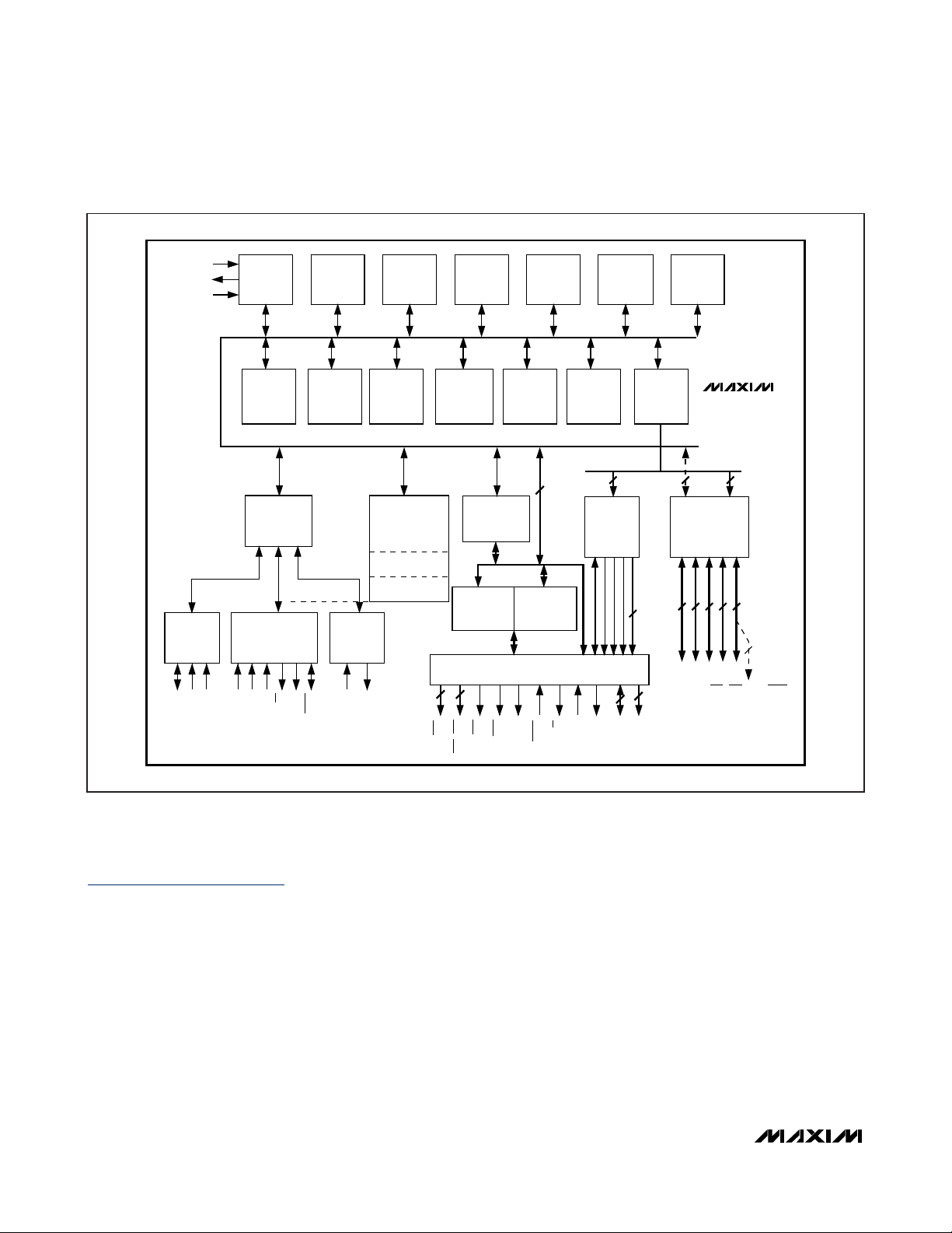
Figure 4. Block Diagram
Note to readers: This document is an abridged version of the full data sheet. To request the full data sheet, go to
www.maxim-ic.com/DS5250 and click on Request Full Data Sheet.
RTCX1
RTCX2
GND2
RESET
RST
SDI1
SDI2
REAL-TIME
CLOCK
RANDOM-
NUMBER
GENERATOR
WATCHDOG
AND POWER
CONTROL
POWER AND
TEMPERATURE
MONITOR
CC
BAT
V
GND
V
PF
REGISTERS
CC0
V
SERIAL
PORTS
0, 1
INTERNAL
CLOCKS
VRST
STACK
POINTER
INSTRUCTION
CPU
INTERNAL CONTROL/DATA BUS
INTERNAL
SRAM
3KB x 8
1KB x 8
1KB x 8
XTAL1
XTAL2
USER
DES
ENGINE
DECODER
AND
CONTROLS
INSTRUCTION
CACHE
PROGRAM
MEMORY
CRYPTOGRAPH
BYTE-WIDE BUS INTERFACE
CEx
FOE
PE1, PE2
MODULO-
ARITHMETIC
CRC
GENERATOR
8
DATA
MEMORY
CRYPTOGRAPH
PPH
FWP
V
ACCEL.
INTERRUPT
LOGIC
INTERNAL ADDRESS BUS
24
MMU
ALE
R/W
MSEL
PROG
TIMERS
0, 1, 2
8
BDx
PC AND
DPTRs
21
BAx
ROM
LOADER
8
I/O PORTS
P0
P1 P2 P3 P4
DS5250
8
8
888821
8
PE3, PE4, AND CExN
 Loading...