

Page 1
CE2
PE2
W
PE3
PE4
CE3 CE4
PF
V
G
P
1
C
1
C
BD4
www.maxim-ic.com
DS5002FP
Secure Microprocessor Chip
GENERAL DESCRIPTION
The DS5002FP secure microprocessor chip is a
secure version of the DS5001FP 128k soft
microprocessor chip. In addition to the memory and
I/O enhancements of the DS5001FP, the secure
microprocessor chip incorporates the most
sophisticated security features available in any
processor. The security features of the DS5002FP
include an array of mechanisms that are designed to
resist all levels of threat, including observation,
analysis, and physical attack. As a result, a massive
effort is required to obtain any information about
memory contents. Furthermore, the “soft” nature of
the DS5002FP allows frequent modification of the
secure information, thereby minimizing the value of
any secure information obtained by such a massive
effort.
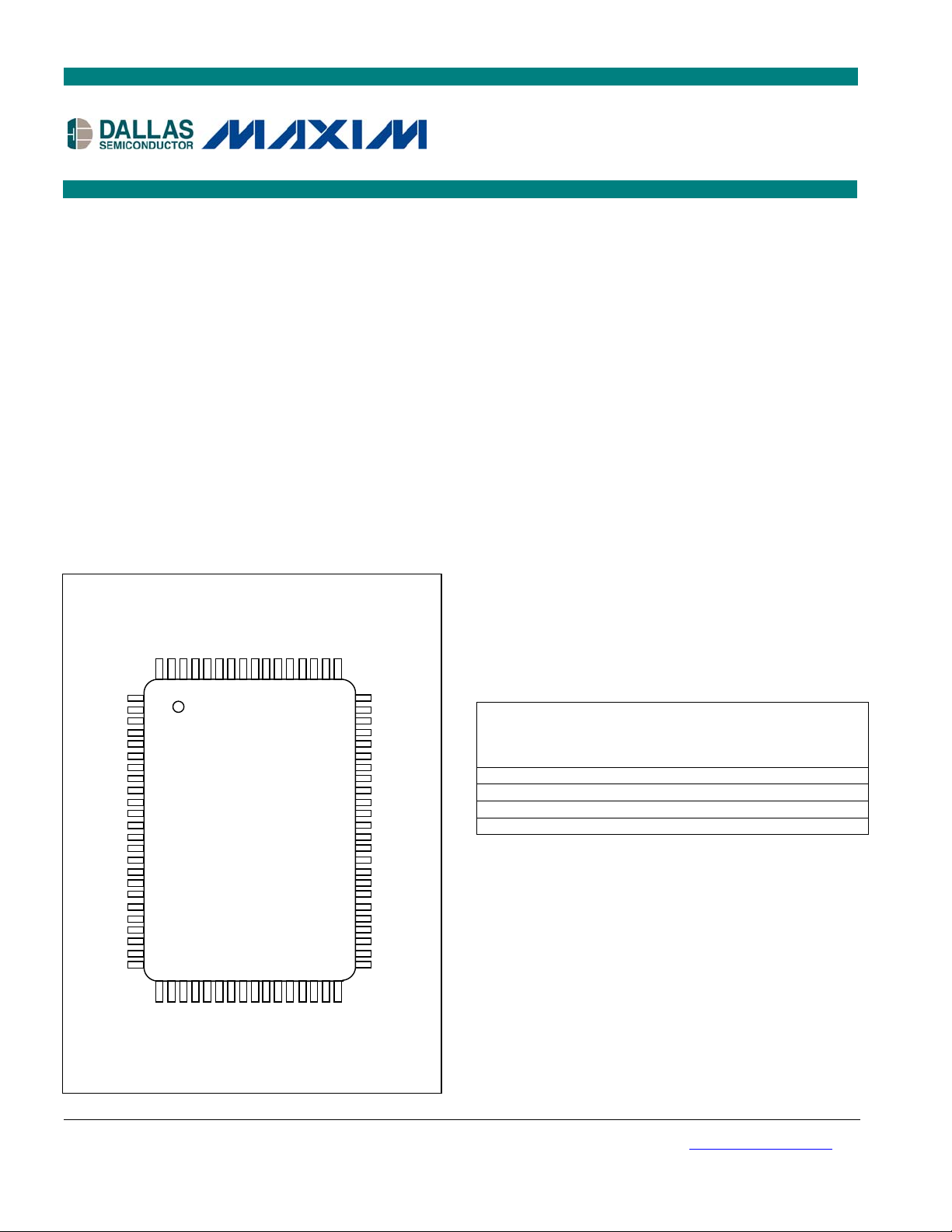
PIN CONFIGURATION
TOP VIEW
E
E1N
BD7
ALE
P0.6/AD6
BA10
P0.7/AD7
N.C.
BD6
Dallas
Semiconductor
DS5002FP
N.C.
BD5
P2.7/A15
P2.6/A14
64
63
62
61
60
59
58
57
56
55
54
53
52
51
50
49
48
47
46
45
44
43
42
41
BD3
P2.5/A13
BD2
P2.4/A12
BD1
P2.3/A11
BD0
VLI
SDI
GND
P2.2/A10
P2.1/A9
P2.0/A8
XTAL1
XTAL2
P3.7/RD
P3.6/WR
P3.5/TI
RST
P3.4/T0
P0.3/AD3
P0.2/AD2
P0.1/AD1
P0.0/AD0
P0.4AD4
BA9
BA8
BA13
R/
V
V
MSEL
P1.0
BA14
P1.1
BA12
P1.2
BA7
P1.3
BA6
E
BA11
P0.5/AD5
80 79 78 77 76 75 74 73 72 71 70 69 68 67 66 65
1
2
3
4
5
6
7
8
9
10
11
12
CC0
13
CC
14
15
16
17
18
19
20
21
22
23
24
25 26 27 28 29 30 31 32 33 34 35 36 37 38 39 40
FEATURES
8051-Compatible Microprocessor for
Secure/Sensitive Applications
Access 32kB, 64kB, or 128kB of NV SRAM for
Program and/or Data Storage
In-System Programming Through On-Chip Serial
Port
Can Modify Its Own Program or Data Memory in
the End System
Firmware Security Features
Memory Stored in Encrypted Form
Encryption Using On-Chip 64-Bit Key
Automatic True Random Key Generator
Self Destruct Input (SDI)
Optional Top Coating Prevents Microprobe
(DS5002FPM)
Improved Security Over Previous Generations
Protects Memory Contents from Piracy
Crash-Proof Operation
Maintains All Nonvolatile Resources for Over 10
Years in the Absence of Power
Power-Fail Reset
Early Warning Power-Fail Interrupt
Watchdog Timer
ORDERING INFORMATION
INTERNAL
PART TEMP RANGE
MICRO
PROBE
SHIELD
DS5002FPM-16 0°C to +70°C Yes 80 QFP
DS5002FPM-16+ 0°C to +70°C Yes 80 QFP
DS5002FMN-16 -40°C to +85°C Yes 80 QFP
DS5002FMN-16+ -40°C to +85°C Yes 80 QFP
+ Denotes a Pb-free/RoHS-compliant device.
Selector Guide appears at end of data sheet.
PINPACKAGE
BA5
BA4
BA3
BA2
BA1
BA0
P1.4
P1.5
P1.6
P1.7
PRO
RST
P3.1/TXD
P3.0/RXD
P3.2/INT0
P3.3/INT1
QFP
Note: Some revisions of this device may incorporate deviations from published specifications known as errata. Multiple revisions of any device
may be simultaneously available through various sales channels. For information about device errata, click here: www.maxim-ic.com/errata
1 of 25
REV: 072806
.
Page 2
DS5002FP Secure Microprocessor Chip
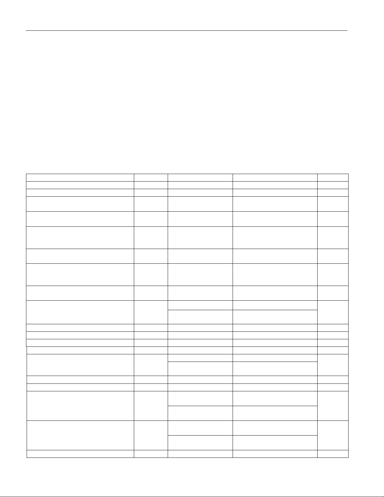
ELECTRICAL SPECIFICATIONS
The DS5002FP adheres to all AC and DC electrical specifications published for the DS5001FP.
ABSOLUTE MAXIMUM RATINGS
Voltage Range on Any Pin Relative to Ground……………………………………………………….-0.3V to (VCC + 0.5V)
Voltage Range on V
Operating Temperature Range………………………………………………………………………………..-40°C to +85°C
Storage Temperature* ...……………………………………………………………………………………..-55°C to +125°C
Soldering Temperature……………………………………………………….....See IPC/JEDEC J-STD-020 Specification
This is a stress rating only and functional operation of the device at these or any other conditions beyond those indicated in the operation
sections of this specification is not implied. Exposure to absolute maximum rating conditions for extended periods of time can affect reliability.
Relative to Ground……………………………………………………………………-0.3V to +6.0V
CC
*Storage temperature is defined as the temperature of the device when V
battery-backed and are undefined.
= 0V and VLI = 0V. In this state the contents of SRAM are not
CC
DC CHARACTERISTICS
(VCC = 5V ±10%, TA = 0°C to +70°C.)**
PARAMETER SYMBOL CONDITIONS MIN TYP MAX UNITS
Input Low Voltage VIL (Note 1) -0.3 +0.8 V
Input High Voltage V
Input High Voltage
(RST, XTAL1,
PROG)
Output Low Voltage at IOL = 1.6mA
(Ports 1, 2, 3,
PF)
Output Low Voltage at IOL = 3.2mA
(Ports 0, ALE, BA15–0, BD7–0,
R/
W, CE1N, CE 1–4, PE 1–4, V
RST
)
Output High Voltage at IOH = -80µA
(Ports 1, 2, 3)
Output High Voltage at IOH = -400µA
(Ports 0, ALE, BA15–0, BD7–0,
W, CE1N, CE 1–4, PE 1–4, V
R/
RST
)
Input Low Current
V
= 0.45V (Ports 1, 2, 3)
IN
Transition Current; 1 to 0
V
= 2.0V (Ports 1, 2, 3)
IN
SDI Input Low Voltage V
SDI Input High Voltage V
SDI Pulldown Resistor R
Input Leakage (Port 0, MSEL) IIL 0.45 < VIN < VCC +10 µA
RST Pulldown Resistor RRE
VRST Pullup Resistor
PROG Pullup Resistor
Power-Fail Warning Voltage V
Minimum Operating Voltage V
Operating Voltage VCC (Note 1)
(Note 1) 2.0 VCC + 0.3 V
IH1
V
(Note 1) 3.5 VCC + 0.3 V
IH2
(Notes 1, 13) 0.15 0.45 V
V
OL1
V
(Note 1) 0.15 0.45 V
OL2
V
(Note 1) 2.4 4.8 V
OH1
(Note 1) 2.4 4.8 V
V
OH2
-50 µA
I
IL
0°C to +70°C -500
I
TL
ILS
IHS
SDI
-40°C to +85°C
(Note 12)
-600
(Note 1) 0.4 V
(Notes 1, 11) 2.0 V
V
CCO
25 60 kΩ
µA
0°C to +70°C 40 150
-40°C to +85°C
(Note 12)
4.7 kΩ
R
VR
40 kΩ
R
PR
0°C to +70°C
PFW
-40°C to +85°C
(Note 1)
(Notes 1, 12)
0°C to +70°C
CCMIN
-40°C to +85°C
(Note 1)
(Notes 1, 12)
30 180
4.25 4.37 4.5
4.1 4.37 4.6
4.00 4.12 4.25
3.85 4.09 4.25
V
CCMIN
5.5 V
kΩ
V
V
2 of 25
Page 3
DS5002FP Secure Microprocessor Chip
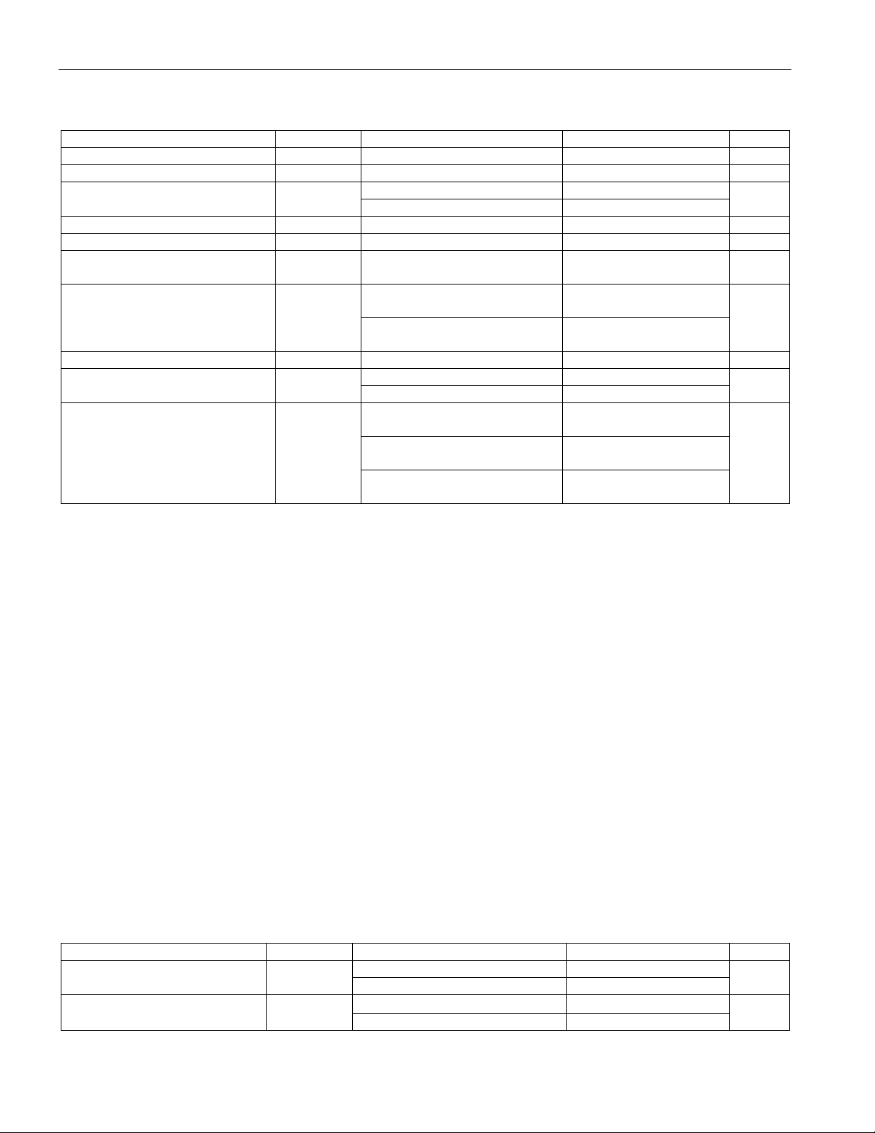
DC CHARACTERISTICS (continued)
(VCC = 5V ±10%, TA = 0°C to +70°C.)**
PARAMETER SYMBOL CONDITIONS MIN TYP MAX UNITS
Lithium Supply Voltage VLI (Note 1) 2.5 4.0 V
Operating Current at 16MHz ICC (Note 2) 36 mA
Idle Mode Current at 12MHz I
Stop Mode Current I
IDLE
STOP
0°C to +70°C (Note 3) 7.0
-40°C to +85°C (Notes 3, 12) 8.0
mA
(Note 4) 80 µA
Pin Capacitance CIN (Note 5) 10 pF
V
Output Supply Voltage (V
Output Supply Battery-Backed
Mode (V
, CE1–4, PE 1–2)
CCO
Output Supply Current (Note 6) I
) V
CCO
V
CCO1
CCO1
CCO2
Current (Note 7)
Reset Trip Point in Stop Mode
(Notes 1, 2)
0°C to +70°C (Notes 1, 8)
-40°C to +85°C (Notes 1, 8,
12)
V
I
LI
CCO
0°C to +70°C 5 75 Lithium-Backed Quiescent
-40°C to +85°C 75 500
BAT = 3.0V (0°C to +70°C)
(Note 1)
BAT = 3.0V (-40°C to +85°C)
(Notes 1, 12)
BAT = 3.3V (0°C to +70°C)
(Note 1)
= VCC - 0.45V 75 mA
CC
-0.45
V
LI
-0.65
V
LI
-0.9
V
4.0 4.25
3.85 4.25
4.4 4.65
V
nA
**All parameters apply to both commercial and industrial temperature operation unless otherwise noted.
Note 1: All voltages are referenced to ground.
Note 2: Maximum operating ICC is measured with all output pins disconnected; XTAL1 driven with t
Note 3: Idle mode I
Note4: Stop mode I
Note 5: Pin capacitance is measured with a test frequency: 1MHz, TA = +25°C.
Note 6: I
Note 7:
Note 8: V
Note 9: Crystal startup time is the time required to get the mass of the crystal into vibrational motion from the time that power is first
Note 10: SDI is deglitched to prevent accidental destruction. The pulse must be longer than t
Note 11: V
Note 12: This parameter applies to industrial temperature operation.
Note 13:
disconnected; RST = PORT0 = V
is measured with all output pins disconnected; XTAL1 driven with t
disconnected; PORT0 = V
V
SS
CCO1
is the current drawn from VLI input when VCC = 0V and V
I
LI
V
BAT
CCO2
applied to the circuit until the first clock pulse is produced by the on-chip oscillator. The user should check with the crystal
vendor for a worst-case specification on this time.
guaranteed unless it is longer than t
IHS
PF pin operation is specified with V
IDLE
is measured with all output pins disconnected; PORT0 = VCC; XTAL2 not connected; RST = MSEL = XTAL1 =
.
STOP
is the maximum average operating current that can be drawn from V
; V
should be ≤ V
SDI
is measured with VCC < VLI, and a maximum load of 10µA on V
minimum is 2.0V or V
, RST = MSEL = VSS.
CC
for I
ILS
, whichever is lower.
CCO
, MSEL = VSS.
CC
max.
BAT
SPA
BAT
.
≥ 3.0V.
, t
CLKR
= 10ns, VIL = 0.5V; XTAL2
CLKR,tCLKF
in normal operation.
CCO
is disconnected. Battery-backed mode is 2.5V ≤ V
CCO
.
CCO
= 10 ns, VIL = 0.5V; XTAL2
CLKF
≤ 4.0; VCC ≤
BAT
to pass the deglitcher, but SDI is not
SPR
AC CHARACTERISTICS—SDI PIN
(VCC = 0V to 5V, TA = 0°C to +70°C.)
PARAMETER SYMBOL CONDITIONS MIN TYP MAX UNITS
SDI Pulse Reject (Note 10) t
SDI Pulse Accept (Note 10) t
SPR
SPA
4.5V < VCC < 5.5V 1.3
V
CC
= 0V, V
= 2.9V 4
BAT
4.5V < VCC < 5.5V 10
V
= 0V, V
CC
= 2.9V 50
BAT
µs
µs
3 of 3
Page 4
DS5002FP Secure Microprocessor Chip
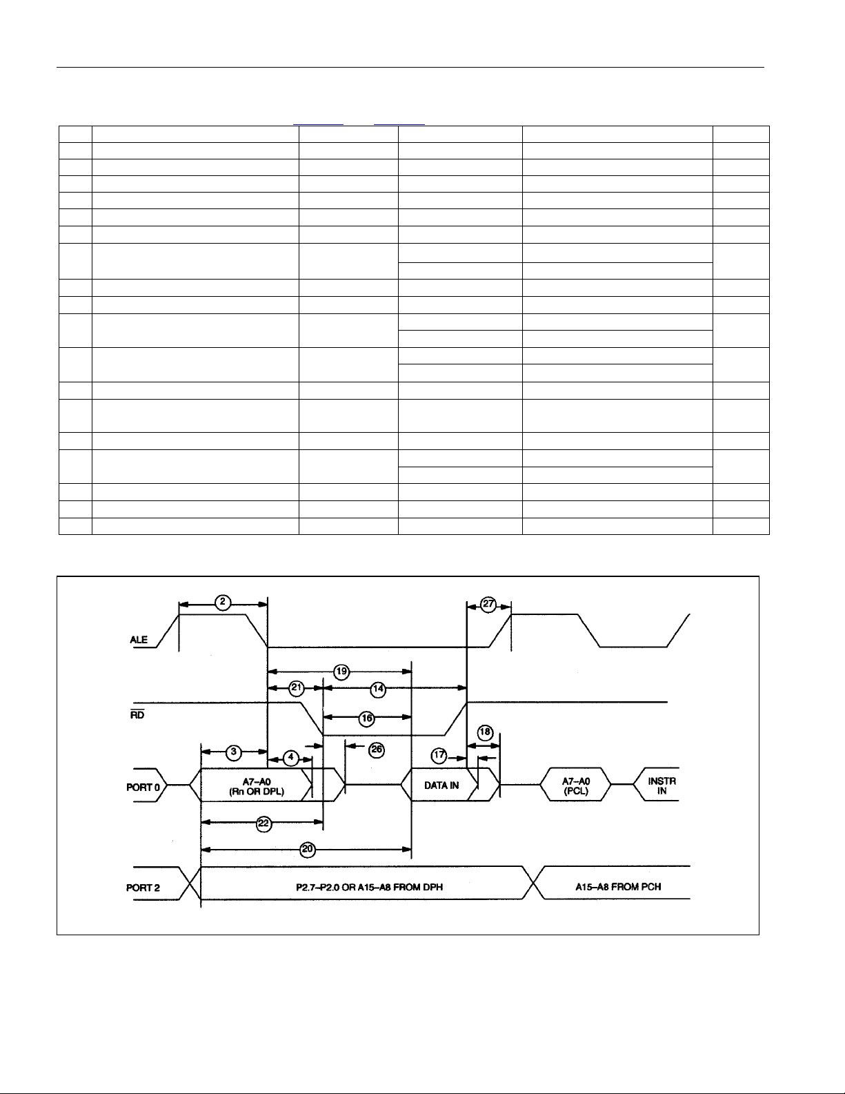
AC CHARACTERISTICS—EXPANDED BUS MODE TIMING SPECIFICATIONS
(VCC = 5V ±10%, TA = 0°C to +70°C.) (Figure 1 and Figure 2)
# PARAMETER SYMBOL CONDITIONS MIN MAX UNITS
1 Oscillator Frequency 1 / t
2 ALE Pulse Width t
3 Address Valid to ALE Low t
4 Address Hold After ALE Low t
14
RD Pulse Width
15
WR Pulse Width
16
RD Low to Valid Data In
17
Data Hold after
18
Data Float after
RD High
RD High
19 ALE Low to Valid Data In t
20 Valid Address to Valid Data In t
21
ALE Low to
Address Valid to
22
Low
23
Data Valid to
24
Data Valid to
25
Data Valid after
26
RD Low to Address Float
27
RD or WR High to ALE High
RD or WR Low
RD or WR
WR Going Low
WR High
WR High
Figure 1. Expanded Data Memory Read Cycle
1.0 16 MHz
CLK
2t
ALPW
t
AVALL
t
AVAAV
6t
t
RDPW
6t
t
WRPW
t
RDLDV
t
RDHDV
t
RDHDZ
ALLVD
AVDV
t
ALLRDL
t
AVRDL
t
DVWRL
t
DVWRH
t
WRHDV
t
RDLAZ
t
RDHALH
12MHz 5t
16MHz 5t
0 ns
2t
12MHz 8t
16MHz 8t
12MHz 9t
16MHz 9t
3t
4t
t
12MHz 7t
16MHz 7t
t
0 ns
t
- 40 ns
CLK
- 40 ns
CLK
- 35 ns
CLK
- 100 ns
CLK
- 100 ns
CLK
- 165
CLK
- 105
CLK
- 70 ns
CLK
- 150
CLK
- 90
CLK
- 165
CLK
- 105
CLK
- 50 3t
CLK
- 130 ns
CLK
- 60 ns
CLK
- 150
CLK
- 90
CLK
-50 ns
CLK
- 40 t
CLK
+ 50 ns
CLK
+ 50 ns
CLK
ns
ns
ns
ns
4 of 25
Page 5
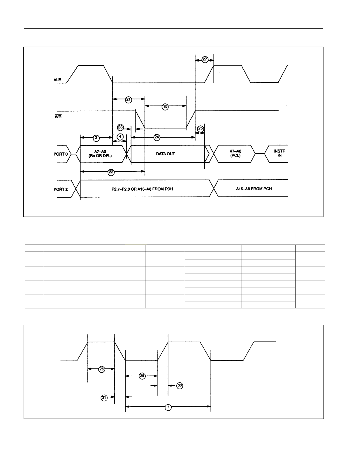
Figure 2. Expanded Data Memory Write Cycle
DS5002FP Secure Microprocessor Chip
AC CHARACTERISTICS—EXTERNAL CLOCK DRIVE
(VCC = 5V ± 10%, TA = 0°C to +70°C.) (Figure 3)
# PARAMETER SYMBOL CONDITIONS MIN MAX UNITS
28 External Clock High Time t
29 External Clock Low Time t
30 External Clock Rise Time t
31 External Clock Fall Time t
Figure 3. External Clock Timing
CLKHPW
CLKLPW
CLKR
CLKF
12MHz 20
16MHz 15
12MHz 20
16MHz 15
12MHz 20
16MHz 15
12MHz 20
16MHz 15
ns
ns
ns
ns
5 of 25
Page 6
DS5002FP Secure Microprocessor Chip
AC CHARACTERISTICS—POWER CYCLE TIME
(VCC = 5V ±10%, TA = 0°C to +70°C.) (Figure 4)
# PARAMETER SYMBOL MIN MAX UNITS
32 Slew Rate from V
33 Crystal Startup Time t
34 Power-on Reset Delay t
Figure 4. Power Cycle Timing
to VLI t
CCMIN
130 µs
F
(Note 9)
CSU
21504 t
POR
CLK
6 of 25
Page 7
DS5002FP Secure Microprocessor Chip
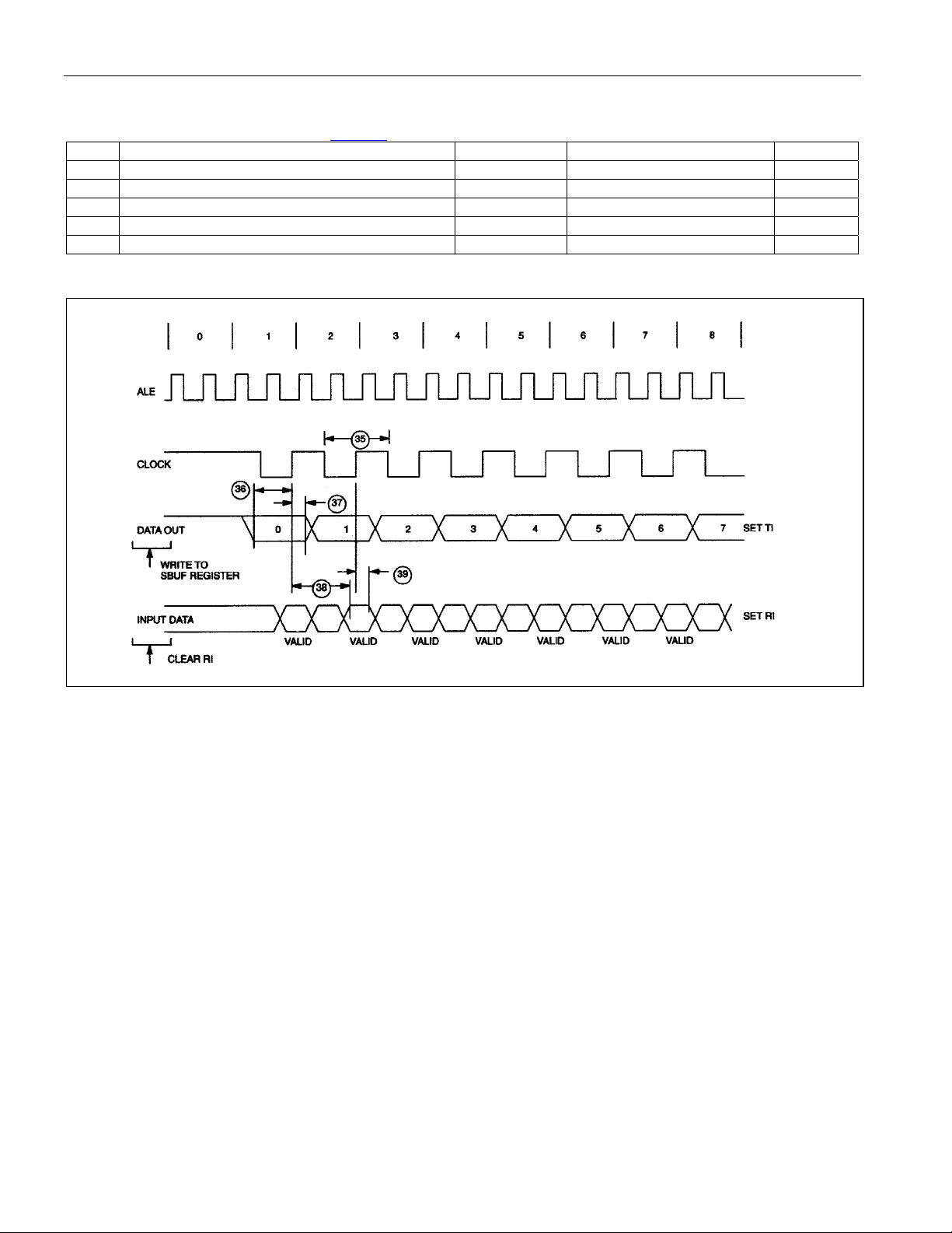
AC CHARACTERISTICS—SERIAL PORT TIMING, MODE 0
(VCC = 5V ±10%, TA = 0°C to +70°C.) (Figure 5)
# PARAMETER SYMBOL MIN MAX UNITS
35 Serial Port Clock Cycle Time t
36 Output Data Setup to Rising Clock Edge t
37 Output Data Hold after Rising Clock Edge t
38 Clock Rising Edge to Input Data Valid t
39 Input Data Hold after Rising Clock Edge t
Figure 5. Serial Port Timing, Mode 0
12t
SPCLK
10t
DOCH
2t
CHDO
10t
CHDV
0 ns
CHDIV
µs
CLK
- 133 ns
CLK
- 117 ns
CLK
- 133 ns
CLK
7 of 25
Page 8
DS5002FP Secure Microprocessor Chip
AC CHARACTERISTICS—BYTE-WIDE ADDRESS/DATA BUS TIMING
(VCC = 5V ±10%, TA = 0°C to +70°C.) (Figure 6)
# PARAMETER SYMBOL MIN MAX UNITS
Delay to Byte-Wide Address Valid from
40
CE2, or CE1N Low During Op Code Fetch
41
Pulse Width of
Byte-Wide Address Hold After
42
CE1N High During Op Code Fetch
Byte-Wide Data Setup to
43
High During Op Code Fetch
CE1–4, PE1–4, or CE1N
CE1, CE2, or CE1N
CE1, CE2, or
CE1,
30 ns
t
CE1LPA
t
CEPW
t
CE1HPA
t
OVCE1H
4t
2t
1t
- 35 ns
CLK
- 20 ns
CLK
+ 40 ns
CLK
Byte-Wide Data Hold After
44
High During Op Code Fetch
Byte-Wide Address Hold After
45
CE1N High During MOVX
Delay from Byte-Wide Address Valid
46
PE1–4, or CE1N Low During MOVX
Byte-Wide Data Setup to
47
CE1N High During MOVX (Read)
Byte-Wide Data Hold After
48
CE1N High During MOVX (Read)
Byte-Wide Address Valid to R/
49
MOVX (Write)
Delay from R/
50
MOVX (Write)
Valid Data Out Hold Time from
51
CE1N High
52
Valid Data Out Hold Time from R/
53
Write Pulse Width (R/
W Low to Valid Data Out During
CE1, CE2, or CE1N
CE1–4, PE1–4, or
CE1–4, PE1–4, or
W Active During
W Low Time)
Figure 6. Byte-Wide Bus Timing
CE1–4, PE1–4, or
CE1–4,
CE1–4, PE1–4, or
W High
0 ns
t
CE1HOV
4t
t
CEHDA
4t
t
CELDA
1t
t
DACEH
0 ns
t
CEHDV
t
3t
AVRWL
20 ns
t
RWLDV
1t
t
CEHDV
0 ns
t
RWHDV
t
6t
RWLPW
- 30 ns
CLK
- 35 ns
CLK
+ 40 ns
CLK
- 35 ns
CLK
- 15 ns
CLK
- 20 ns
CLK
8 of 25
Page 9

DS5002FP Secure Microprocessor Chip
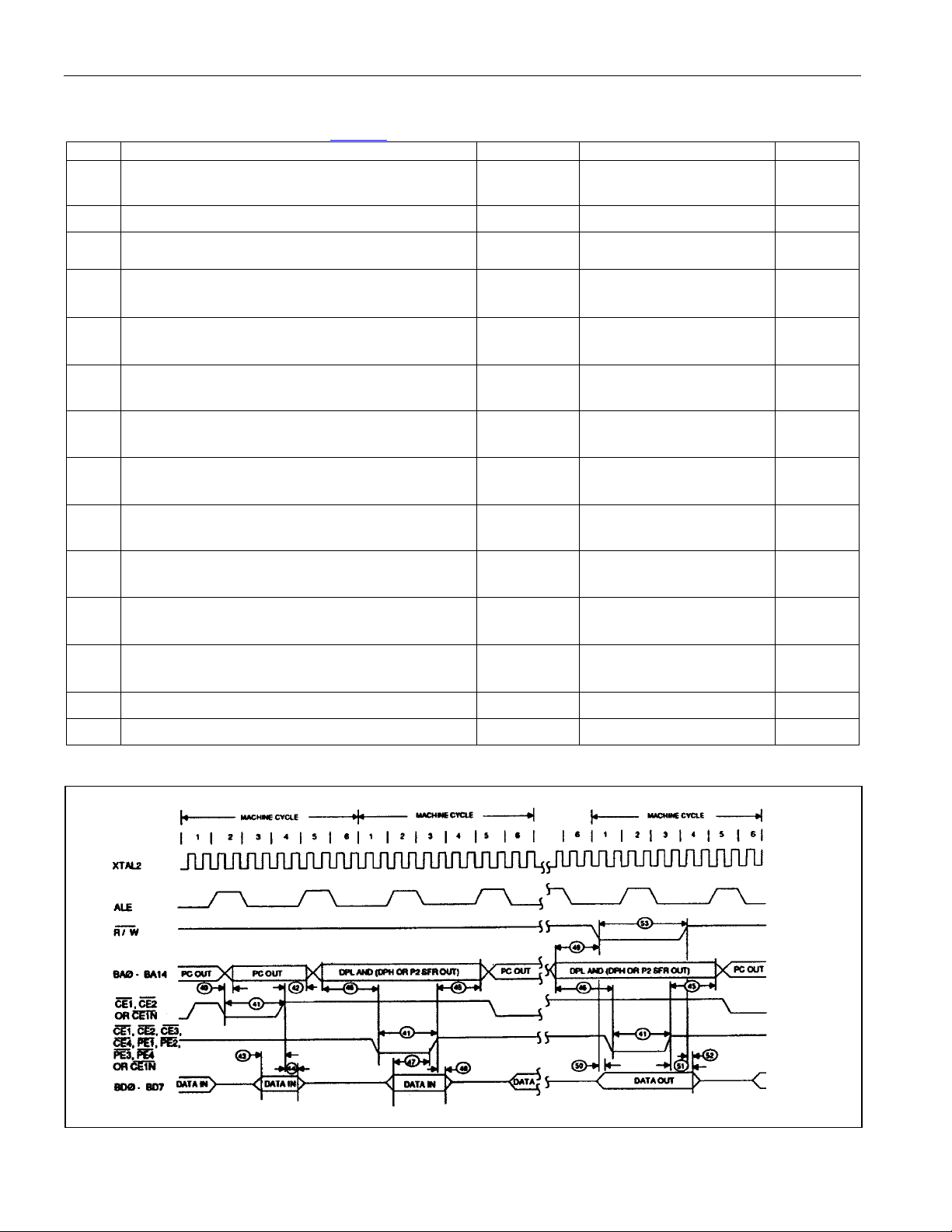
RPC AC CHARACTERISTICS, DBB READ
(VCC = 5V ±10%, TA = 0°C to +70°C.) (Figure 7)
# PARAMETER SYMBOL MIN MAX UNITS
54
CS, A
Setup to RD
0
55
CS, A
Hold After RD
0
56
RD Pulse Width
57
CS, A
to Data Out Delay
0
58
RD to Data Out Delay
59
RD to Data Float Delay
0 ns
t
AR
0 ns
t
RA
160 ns
t
RR
t
130 ns
AD
0 130 ns
t
RD
85 ns
t
RDZ
RPC AC CHARACTERISTICS, DBB WRITE
(VCC = 5V ±10%, TA = 0°C to +70°C.) (Figure 7)
# PARAMETER SYMBOL MIN MAX UNITS
60
61A
61B
62
63
64
CS, A
Setup to WR
0
CS, Hold After WR
A
, Hold After WR
0
WR Pulse Width
Data Setup to
Data Hold After
WR
WR
t
0 ns
AW
0 ns
t
WA
20 ns
t
WA
160 ns
t
WW
130 ns
t
DW
20 ns
t
WD
AC CHARACTERISTICS, DMA
(VCC = 5V ±10%, TA = 0°C to +70°C.)
# PARAMETER SYMBOL MIN MAX UNITS
65
DACK to WR or RD
t
0 ns
ACC
66
RD or WR to DACK
67
DACK to Data Valid
68
RD or WR to DRQ Cleared
0 ns
t
CAC
0 130 ns
t
ACD
110 ns
t
CRQ
AC CHARACTERISTICS, PROG
(VCC = 5V ±10%, TA = 0°C to +70°C.)
# PARAMETER SYMBOL MIN MAX UNITS
69
PROG Low to Active
70
PROG High to Inactive
9 of 25
t
48 CLKS
PRA
48 CLKS
t
PRI
Page 10

Figure 7. RPC Timing Mode
DS5002FP Secure Microprocessor Chip
10 of 25
Page 11

DS5002FP Secure Microprocessor Chip
PIN DESCRIPTION
PIN NAME FUNCTION
11, 9, 7, 5,
1, 79, 77,
P0.0–P0.7
75
15, 17, 19,
21, 25, 27,
P1.0–P1.7
29, 31
49, 50, 51,
56, 58, 60,
P2.0–P2.7
64, 66
36 P3.0/RXD
38 P3.1/TXD
39
40
P3.2/INT0
P3.3/INT1
41 P3.4/T0
44 P3.5/T1
45
46
P3.6/WR
P3.7/RD
34 RST
70 ALE
47, 48 XTAL2, XTAL1
52 GND
13 VCC
12 V
CCO
54 VLI
16, 8, 18,
80, 76, 4, 6,
20, 24, 26,
BA14–BA0
28, 30, 33,
35, 37
71, 69, 67,
65, 61, 59,
BD7–BD0
57, 55
10
74
2
63
R/W
CE1
CE2
CE3
General-Purpose I/O Port 0. This port is open-drain and cannot drive a logic 1. It requires
external pullups. Port 0 is also the multiplexed expanded address/data bus. When used in
this mode, it does not require pullups.
General-Purpose I/O Port 1
General-Purpose I/O Port 2. Also serves as the MSB of the expanded address bus.
General-Purpose I/O Port Pin 3.0. Also serves as the receive signal for the on-board UART.
This pin should not be connected directly to a PC COM port.
General-Purpose I/O Port Pin 3.1. Also serves as the transmit signal for the on-board
UART. This pin should not be connected directly to a PC COM port.
General-Purpose I/O Port Pin 3.2. Also serves as the active-low external interrupt 0.
General-Purpose I/O Port Pin 3.3. Also serves as the active-low external interrupt 1.
General-Purpose I/O Port Pin 3.4. Also serves as the timer 0 input.
General-Purpose I/O Port Pin 3.5. Also serves as the timer 1 input.
General-Purpose I/O Port Pin. Also serves as the write strobe for Expanded bus operation.
General-Purpose I/O Port Pin. Also serves as the read strobe for Expanded bus operation.
Active-High Reset Input. A logic 1 applied to this pin activates a reset state. This pin is
pulled down internally so this pin can be left unconnected if not used. An RC power-on reset
circuit is not needed and is not recommended.
Address Latch Enable. Used to demultiplex the multiplexed expanded address/data bus on
port 0. This pin is normally connected to the clock input on a ’373 type transparent latch.
Crystal Connections. Used to connect an external crystal to the internal oscillator. XTAL1 is
the input to an inverting amplifier and XTAL2 is the output.
Logic Ground
Power Supply, +5V
V
Output. This is switched between VCC and VLI by internal circuits based on the level of
CC
. When power is above the lithium input, power is drawn from VCC. The lithium cell
V
CC
remains isolated from a load. When V
should be connected to the VCC pin of an SRAM.
V
CCO
is below VLI, the V
CC
Lithium Voltage Input. Connect to a lithium cell greater than V
as shown in the electrical specifications. Nominal value is +3V.
V
LIMAX
Byte-Wide Address Bus Bits 14–0. This bus is combined with the nonmultiplexed data bus
(BD7–BD0) to access NV SRAM. Decoding is performed using CE1 to CE4. Therefore, BA15
is not actually needed. Read/write access is controlled by R/W. BA14–0 connect directly to an
8k, 32k, or 128k SRAM. If an 8k RAM is used, BA13 and BA14 are unconnected. If a 128k
SRAM is used, the micro converts CE2 and CE3 to serve as A16 and A15, respectively.
Byte-Wide Data Bus Bits 7–0. This 8-bit bidirectional bus is combined with the
nonmultiplexed address bus (BA14–BA0) to access NV SRAM. Decoding is performed on
CE1 and CE2. Read/write access is controlled by R/W. D7–D0 connect directly to an SRAM,
and optionally to a real-time clock or other peripheral.
Read/Write (Active Low). This signal provides the write enable to the SRAMs on the bytewide bus. It is controlled by the memory map and partition. The blocks selected as program
(ROM) are write-protected.
Active-Low Chip Enable 1. This is the primary decoded chip enable for memory access on
the byte-wide bus. It connects to the chip-enable input of one SRAM. CE1 is lithium-backed.
It remains in a logic-high inactive state when VCC falls below VLI.
Active-Low Chip Enable 2. This chip enable is provided to access a second 32k block of
memory. It connects to the chip-enable input of one SRAM. When MSEL = 0, the micro
converts CE2 into A16 for a 128k x 8 SRAM. CE2 is lithium-backed and remains at a logic
high when V
falls below VLI.
CC
Active-Low Chip Enable 3. This chip enable is provided to access a third 32k block of
memory. It connects to the chip enable input of one SRAM. When MSEL = 0, the micro
converts CE3 into A15 for a 128k x 8 SRAM. CE3 is lithium-backed and remains at a logic
high when V
falls below VLI.
CC
11 of 25
switches to the VLI source.
CCO
and no greater than
LIMIN
Page 12

DS5002FP Secure Microprocessor Chip
PIN NAME FUNCTION
Active-Low Chip Enable 4. This chip enable is provided to access a fourth 32k block of
62
78
3
22
23
32
42
43
CE4
PE1
PE2
PE3
PE4
PROG
VRST
PF
14 MSEL
53 SDI
72
CE1N
memory. It connects to the chip-enable input of one SRAM. When MSEL = 0, this signal is
unused. CE4 is lithium-backed and remains at a logic high when V
Active-Low Peripheral Enable 1. Accesses data memory between addresses 0000h and
3FFFh when the PES bit is set to a logic 1. Commonly used to chip enable a byte-wide realtime clock such as the DS1283. PE1 is lithium-backed and will remain at a logic high when
falls below VLI. Connect PE1 to battery-backed functions only.
V
CC
Active-Low Peripheral Enable 2. Accesses data memory between addresses 4000h and
7FFFh when the PES bit is set to a logic 1. PE2 is lithium-backed and will remain at a logic
high when V
falls below VLI. Connect PE2 to battery-backed functions only.
CC
Active-Low Peripheral Enable 3. Accesses data memory between addresses 8000h and
BFFFh when the PES bit is set to a logic 1. PE3 is not lithium-backed and can be connected
to any type of peripheral function. If connected to a battery-backed chip, it will need additional
circuitry to maintain the chip enable in an inactive state when V
Active-Low Peripheral Enable 4. Accesses data memory between addresses C000h and
FFFFh when the PES bit is set to a logic 1. PE4 is not lithium-backed and can be connected
to any type of peripheral function. If connected to a battery-backed chip, it will need additional
circuitry to maintain the chip enable in an inactive state when V
Invokes the Bootstrap Loader on Falling Edge. This signal should be debounced so that
only one edge is detected. If connected to ground, the micro enters bootstrap loading on
power-up. This signal is pulled up internally.
This I/O pin (open drain with internal pullup) indicates that the power supply (VCC) has
fallen below the V
level and the micro is in a reset state. When this occurs, the
CCMIN
DS5002FP drives this pin to a logic 0. Because the micro is lithium-backed, this signal is
guaranteed even when V
= 0V. Because it is an I/O pin, it also forces a reset if pulled low
CC
externally. This allows multiple parts to synchronize their power-down resets.
This output goes to a logic 0 to indicate that the micro has switched to lithium backup.
This corresponds to V
even when V
= 0V. The normal application of this signal is to control lithium-powered
CC
< VLI. Because the micro is lithium-backed, this signal is guaranteed
CC
current to isolate battery-backed functions from non-battery-backed functions.
Memory Select. This signal controls the memory size selection. When MSEL = +5V, the
DS5002FP expects to use 32k x 8 SRAMs. When MSEL = 0V, the DS5002FP expects to use
a 128k x 8 SRAM. MSEL must be connected regardless of partition, mode, etc.
Self-Destruct Input. An active high on this pin causes an unlock procedure. This results in
the destruction of Vector RAM, Encryption Keys, and the loss of power from V
should be grounded if not used.
Non-Battery-Backed Version of CE1. It is not generally useful since the DS5002FP cannot
be used with EPROM due to its encryption.
falls below VLI.
CC
< VLI.
CC
< VLI.
CC
. This pin
CCO
73 N.C.
No Connection
12 of 25
Page 13

DS5002FP Secure Microprocessor Chip
DETAILED DESCRIPTION
The DS5002FP implements a security system that is an improved version of its predecessor, the DS5000FP. Like
the DS5000FP, the DS5002FP loads and executes application software in encrypted form. Up to 128kB of
standard SRAM can be accessed by its byte-wide bus. This RAM is converted by the DS5002FP into lithiumbacked nonvolatile storage for program and data. Data is maintained for over 10 years at room temperature with a
very small lithium cell. As a result, the contents of the RAM and the execution of the software appear unintelligible
to the outside observer. The encryption algorithm uses an internally stored and protected key. Any attempt to
discover the key value results in its erasure, rendering the encrypted contents of the RAM useless.
The secure microprocessor chip offers a number of major enhancements to the software security implemented in
the previous generation DS5000FP. First, the DS5002FP provides a stronger software encryption algorithm that
incorporates elements of DES encryption. Second, the encryption is based on a 64-bit key word, as compared to
the DS5000FP’s 40-bit key. Third, the key can only be loaded from an on-chip true random-number generator. As a
result, the true key value is never known by the user. Fourth, a self-destruct input (SDI) pin is provided to interface
to external tamper-detection circuitry. With or without the presence of V
effect as resetting the security lock: immediate erasure of the key word and the 48-byte Vector RAM area. Fifth, an
optional top-coating of the die prevents access of information using microprobing techniques. Finally, customerspecific versions of the DS5002FP are available that incorporate a one-of-a-kind encryption algorithm.
When implemented as a part of a secure system design, a system based on the DS5002FP can typically provide a
level of security that requires more time and resources to defeat than it is worth to unauthorized individuals who
have reason to try. For a user who wants a preconstructed module using the DS5002FP, RAM, lithium cell, and a
real-time clock, the DS2252T is available and described in a separate data sheet.
, activation of the SDI pin has the same
CC
BLOCK DIAGRAM
Figure 8 is a block diagram illustrating the internal architecture of the DS5002FP. The DS5002FP is a secure
implementation of the DS5001FP 128k soft microprocessor chip. As a result, it operates in an identical fashion to
the DS5001FP, except where indicated. See the DS5001FP data sheet for operating details.
13 of 25
Page 14
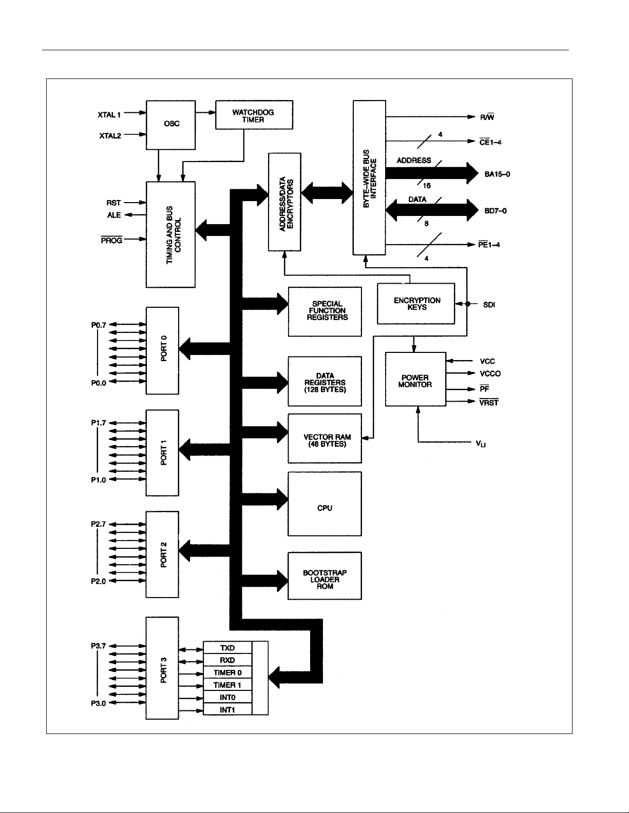
Figure 8. Block Diagram
DS5002FP Secure Microprocessor Chip
14 of 25
Page 15

DS5002FP Secure Microprocessor Chip
SECURE OPERATION OVERVIEW
The DS5002FP incorporates encryption of the activity on its byte-wide address/data bus to prevent unauthorized
access to the program and data information contained in the NV RAM. Loading an application program in this
manner is performed by the bootstrap loader using the general sequence described below:
1) Clear security lock.
2) Set memory map configuration as for DS5001FP
3) Load application software
4) Set security lock
5) Exit loader
Loading of application software into the program/data RAM is performed while the DS5002FP is in its bootstrap
load mode. Loading is only possible when the security lock is clear. If the security lock has previously set, then it
must be cleared by issuing the “Z” command from the bootstrap loader. Resetting the security lock instantly clears
the previous key word and the contents of the Vector RAM. In addition, the bootstrap ROM writes 0’s into the first
32k of external RAM.
The user’s application software is loaded into external CMOS SRAM by the “L” command in “scrambled” form
through on-chip encryptor circuits. Each external RAM address is an encrypted representation of an on-chip logical
address. Thus, the sequential instructions of an ordinary program or data table are stored nonsequentially in RAM
memory. The contents of the program/data RAM are also encrypted. Each byte in RAM is encrypted by a key- and
address-dependent encryptor circuit such that identical bytes are stored as different values in different memory
locations.
The encryption of the program/data RAM is dependent on an on-chip 64-bit key word. The key is loaded by the
ROM firmware just prior to the time that the application software is loaded, and is retained as nonvolatile
information in the absence of V
setting the on-chip security lock, which is also retained as nonvolatile information in the absence of V
attempt to tamper with the key word and thereby gain access to the true program/data RAM contents results in the
erasure of the key word as well as the RAM contents.
During execution of the application software, logical addresses on the DS5002FP that are generated from the
program counter or data pointer registers are encrypted before they are presented on the byte-wide address bus.
Op codes and data are read back and decrypted before they are operated on by the CPU. Similarly, data values
written to the external nonvolatile RAM storage during program execution are encrypted before they are presented
on the byte-wide data bus during the write operation. This encryption/decryption process is performed in real time
such that no execution time is lost as compared to the non-encrypted DS5001FP or 8051 running at the same
clock rate. As a result, operation of the encryptor circuitry is transparent to the application software.
Unlike the DS5000FP, the DS5002FP chip’s security feature is always enabled.
by the lithium backup circuits. After loading is complete, the key is protected by
CC
. Any
CC
SECURITY CIRCUITRY
The on-chip functions associated with the DS5002FP’s software security feature are depicted in Figure 9.
Encryption logic consists of an address encryptor and a data encryptor. Although each encryptor uses its own
algorithm for encrypting data, both depend on the 64-bit key word which is contained in the Encryption Key
registers. Both the encryptors operate during loading of the application software and also during its execution.
15 of 25
Page 16

Figure 9. Security Circuitry
DS5002FP Secure Microprocessor Chip
The address encryptor translates each “logical” address, i.e., the normal sequence of addresses that are generated
in the logical flow of program execution, into an encrypted address (or “physical” address) at which the byte is
actually stored. Each time a logical address is generated, either during program loading or during program
execution, the address encryptor circuitry uses the value of the 64-bit key word and of the address itself to form the
physical address, which are presented on the address lines of the RAM. The encryption algorithm is such that there
is one and only one physical address for every possible logical address. The address encryptor operates over the
entire memory range, which is configured during bootstrap loading for access on the byte-wide bus.
As bootstrap loading of the application software is performed, the data encryptor logic transforms the op code,
operand, or data byte at any given memory location into an encrypted representation. As each byte is read back to
the CPU during program execution, the internal data encryptor restores it to its original value. When a byte is
written to the external nonvolatile program/ data RAM during program execution, that byte is stored in encrypted
form as well. The data encryption logic uses the value of the 64-bit key, the logical address to which the data is
being written, and the value of the data itself to form the encrypted data, which is written to the nonvolatile
program/data RAM. The encryption algorithm is repeatable, such that for a given data value, encryption key value,
and logical address the encrypted byte will always be the same. However, there are many possible encrypted data
values for each possible true data value due to the algorithm’s dependency on the values of the logical address
and encryption key.
When the application software is executed, the internal CPU of the DS5002FP operates as normal. Logical
addresses are calculated for op code fetch cycles and also data read and write operations. The DS5002FP has the
ability to perform address encryption on logical addresses as they are generated internally during the normal
course of program execution. In a similar fashion, data is manipulated by the CPU in its true representation.
However, it is also encrypted when it is written to the external program/data RAM, and is restored to its original
value when it is read back.
When an application program is stored in the format described above, it is virtually impossible to disassemble op
codes or to convert data back into its true representation. Address encryption has the effect that the op codes and
data are not stored in the contiguous form in which they were assembled, but rather in seemingly random locations
in memory. This in itself makes
it virtually impossible to determine the normal flow of the program. As an added
16 of 25
Page 17

DS5002FP Secure Microprocessor Chip
protection measure, the address encryptor also generates “dummy” read access cycles whenever time is available
during program execution.
DUMMY READ CYCLES
Like the DS5000FP, the DS5002FP generates a “dummy” read access cycle to non-sequential addresses in
external RAM memory whenever time is available during program execution. This action has the affect of further
complicating the task of determining the normal flow of program execution. During these pseudorandom dummy
cycles, the RAM is read to all appearances, but the data is not used internally. Through the use of a repeatable
exchange of dummy and true read cycles, it is impossible to distinguish a dummy cycle from a real one.
ENCRYPTION ALGORITHM
The DS5002FP incorporates a proprietary algorithm implemented in hardware, which performs the scrambling of
address and data on the byte-wide bus to the SRAM. This algorithm has been greatly strengthened with respect to
its DS5000FP predecessor. Improvements include:
1) 64-bit encryption key
2) Incorporation of DES-like operations to provide a greater degree of nonlinearity
3) Customizable encryption
The encryption circuitry uses a 64-bit key value (compared to the DS5000FP’s 40-bit key), which is stored on the
DS5002FP die and protected by the Security Lock function described below. In addition, the algorithm has been
strengthened to incorporate certain operations used in DES encryption, so that the encryption of both the
addresses and data is highly nonlinear. Unlike the DS5000FP, the encryption circuitry in the DS5002FP is always
enabled.
Dallas Semiconductor can customize the encryption circuitry by laser programming the die to insure that a unique
encryption algorithm is delivered to the customer. In addition, the customer-specific version can be branded as
specified by the customer. Please contact Dallas Semiconductor for ordering information of customer-specific
versions.
ENCRYPTION KEY
As described above, the on-chip 64-bit encryption key is the basis of both the address and data encryptor circuits.
The DS5002FP provides a key management system, which is greatly improved over the DS5000FP. The
DS5002FP does not give the user the ability to select a key. Instead, when the loader is given certain commands,
the key is set based on the value read from an on-chip hardware random number generator. This action is
performed just prior to actually loading the code into the external RAM. This scheme prevents characterization of
the encryption algorithm by continuously loading new, known keys. It also frees the user from the burden of
protecting the key selection process.
The random number generator circuit uses the asynchronous frequency differences of two internal ring oscillator
and the processor master clock (determined by XTAL1 and XTAL2). As a result, a true random number is
produced.
VECTOR RAM
A 48-byte vector RAM area is incorporated on-chip, and is used to contain the reset and interrupt vector code in the
DS5002FP. It is included in the architecture to help insure the security of the application program.
If reset and interrupt vector locations were accessed from the external nonvolatile program/data RAM during the
execution of the program, then it would be possible to determine the encrypted value of known addresses. This
could be done by forcing an interrupt or reset condition and observing the resulting addresses on the byte-wide
address/data bus. For example, it is known that when a hardware reset is applied the logical program address is
forced to location 0000H and code is executed starting from this location. It would then be possible to determine
the encrypted value (or physical address) of the logical address value 0000H by observing the address presented
to the external RAM following a hardware reset. Interrupt vector address relationships could be determined in a
similar fashion. By using the on-chip vector RAM to contain the interrupt and reset vectors, it is impossible to
17 of 25
Page 18

DS5002FP Secure Microprocessor Chip
observe such relationships. Although it is very unlikely that an application program could be deciphered by
observing vector address relationships, the vector RAM eliminates this possibility. Note that the dummy accesses
mentioned above are conducted while fetching from vector RAM.
The vector RAM is automatically loaded with the user’s reset and interrupt vectors during bootstrap loading.
SECURITY LOCK
Once the application program has been loaded into the DS5002FP’s NV RAM, the security lock can be enabled by
issuing the “Z” command in the bootstrap loader. While the security lock is set, no further access to program/data
information is possible by the on-chip ROM. Access is prevented by both the bootstrap loader firmware and the
DS5002FP encryptor circuits.
Access to the NV RAM can only be regained by clearing the security lock by the “U” command in the bootstrap
loader. This action triggers several events, which defeat tampering. First, the encryption key is instantaneously
erased. Without the encryption key, the DS5002FP is no longer able to decrypt the contents of the RAM. Therefore,
the application software can no longer be correctly executed, nor can it be read back in its true form by the
bootstrap loader. Second, the vector RAM area is also instantaneously erased, so that the reset and vector
information is lost. Third, the bootstrap loader firmware sequentially erases the encrypted RAM area. Lastly, the
loader creates and loads a new random key.
The Security Lock bit itself is constructed using a multiple-bit latch which is interlaced for self-destruct in the event
of tampering. The lock is designed to set-up a “domino-effect” such that erasure of the bit will result in an
unstoppable sequence of events that clears critical data including Encryption Key and Vector RAM. In addition, this
bit is protected from probing by the top-coating feature mentioned below.
SELF-DESTRUCT INPUT
The self-destruct input (SDI) pin is an active-high input that is used to reset the security lock in response to an
external event. The SDI input is intended to be used with external tamper-detection circuitry. It can be activated
with or without operating power applied to the V
and causes the same sequence of events described above for this action. In addition, power is momentarily
removed from the byte-wide bus interface including the V
pin. Activation of the SDI pin instantly resets the security lock
CC
pin, resulting in the loss of data in external RAM.
CCO
TOP LAYER COATING
The DS5002FPM is provided with a special top-layer coating that is designed to prevent a probe attack. This
coating is implemented with second-layer metal added through special processing of the microcontroller die. This
additional layer is not a simple sheet of metal, but rather a complex layout that is interwoven with power and
ground, which are in turn connected to logic for the encryption key and the security lock. As a result, any attempt to
remove the layer or probe through it results in the erasure of the security lock and/or the loss of encryption key bits.
BOOTSTRAP LOADING
Initial loading of application software into the DS5002FP is performed by firmware within the on-chip bootstrap
loader communicating with a PC by the on-chip serial port in a manner that is almost identical to that for the
DS5001FP. The user should consult the DS5001FP data sheet as a basis of operational characteristics of this
firmware. Certain differences in loading procedure exist in order to support the security feature. These differences
are documented below. Table 1
When the bootstrap loader is invoked, portions of the 128-byte scratchpad RAM area are automatically overwritten
with 0’s, and then used for variable storage for the bootstrap firmware. Also, a set of 8 bytes are generated using
the random number generator circuitry and are saved as a potential word for the 64-bit encryption key.
Any read or write operation to the DS5002FP’s external program/data SRAM can only take place if the security lock
bit is in a cleared state. Therefore, the first step in loading a program should be the clearing of the security lock bit
through the “U” command.
summarizes the commands accepted by the bootstrap loader.
18 of 25
Page 19

DS5002FP Secure Microprocessor Chip
Table 1. Serial Bootstrap Loader Commands
COMMAND FUNCTION
C Return CRC-16 of the program/data NV RAM
D Dump Intel Hex file
F Fill program/data NV RAM
G Get data from P1, P2, and P3
I N/A on the DS5002FP
L Load Intel Hex file
M Toggle modem available bit
N Set freshness seal—all program and data is lost
P Put data into P0, P1, P2, and P3
R Read status of NV SFRs (MCON, RPCTL, MSL, CALIB)
T Trace (echo) incoming Intel Hex code
U Clear Security Lock
V Verify program/data NV RAM with incoming Intel Hex data
W Write special function registers (MCON, RPCTL, MSL, CALIB)
Z Set security lock
Execution of certain bootstrap loader commands result in the loading of the newly generated 64-bit random number
into the encryption key word. These commands are as follows:
Fill F
Load L
Dump D
Verify V
CRC C
Execution of the Fill and Load commands result in the data loaded into the NV RAM in an encrypted form
determined by the value of the newly generated key word. The subsequent execution of the Dump command within
the same bootstrap session causes the contents of the encrypted RAM to be read out and transmitted back to the
host PC in decrypted form. Similarly, execution of the Verify command within the same bootstrap session causes
the incoming absolute hex data to be compared against the true contents of the encrypted RAM, and the CRC
command returns the CRC value calculated from the true contents of the encrypted RAM. As long as any of the
above commands are executed within the same bootstrap session, the loaded key value remains the same, and
the contents of the encrypted program/data NV RAM can be read or written normally and freely until the security
lock bit is set.
When the security lock bit is set using the Z command, no further access to the true RAM contents is possible
using any bootstrap command or by any other means.
INSTRUCTION SET
The DS5002FP executes an instruction set that is object code-compatible with the industry standard 8051
microcontroller. As a result, software development packages such as assemblers and compilers that have been
written for the 8051 are compatible with the DS5002FP. A complete description of the instruction set and operation
are provided in the Secure Microcontroller User’s Guide.
Also note that the DS5002FP is embodied in the DS2252T module. The DS2252T combines the DS5002FP with
between 32k and 128k of SRAM, a lithium cell, and a real-time clock. This is packaged in a 40-pin SIMM module.
MEMORY ORGANIZATION
Figure 10 illustrates the memory map accessed by the DS5002FP. The entire 64k of program and 64k of data are
potentially available to the byte-wide bus. This preserves the I/O ports for application use. The user controls the
portion of memory that is actually mapped to the byte-wide bus by selecting the program range and data range.
Any area not mapped into the NV RAM is reached by the expanded bus on ports 0 and 2. An alternate
configuration allows dynamic partitioning of a 64k space as shown in Figure 11
another 64k of potential data storage or memory mapped peripheral space as shown in Figure 12
. Selecting PES = 1 provides
. These
19 of 25
Page 20

DS5002FP Secure Microprocessor Chip
selections are made using special function registers. The memory map and its controls are covered in detail in the
Secure Microcontroller User’s Guide.
Figure 10. Memory Map in Nonpartitionable Mode (PM = 1)
20 of 25
Page 21

Figure 11. Memory Map In Partitionable Mode (PM = 0)
DS5002FP Secure Microprocessor Chip
Figure 12. Memory Map with PES = 1
21 of 25
Page 22

DS5002FP Secure Microprocessor Chip
Figure 13
both program and data are stored in a common RAM chip. Figure 14
SRAMs. The byte-wide address bus connects to the SRAM address lines. The bidirectional byte-wide data bus
connects the data I/O lines of the SRAM.
illustrates a typical memory connection for a system using a 128kB SRAM. Note that in this configuration,
shows a similar system with using two 32kB
Figure 13. Connection to 128k x 8 SRAM
22 of 25
Page 23

Figure 14. Connection to 64k x 8 SRAM
DS5002FP Secure Microprocessor Chip
POWER MANAGEMENT
The DS5002FP monitors VCC to provide power-fail reset, early warning power-fail interrupt, and switchover to
lithium backup. It uses an internal bandgap reference in determining the switch points. These are called V
V
, and VLI respectively. When V
CCMIN
drops below V
CC
, the DS5002FP will perform an interrupt vector to location
PFW
2Bh if the power-fail warning was enabled. Full processor operation continues regardless. When power falls further
to V
above V
source at this time. When V
, the DS5002FP invokes a reset state. No further code execution is performed unless power rises back
CCMIN
. All decoded chip enables and the R/W signal go to an inactive (logic 1) state. VCC is still the power
CCMIN
drops further to below VLI, internal circuitry switch to the lithium cell for power. The
CC
majority of internal circuits will be disabled and the remaining nonvolatile states will be retained. Any devices
connected V
will be powered by the lithium cell at this time. V
CCO
is at the lithium battery voltage minus
CCO
approximately 0.45V (less a diode drop). This drop varies depending on the load. Low-power SRAMs should be
used for this reason. When using the DS5002FP, the user must select the appropriate battery to match the RAM
data retention current and the desired backup lifetime. Note that the lithium cell is only loaded when V
Secure Microcontroller User’s Guide has more information on this topic. The trip points V
CCMIN
and V
CC
PFW
in the electrical specifications.
PFW
< VLI. The
are listed
,
23 of 25
Page 24

DS5002FP Secure Microprocessor Chip
SELECTOR GUIDE
STANDARD
PART
DS5002FP-16 DS5002FP-16+ 0°C to +70°C 16 No 80 QFP
DS5002FPM-16 DS5002FPM-16+ 0°C to +70°C 16 Yes 80 QFP
DS5002FP-16N DS5002FP-16N+ -40°C to +85°C 16 No 80 QFP
DS5002FMN-16 DS5002FMN-16+ -40°C to +85°C 16 Yes 80 QFP
Pb-FREE/RoHS
COMPLIANT
TEMP RANGE
MAX CLOCK
SPEED (MHz)
INTERNAL
MICROPROBE
SHIELD
PIN-PACKAGE
PACKAGE INFORMATION
(The package drawing(s) in this data sheet may not reflect the most current specifications. For the latest package outline information, go to
www.maxim-ic.com/DallasPackInfo
.)
DIM
A — 3.40
A1 0.25
A2 2.55
B 0.30
C 0.13
D 23.70 24.10
D1 19.90
E 17.70 18.10
E1 13.90
e
L
56-G4005-001
MM
MIN MAX
—
2.87
0.50
0.23
20.10
14.10
0.80 BSC
0.65 0.95
24 of 25
Page 25

DS5002FP Secure Microprocessor Chip
REVISION HISTORY
REVISION DESCRIPTION
112795
073096
111996 Change V
061297
051499
052599 Minor revisions and approval.
062102 Update V
100102 Ordering information updated.
030403
070605
090805
Original release.
Change V
specification from VLI - 0.5 to VLI - 0.65 (PCN F62501).
CC02
Update mechanical specifications.
from VCC - 0.3 to VCC - 0.35.
CC01
PF signal moved from V
test specification to V
OL2
. PCN No. (D72502).
OL1
AC characteristics for battery-backed SDI pulse specification added.
Reduced absolute maximum voltage to V
+ 0.5V.
CC
Added note clarifying storage temperature specification is for nonbattery-backed state.
Deleted I
specification (Duplicate of ILI specification).
BAT
Changed RRE min (industrial temp range) from 40kΩ to 30kΩ.
Changed V
Added industrial specification for I
Reduced t
max (industrial temp range) from 4.5V to 4.6V.
PFW
.
LI
CE1HOV
and I
CCO
and t
CCO1
from 10ns to 0ns.
CEHDV
specifications to reflect 0.45V internal voltage drop instead of 0.35V.
Reset Trip Point in Stop Mode (DC Characteristics) with BAT = 3.0V was changed to 3.3V (original issue
was 3.3V).
Added Pb-free part numbers to Ordering Information and Selector Guide.
Added Operating Voltage specification. (This is not a new specification because operating voltage is implied
in the testing limits, but rather a clarification.)
Updated Absolute Maximum soldering temperature to reference JEDEC standard.
In the AC Characteristics—SDI Pin table, changed t
MAX (in active mode) from 2µs to 1.3µs. This
SPR
change is only to correct a documentation error, and does not reflect a change in device operation or any
change in testing.
072806
Removed products from Ordering Information table that do not contain internal micro probe shields.
25 of 25
Maxim/Dallas Semiconductor cannot assume responsibility for use of any circuitry other than circuitry entirely embodied in a Maxim/Dallas Semiconductor product.
No circuit patent licenses are implied. Maxim/Dallas Semiconductor reserves the right to change the circuitry and specifications without notice at any time.
Maxim Integrated Products, 120 San Gabriel Drive, Sunnyvale, CA 94086 408-737-7600
© 2006 Maxim Integrated Products
The Maxim logo is a registered trademark of Maxim Integrated Products, Inc. The Dallas logo is a registered trademark of Dallas Semiconductor Corporation.
 Loading...