

Page 1
www.maxim-ic.com
128k Soft Microprocessor Chip
FEATURES
§ 8051-Compatible Microprocessor Adapts to Its
Task
- Accesses up to 128kB of nonvolatile SRAM
- In-system programming through on-chip
serial port
- Can modify its own program or data memory
- Accesses memory on a separate byte-wide bus
- Performs CRC-16 check of NV RAM
memory
- Decodes memory and peripheral chip enables
§ High-Reliability Operation
– Maintains all nonvolatile resources for over
10 years
– Power-fail reset
– Early warning power-fail interrupt
– Watchdog timer
– Lithium backs user SRAM for program/data
storage
– Precision bandgap reference for power
monitor
§ Fully 8051 Compatible
– 128kB scratchpad RAM
– Two timer/counters
– On-chip serial port
– 32 parallel I/O port pins
§ Software Security Available with DS5002FP
Secure Microprocessor
This data sheet must be used in conjunction with the Secure
Microcontroller User’s Guide, available on our website at
www.maxim-ic.com/microcontrollers
operating information, whereas the data sheet contains ordering
information, pinout, and electrical specifications
. The user’s guide contains
DS5001FP
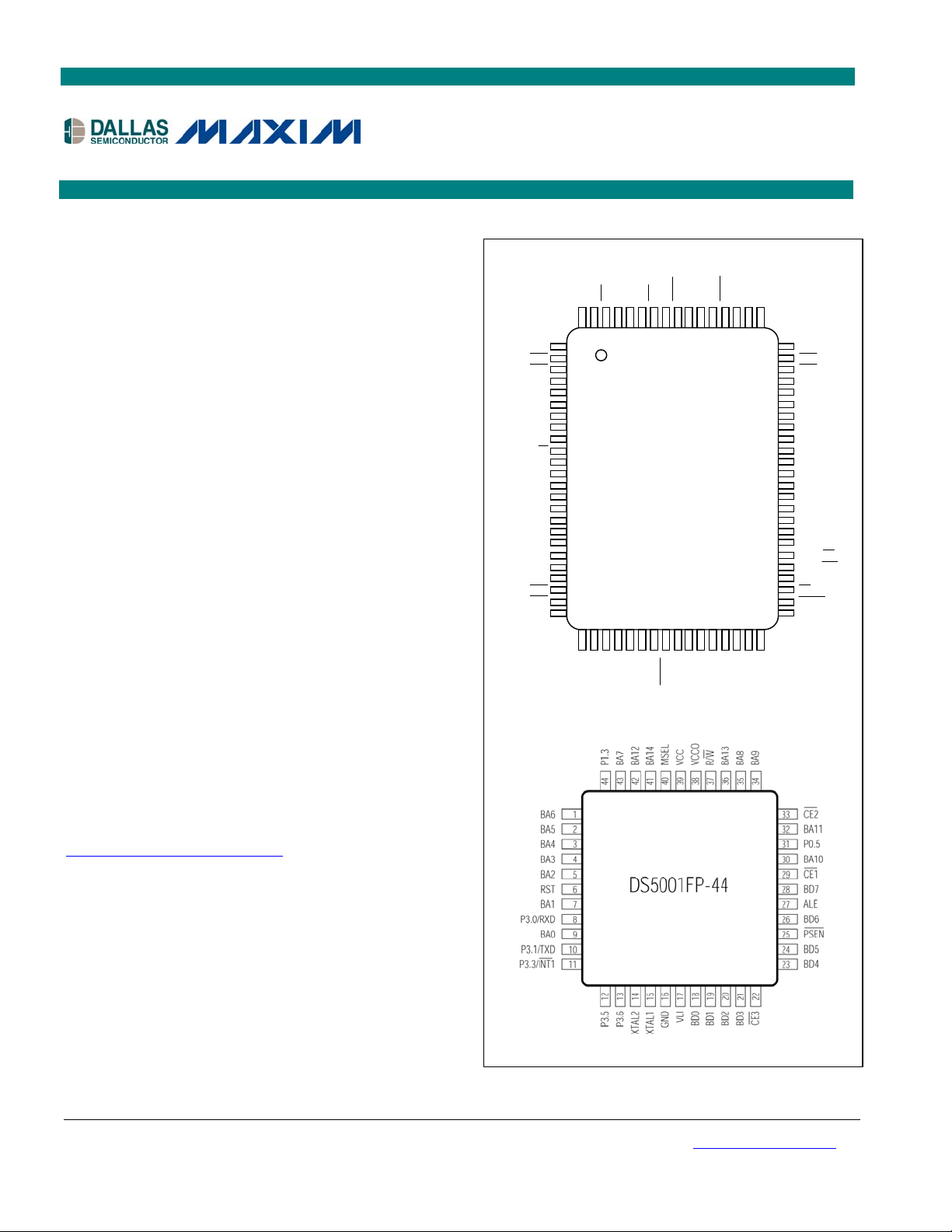
PIN CONFIGURATIONS
TOP VIEW
P0.4AD4
CE2
PE2
BA9
P0.3/AD3
BA8
P0.2/AD2
BA13
P0.1/AD1
R/W
P0.0/AD0
VCC0
VCC
MSEL
P1.0
BA14
P1.1
BA12
P1.2
BA7
P1.3
PE3
PE4
BA6
BA11
P0.5/AD5
PE1
P0.6/AD6
BA10
P0.7/AD7
CE1
N.C.
CE1N
BD7
ALE
BD6
80 79 78 77 76 75 74 73 72 71 70 69 68 67 66 65
1
2
3
4
5
6
7
8
9
10
11
12
13
14
15
16
17
18
19
20
21
22
23
24
25 26 27 28 29 30 31 32 33 34 35 36 37 38 39 40
DS5001FP
BA5
BA4
P1.4
P1.5
P1.6
BA3
P1.7
BA2
PROG
RST
BA1
P3.0/RXD
MQFP
PSEN
BD5
BA0
P3.1/TXD
P2.7/A15
BD4
64
63
62
61
60
59
58
57
56
55
54
53
52
51
50
49
48
47
46
45
44
43
42
41
P3.2/INT0
P3.3/INT1
P2.6/A14
CE3
CE4
BD3
P2.5/A13
BD2
P2.4/A12
BD1
P2.3/A11
BD0
VLI
BA15
GND
P2.2/A10
P2.1/A9
P2.0/A8
XTAL1
XTAL2
P3.7/RD
P3.6/WR
P3.5/TI
PF
VRST
P3.4/T0
MQFP
Note: Some revisions of this device may incorporate deviations from published specifications known as errata. Multiple revisions of any device
may be simultaneously available through various sales channels. For information about device errata, click here: www.maxim-ic.com/errata
1 of 27 REV: 070605
.
Page 2

DS5001FP
ORDERING INFORMATION
PART TEMP RANGE
DS5001FP-16 0°C to +70°C 16 80 MQFP
DS5001FP-16+ 0°C to +70°C 16 80 MQFP
DS5001FP-16N -40°C to +85°C 16 80 MQFP
DS5001FP-16N+ -40°C to +85°C 16 80 MQFP
DS5001FP-12-44 0°C to +70°C 12 44MQFP
DS5001FP-12-44+ 0°C to +70°C 12 44 MQFP
+ Denotes a Pb-free/RoHS-compliant device.
MAX CLOCK
SPEED (MHz)
PINPACKAGE
DESCRIPTION
The DS5001FP 128k soft microprocessor chip is an 8051-compatible microprocessor based on NV RAM
technology and designed for systems that need large quantities of nonvolatile memory. It provides full
compatibility with the 8051 instruction set, timers, serial port, and parallel I/O ports. By using NV RAM
instead of ROM, the user can program and then reprogram the microprocessor while in-system. The
application software can even change its own operation, which allows frequent software upgrades,
adaptive programs, customized systems, etc. In addition, by using NV SRAM, the DS5001FP is ideal for
data logging applications. It also connects easily to a Dallas real-time clock.
The DS5001FP provides the benefits of NV RAM without using I/O resources. It uses a nonmultiplexed
byte-wide address and data bus for memory access. This bus performs all memory access and provides
decoded chip enables for SRAM, which leaves the 32 I/O port pins free for application use. The
DS5001FP uses ordinary SRAM and battery-backs the memory contents for over 10 years at room
temperature with a small external battery. A DS5001FP also provides high-reliability operation in harsh
environments. These features include the ability to save the operating state, power-fail reset, power-fail
interrupt, and watchdog timer.
A user programs the DS5001FP through its on-chip serial bootstrap loader. The bootstrap loader
supervises the loading of software into NV RAM, validates it, and then becomes transparent to the user.
Software can be stored in multiple 32kB or one 128kB CMOS SRAM(s). Using its internal partitioning,
the DS5001FP can divide a common RAM into user-selectable program and data segments. This partition
can be selected at program loading time, but can then be modified later at any time. The microprocessor
decodes memory access to the SRAM and addresses memory through its byte-wide bus. Memory portions
designated code or ROM are automatically write-protected by the microprocessor. Combining program
and data storage in one device saves board space and cost.
The DS5001FP offers several bank switches for access to even more memory. In addition to the primary
data area of 64kB, a peripheral selector creates a second 64kB data space with four accompanying chip
enables. This area can be used for memory-mapped peripherals or more data storage. The DS5001FP can
also use its expanded bus on ports 0 and 2 (like an 8051) to access an additional 64kB of data space.
Lastly, the DS5001FP provides one additional bank switch that changes up to 60kB of the NV RAM
program space into data memory. Thus, with a small amount of logic, the DS5001 accesses up to 252kB
of data memory.
The DS2251T is available (Refer to the data sheet at www.maxim-ic.com/microcontrollers
.) for users
who want a preconstructed module using the DS5001FP, RAM, lithium cell, and a real-time clock. For
more details, refer to the Secure Microcontroller User’s Guide. For users desiring software security, the
DS5002FP is functionally identical to the DS5001FP but provides superior firmware security. The 44-pin
version of the device is functionally identical to the 80-pin version but sports a reduced pin count and
footprint.
2 of 27
Page 3
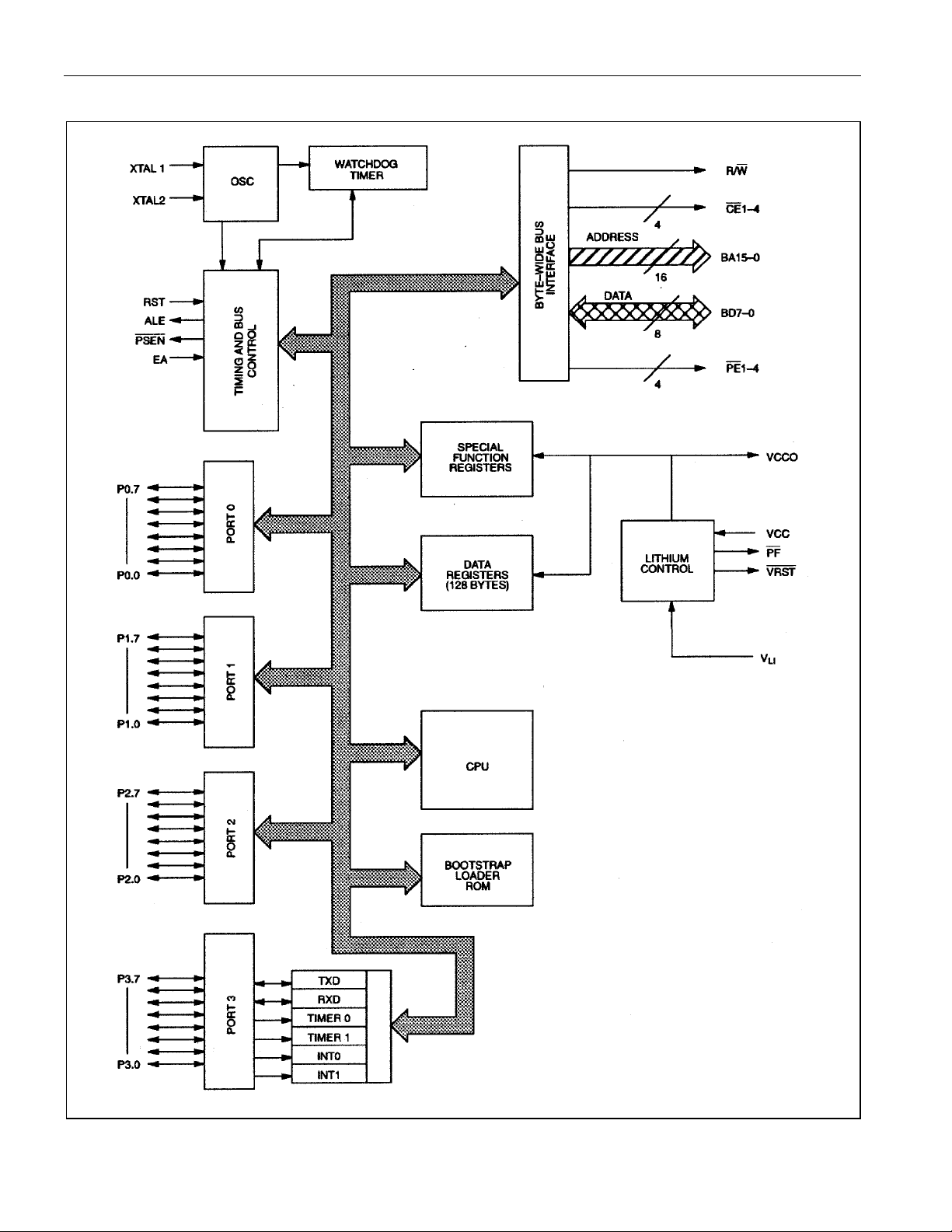
Figure 1. BLOCK DIAGRAM
DS5001FP
3 of 27
Page 4
PIN DESCRIPTION
PIN
80 PIN 44 PIN
11, 9, 7,
5, 1, 79,
77, 75
31
(P0.5)
15, 17,
19, 21,
25, 27,
44
(P1.3)
29, 31
49, 50,
51, 56,
58, 60,
—
64, 66
36 8
NAME FUNCTION
P0.0–
P0.7
P1.0–
P1.7
P2.0–
P2.7
P3.0/RX
D
DS5001FP
General-Purpose I/O Port 0. This port is open-drain and cannot drive a logic 1. It
requires external pullups. Port 0 is also the multiplexed expanded address/data bus.
When used in this mode, it does not require pullups.
General-Purpose I/O Port 1
General-Purpose I/O Port 2. Also serves as the MSB of the address in expanded
memory accesses, and as pins of the RPC mode when used.
General-Purpose I/O Port Pin 3.0. Also serves as the receive signal for the on
board UART. This pin should not be connected directly to a PC COM port.
38 10
39 —
40 11
41 —
44 12
45 13
46 —
68 25
34 6
70 27
47, 48 14, 15
52 16
P3.1/TX
D
P3.2/
INT0
P3.3/
INT1
P3.4/T0
P3.5/T1
P3.6/
P3.7/
General-Purpose I/O Port Pin 3.1. Also serves as the transmit signal for the on
board UART. This pin should not be connected directly to a PC COM port.
General-Purpose I/O Port Pin 3.2. Also serves as the active-low external interrupt
0.
General-Purpose I/O Port Pin 3.3. Also serves as the active-low external interrupt
1.
General-Purpose I/O Port Pin 3.4. Also serves as the timer 0 input.
General-Purpose I/O Port Pin 3.5. Also serves as the timer 1 input.
General-Purpose I/O Port Pin. Also serves as the write strobe for expanded bus
WR
operation.
General-Purpose I/O Port Pin. Also serves as the read strobe for expanded bus
RD
operation.
Program Store Enable. This active-low signal is used to enable an external
program memory when using the expanded bus. It is normally an output and should
PSEN
be unconnected if not used.
PSEN is pulled down externally. This should only be done once the DS5001FP
time,
is already in a reset state. The device that pulls down should be open drain since it
must not interfere with
Active-High Reset Input. A logic 1 applied to this pin will activate a reset state.
RST
This pin is pulled down internally so this pin can be left unconnected if not used. An
RC power-on reset circuit is not needed and is not recommended.
Address Latch Enable. Used to demultiplex the multiplexed expanded address/data
ALE
bus on port 0. This pin is normally connected to the clock input on a ’373 type
transparent latch.
XTAL2,
XTAL1
Crystal Connections. Used to connect an external crystal to the internal oscillator.
XTAL1 is the input to an inverting amplifier and XTAL2 is the output.
GND Logic Ground
PSEN also is used to invoke the bootstrap loader. At this
PSEN under normal operation.
13 39
12 38
54 17
V
Power Supply, +5V
CC
Output. This is switched between VCC and VLI by internal circuits based on the
V
CC
V
CCO
level of V
The lithium cell remains isolated from a load. When V
switches to the V
V
LI
Lithium Voltage Input. Connect to a lithium cell greater than V
than V
LImax
. When power is above the lithium input, power will be drawn from VCC.
CC
is below VLI, the V
source. V
LI
CC
should be connected to the VCC pin of an SRAM.
CCO
LIMIN
CCO
and no greater
as shown in the electrical specifications. Nominal value is +3V.
4 of 27
Page 5
PIN DESCRIPTION (continued)
PIN
80 PIN 44 PIN
53, 16,
8, 18,
80, 76,
4, 6, 20,
24, 26,
28, 30,
33, 35,
41, 36,
42, 32,
30, 34,
35, 43,
1, 2, 3,
4, 5, 7,
37
71, 69,
67, 65,
61, 59,
57, 55
28, 26,
24, 23,
21, 20,
19, 18
10 37
74 29
72 —
2 33
63 22
62 —
78 —
3 —
22 —
23 —
32 —
9
NAME FUNCTION
Byte-Wide Address Bus Bits 14–0. This bus is combined with the nonmultiplexed
data bus (BD7–0) to access NV SRAM. Decoding is performed using
BA14–
BA0
CE4 . Therefore, BA15 is not actually needed. Read/write access is controlled by
W . BA14–0 connect directly to an 8k, 32k, or 128k SRAM. If an 8k RAM is
R/
used, BA13 and BA14 are unconnected. If a 128k SRAM is used, the micro converts
CE2 and CE3 to serve as A16 and A15 respectively.
Byte-Wide Data Bus Bits 7–0. This 8-bit, bidirectional bus is combined with the
BD7–0
nonmultiplexed address bus (BA14–0) to access NV SRAM. Decoding is performed
on
CE1 and CE2 . Read/write access is controlled by R/ W . BD7–0 connect directly to
an SRAM, and optionally to a real-time clock or other peripheral.
Read/Write. This signal provides the write enable to the SRAMs on the byte-wide
R/
W
bus. It is controlled by the memory map and partition. The blocks selected as
program (ROM) are write-protected.
Chip Enable 1. This is the primary decoded chip enable for memory access on the
CE1
byte-wide bus. It connects to the chip enable input of one SRAM. CE1 is lithiumbacked. It remains in a logic high inactive state when V
CE1N
Non-Battery-Backed Version of Chip Enable 1. This can be used with a 32kB
EPROM. It should not be used with a battery-backed chip.
Chip Enable 2. This chip enable is provided to access a second 32k block of
CE2
memory. It connects to the chip enable input of one SRAM. When MSEL = 0, the
micro converts
remains at a logic high when V
Chip Enable 3. This chip enable is provided to access a third 32k block of memory.
CE3
It connects to the chip enable input of one SRAM. When MSEL = 0, the micro
converts
CE3 into A15 for a 128k x 8 SRAM. CE3 is lithium-backed and remains at
a logic high when V
Chip Enable 4. This chip enable is provided to access a fourth 32k block of
CE4
memory. It connects to the chip-enable input of one SRAM. When MSEL = 0, this
signal is unused.
Peripheral Enable 1. Accesses data memory between addresses 0000h and 3FFFh
when the PES bit is set to a logic 1. Commonly used to chip enable a byte-wide real-
PE1
time clock such as the DS1283.
when VCC falls below VLI. Connect PE1 to battery-backed functions only.
Peripheral Enable 2. Accesses data memory between addresses 4000h and 7FFFh
PE2
when the PES bit is set to a logic 1.
high when V
Peripheral Enable 3. Accesses data memory between addresses 8000h and BFFFh
PE3
when the PES bit is set to a logic 1.
to any type of peripheral function. If connected to a battery-backed chip, it needs
additional circuitry to maintain the chip enable in an inactive state when V
Peripheral Enable 4. Accesses data memory between addresses C000h and FFFFh
PE4
when the PES bit is set to a logic 1.
to any type of peripheral function. If connected to a battery-backed chip, it needs
additional circuitry to maintain the chip enable in an inactive state when V
Invokes the bootstrap loader on a falling edge. This signal should be debounced
PROG
so that only one edge is detected. If connected to ground, the micro enters bootstrap
loading on power-up. This signal is pulled up internally.
CE1 through
falls below VLI.
CC
CE2 into A16 for a 128k x 8 SRAM. CE2 is lithium-backed and
falls below VLI.
CC
falls below VLI.
CC
CE4 is lithium-backed and remains at a logic high when V
PE1 is lithium-backed and remains at a logic high
PE2 is lithium-backed and remains at a logic
falls below VLI. Connect PE2 to battery-backed functions only.
CC
PE3 is not lithium-backed and can be connected
PE4 is not lithium-backed and can be connected
DS5001FP
< VLI.
CC
< VLI.
CC
< VLI.
CC
5 of 27
Page 6
DS5001FP
PIN DESCRIPTION (continued)
PIN
80 PIN 44 PIN
42 —
43 —
14 40
73 —
NAME FUNCTION
This I/O pin (open drain with internal pullup) indicates that the power supply
(V
) has fallen below the V
CC
VRST
PF
MSEL
N.C. No Connection
this occurs, the DS5001FP drives this pin to a logic 0. Because the micro is lithiumbacked, this signal is guaranteed even when V
also forces a reset if pulled low externally. This allows multiple parts to synchronize
their power-down resets.
This output goes to a logic 0 to indicate that V
switched to lithium backup. Because the micro is lithium-backed, this signal is
guaranteed even when V
lithium-powered current to isolate battery-backed functions from non-battery-backed
functions.
Memory Select. This signal controls the memory size selection. When MSEL =
+5V, the DS5001FP expects to use 32k x 8 SRAMs. When MSEL = 0V, the
DS5001FP expects to use a 128k x 8 SRAM. MSEL must be connected regardless of
partition, mode, etc.
= 0V. The normal application of this signal is to control
CC
level and the micro is in a reset state. When
CCmin
= 0V. Because it is an I/O pin, it
CC
< VLI and the micro has
CC
INSTRUCTION SET
The DS5001FP executes an instruction set that is object code-compatible with the industry standard 8051
microcontroller. As a result, software development packages such as assemblers and compilers that have
been written for the 8051 are compatible with the DS5001FP. A complete description of the instruction
set and operation are provided in the Secure Microcontroller User’s Guide. Also note that the DS5001FP
is embodied in the DS2251T module. The DS2251T combines the DS5001FP with between 32k and 128k
of SRAM, a lithium cell, and a real-time clock. This is packaged in a 72-pin SIMM module.
MEMORY ORGANIZATION
Figure 2 illustrates the memory map accessed by the DS5001FP. The entire 64k of program and 64k of
data are potentially available to the byte-wide bus. This preserves the I/O ports for application use. The
user controls the portion of memory that is actually mapped to the byte-wide bus by selecting the program
range and data range. Any area not mapped into the NV RAM is reached by the expanded bus on ports 0
and 2. An alternate configuration allows dynamic partitioning of a 64k space as shown in Figure 3.
Selecting PES=1 provides another 64k of potential data storage or memory-mapped peripheral space as
shown in Figure 4. These selections are made using special function registers. The memory map and its
controls are covered in detail in the Secure Microcontroller User’s Guide.
6 of 27
Page 7
Figure 2. MEMORY MAP IN NONPARTITIONABLE MODE (PM = 1)
DS5001FP
7 of 27
Page 8
Figure 3. MEMORY MAP IN PARTITIONABLE MODE (PM = 0)
DS5001FP
NOTE: PARTITIONABLE MODE IS NOT SUPPORTED WHEN MSEL PIN = 0 (128kB MODE).
8 of 27
Page 9
Figure 4. MEMORY MAP WITH PES = 1
DS5001FP
9 of 27
Page 10

DS5001FP
Figure 5 illustrates a typical memory connection for a system using a 128kB SRAM. Note that in this
configuration, both program and data are stored in a common RAM chip Figure 6 shows a similar system
with using two 32kB SRAMs. The byte-wide address bus connects to the SRAM address lines. The
bidirectional byte-wide data bus connects the data I/O lines of the SRAM.
Figure 5. CONNECTION TO 128k x 8 SRAM
10 of 27
Page 11

Figure 6. DS5001FP CONNECTION TO 64k x 8 SRAM
DS5001FP
POWER MANAGEMENT
The DS5001FP monitors VCC to provide power-fail reset, early warning power-fail interrupt, and switch
over to lithium backup. It uses an internal bandgap reference in determining the switch points. These are
called V
interrupt vector to location 2Bh if the power-fail warning was enabled. Full processor operation continues
regardless. When power falls further to V
execution is performed unless power rises back above V
signal go to an inactive (logic 1) state. VCC is still the power source at this time. When V
to below V
disabled and the remaining nonvolatile states are retained. Any devices connected V
the lithium cell at this time. V
varies depending on the load. Low power SRAMs should be used for this reason. When using the
DS5001FP, the user must select the appropriate battery to match the RAM data retention current and the
desired backup lifetime. Note that the lithium cell is only loaded when V
more information on this topic. The trip points V
section.
, V
PFW
, internal circuitry switches to the lithium cell for power. The majority of internal circuits are
LI
, and VLI, respectively. When VCC drops below V
CCMIN
, the DS5001FP invokes a reset state. No further code
CCMIN
CCMIN
is at the lithium battery voltage minus approximately 0.45V. This drop
CCO
and V
CCMIN
, the DS5001FP performs an
PFW
. All decoded chip enables and the R/ W
drops further
CC
are powered by
CCO
< V
CC
are listed in the Electrical Specifications
PFW
. The User’s Guide has
LI
11 of 27
Page 12

DS5001FP
ABSOLUTE MAXIMUM RATINGS
Voltage Range on Any Pin Relative to Ground…………………………..…………………….-0.3V to (VCC + 0.5V)
Voltage Range on V
Related to Ground………………………………………………………………-0.3V to 6.0V
CC
Operating Temperature Range………………………………………………………………………...-40°C to +85°C
Storage Temperature Range (Note 1)………………………………………………………………..-55°C to +125°C
Soldering Temperature…………………………………………………….See IPC/JEDEC J-STD-020 Specification
This is a stress rating only and functional operation of the device at these or any other conditions above those indicated in the operation
sections of this specification is not implied. Exposure to absolute maximum rating conditions for extended periods of time may affect reliability.
Note 1: Storage temperature is defined as the temperature of the device when V
= 0V and VLI = 0V. In
CC
this state, the contents of SRAM are not battery-backed and are undefined.
DC CHARACTERISTICS
(VCC = 5V ±10%, TA = 0°C to +70°C.)
PARAMETER SYMBOL MIN TYP MAX UNITS NOTES
Input Low Voltage VIL -0.3 +0.8 V 1
Input High Voltage V
Input High Voltage
(RST, XTAL1,
PROG )
Output Low Voltage
= 1.6mA (Ports 1, 2, 3, PF )
at I
OL
Output Low Voltage
at I
= 3.2mA (Ports 0, ALE, PSEN ,
OL
BA15–0, BD7–0, R/
CE 1–4, PE 1–4, V
W , CE1N ,
)
RST
Output High Voltage
= -80µA (Ports 1, 2, 3)
at I
OH
Output High Voltage
at I
= -400µA (Ports 0, ALE, PSEN ,
OH
PF , BA15–0, BD7–0, R/ W , CE1N ,
CE 1–4, PE 1–4, V
RST
)
Input Low Current
V
= 0.45V (Ports 1, 2, 3)
IN
Transition Current; 1 to 0
V
= 2.0V (Ports 1, 2, 3)
IN
(0°C to +70°C)
Transition Current; 1 to 0
= 2.0V (Ports 1, 2, 3)
V
IN
(-40°C to +85°C)
2.0 VCC + 0.3 V 1
IH1
V
3.5 VCC + 0.3 V 1
IH2
0.15 0.45 V 1, 11
V
OL1
0.15 0.45 V 1
V
OL2
V
2.4 4.8 V 1
OH1
V
2.4 4.8 V 1
OH2
-50 µA
I
IL
ITL -500 µA
I
-600 µA 10
TL
12 of 27
Page 13

DS5001FP
DC CHARACTERISTICS (continued)
(VCC = 5V ±10%, TA = 0°C to +70°C.)
PARAMETER SYMBOL MIN TYP MAX UNITS NOTES
Input Leakage Current
0.45 < V
< VCC (Port 0, MSEL)
IN
RST Pulldown Resistor
(0°C to +70°C)
RST Pulldown Resistor
(-40°C to +85°C)
VRST Pullup Resistor
PROG Pullup Resistor
Power-Fail Warning Voltage
(0°C to +70°C)
Power-Fail Warning Voltage
(-40°C to +85°C)
Minimum Operating Voltage
(0°C to +70°C)
Minimum Operating Voltage
(-40°C to +85°C)
Operating Voltage VCC V
Lithium Supply Voltage VLI 2.5 4.0 V 1
Operating Current at 16MHz ICC 36 mA 2
Idle Mode Current at 12MHz
(0°C to +70°C)
Idle Mode Current at 12MHz
(-40°C to +85°C)
Stop Mode Current I
Pin Capacitance CIN 10 pF 5
Output Supply Voltage (V
) V
CCO
Output Supply Battery-Backed Mode
(V
, CE 1-4, PE 1-2)
CCO
(0°C to +70°C)
Output Supply Battery-Backed Mode
(V
, CE 1-4, PE 1-2)
CCO
(-40°C to +85°C)
Output Supply Current
at V
= VCC - 0.45V
CCO
Lithium-Backed Quiescent Current
(0°C to +70°C)
Lithium-Backed Quiescent Current
(-40°C to +85°C)
With BAT = 3.0V
(0°C to +70°C)
Reset Trip Point
in Stop Mode
With BAT = 3.0V
(-40°C to +85°C)
With BAT = 3.0V
(0°C to +70°C)
+10 µA
I
IL
40 150
R
RE
30 180
R
RE
R
4.7
VR
R
40
PR
4.25 4.37 4.50 V 1
V
PFW
4.1 4.37 4.6 V 1, 10
V
PFW
V
V
4.00 4.12 4.25 V 1
CCMIN
3.85 4.09 4.25 V 1, 10
CCMIN
5.5 V 1
CCMIN
7.0 mA 3
I
IDLE
8.0 mA 3, 10
I
IDLE
80 µA 4
STOP
V
CCO1
V
CCO2
V
CCO2
I
75 mA 6
CCO1
5 75 nA 7
I
LI
75 500 nA 7
I
LI
CC
-0.45
V
LI
-0.65
V
LI
-0.9
V 1, 2
V 1, 8
V 1, 8, 10
kW
kW
kW
kW
10
4.0 4.25 1
3.85 4.25 1, 10
4.4 4.65 1
13 of 27
Page 14

DS5001FP
AC CHARACTERISTICS: EXPANDED BUS MODE TIMING SPECIFICATIONS
(VCC = 5V ±10%, TA = 0°C to +70°C.)
# PARAMETER SYMBOL MIN MAX UNITS
1 Oscillator Frequency 1/ t
2 ALE Pulse Width t
3 Address Valid to ALE Low t
4 Address Hold After ALE Low t
ALE Low to Valid Instruction In
5
6
ALE Low to
7
PSEN Pulse Width
PSEN Low to Valid Instruction
8
PSEN Low
In
9
Input Instruction Hold After
10
Input Instruction Float After
11
Address Hold After
Address Valid to Valid
12
Instruction In
13
PSEN Low to Address Float
14
RD Pulse Width
15
WR Pulse Width
16
RD Low to Valid Data In
17
Data Hold After
18
Data Float After
PSEN Going High
RD High
RD High
19 ALE Low to Valid Data In
20 Valid Address to Valid Data In
at 12MHz 4t
at 16MHz
at 12MHz
at 16MHz
PSEN Going High
PSEN Going High
at 12MHz 5t
at 16MHz
at 12MHz 5t
at 16MHz
at 12MHz 8t
at 16MHz
at 12MHz 9t
at 16MHz
21
ALE Low to
22
Address Valid to
23
Data Valid to
24
Data Valid to
25
Data Valid After
26
RD Low to Address Float
27
RD or WR High to ALE High
RD or WR Low
RD or WR Low
WR Going Low
WR High
WR High
at 12MHz 7t
at 16MHz
t
1.0 16 MHz
CLK
2t
ALPW
t
AVALL
t
AVAAV
t
ALLVI
t
t
ALLPSL
t
3t
PSPW
t
PSLVI
t
0 ns
PSIV
t
t
PSIX
t
t
PSAV
t
AVVI
t
0 ns
PSLAZ
6t
t
RDPW
t
6t
WRPW
t
RDLDV
0 ns
t
RDHDV
2t
t
RDHDZ
t
ALLVD
t
AVDV
t
t
t
3t
ALLRDL
t
4t
AVRDL
t
t
DVWRL
DVWRH
t
WRHDV
0 ns
t
RDLAZ
t
RDHALH
- 40 ns
CLK
- 40 ns
CLK
- 35 ns
CLK
- 150
CLK
4t
- 25 ns
CLK
- 35 ns
CLK
3t
3t
- 8 ns
CLK
5t
- 100 ns
CLK
- 100 ns
CLK
5t
8t
9t
- 50 3t
CLK
- 130 ns
CLK
- 60 ns
CLK
- 150
CLK
7t
- 90
CLK
- 50 ns
CLK
- 40 t
CLK
- 90
CLK
- 150
CLK
- 90
CLK
- 20 ns
CLK
- 150
CLK
- 90
CLK
- 165
CLK
- 105
CLK
- 70 ns
CLK
- 150
CLK
- 90
CLK
- 165
CLK
- 105
CLK
+ 50 ns
CLK
+ 50 ns
CLK
ns
ns
ns
ns
ns
ns
ns
14 of 27
Page 15

EXPANDED PROGRAM-MEMORY READ CYCLE
DS5001FP
EXPANDED DATA-MEMORY READ CYCLE
15 of 27
Page 16

EXPANDED DATA-MEMORY WRITE CYCLE
DS5001FP
16 of 27
Page 17
DS5001FP
AC CHARACTERISTICS: EXTERNAL CLOCK DRIVE
(VCC = 5V ±10%, TA = 0°C to +70°C.)
# PARAMETER SYMBOL MIN MAX UNITS
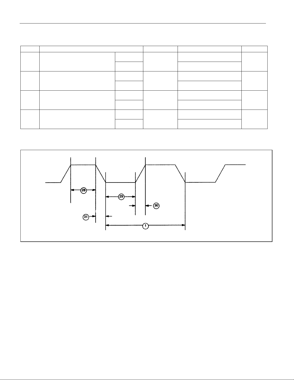
28 External Clock-High Time
at 12MHz 20
t
at 16MHz
CLKHPW
15
ns
29 External Clock-Low Time
30 External Clock-Rise Time
31 External Clock-Fall Time
EXTERNAL CLOCK TIMING
at 12MHz 20
t
at 16MHz
CLKLPW
15
at 12MHz 20
t
at 16MHz
CLKR
15
at 12MHz 20
t
at 16MHz
CLKF
15
ns
ns
ns
17 of 27
Page 18

DS5001FP
AC CHARACTERISTICS: POWER CYCLE TIME
(VCC = 5V ±10%, TA = 0°C to +70°C.)
# PARAMETER SYMBOL MIN MAX UNITS
32 Slew Rate from V
33 Crystal Startup Time t
34 Power-On Reset Delay t
to VLI t
CCMIN
130 µs
F
(Note 9)
CSU
21,504 t
POR
CLK
POWER CYCLE TIMING
18 of 27
Page 19

DS5001FP
AC CHARACTERISTICS: SERIAL PORT TIMING—MODE 0
(VCC = 5V ±10%, TA = 0°C to +70°C.)
# PARAMETER SYMBOL MIN MAX UNITS
35 Serial-Port Clock-Cycle Time t
36 Output-Data Setup to Rising-Clock Edge t
12t
SPCLK
10t
DOCH
µs
CLK
- 133 ns
CLK
37 Output-Data Hold After Rising-Clock Edge t
38 Clock-Rising Edge to Input-Data Valid t
39 Input-Data Hold After Rising-Clock Edge t
SERIAL PORT TIMING—MODE 0
2t
CHDO
10t
CHDV
0 ns
CHDIV
- 117 ns
CLK
- 133 ns
CLK
19 of 27
Page 20

DS5001FP
AC CHARACTERISTICS: BYTE-WIDE ADDRESS/DATA BUS TIMING
(VCC = 5V ±10%, TA = 0°C to +70°C.)
# PARAMETER SYMBOL MIN MAX UNITS
40
41
Delay to Byte-Wide Address Valid from
CE1 , CE2 , or CE1N Low During Op Code Fetch
Pulse Width of
CE 1-4, PE 1-4 or CE1N
t
30 ns
CE1LPA
t
CEPW
4t
- 35 ns
CLK
42
43
44
45
46
47
48
49
50
51
Byte-Wide Address Hold After
CE1N High During Op Code Fetch
Byte-Wide Data Setup to
CE1 , CE2 , or
CE1 , CE2 , or CE1N
High During Op Code Fetch
Byte-Wide Data Hold After
CE1 , CE2 or CE1N
High During Op Code Fetch
Byte-Wide Address Hold After
PE 1-4, or CE1N High During MOVX
CE 1-4,
Delay from Byte-Wide Address Valid
CE 1-4, PE 1-4, or CE1N Low During MOVX
Byte-Wide Data Setup to
CE1N High During MOVX (read)
Byte-Wide Data Hold After
PE 1-4, or CE1N High During MOVX (read)
Byte-Wide Address Valid to R/
CE 1-4, PE 1-4, or
CE 1-4,
W Active
During MOVX (write)
Delay from R/
W Low to Valid Data Out
During MOVX (write)
Valid Data-Out Hold Time from
PE 1-4, or CE1N High
CE 1-4,
2t
t
CE1HPA
t
t
1t
OVCE1H
0 ns
CE1HOV
t
4t
CEHDA
t
4t
CELDA
t
1t
DACEH
0 ns
t
CEHDV
t
3t
AVRWL
t
20 ns
RWLDV
t
1t
CEHDV
- 20 ns
CLK
+ 40 ns
CLK
- 30 ns
CLK
- 35 ns
CLK
+ 40 ns
CLK
- 35 ns
CLK
- 15 ns
CLK
52
53
Valid Data-Out Hold Time from R/
Write Pulse Width (R/
W Low Time)
W High
20 of 27
t
0 ns
RWHDV
t
RWLPW
6t
- 20 ns
CLK
Page 21

BYTE-WIDE BUS TIMING
DS5001FP
RPC AC CHARACTERISTICS: DBB READ
(VCC = 5V ±10%, TA = 0°C to +70°C.)
# PARAMETER SYMBOL MIN MAX UNITS
54
55
56
57
58
59
CS , A
CS , A
RD Pulse Width
CS , A
RD to Data-Out Delay
RD to Data-Float Delay
Setup to RD
0
Hold After RD
0
to Data-Out Delay
0
0 ns
t
AR
0 ns
t
RA
tRR 160 ns
130 ns
t
AD
tRD 0 130 ns
t
85 ns
RDZ
RPC AC CHARACTERISTICS: DBB WRITE
(VCC = 5V ±10%, TA = 0°C to +70°C.)
# PARAMETER SYMBOL MIN MAX UNITS
60
61A
61B
62
63
64
CS , A
CS , Hold After WR
A
WR Pulse Width
Data Setup to
Data Hold After
Setup to WR
0
, Hold After WR
0
WR
WR
0 ns
t
AW
0 ns
t
WA
20 ns
t
WA
160 ns
t
WW
130 ns
t
DW
20 ns
t
WD
21 of 27
Page 22

DS5001FP
AC CHARACTERISTICS: DMA
(VCC = 5V ±10%, TA = 0°C to +70°C.)
# PARAMETER SYMBOL MIN MAX UNITS
65
66
67
68
DACK to WR or RD
RD or WR to DACK
DACK to Data Valid
RD or WR to DRQ Cleared
0 ns
t
ACC
0 ns
t
CAC
0 130 ns
t
ACD
110 ns
t
CRQ
AC CHARACTERISTICS: PROG
(VCC = 5V ±10%, TA = 0°C to +70°C.)
# PARAMETER SYMBOL MIN MAX UNITS
69
70
PROG Low to Active
PROG High to Inactive
48 CLKS
t
PRA
48 CLKS
t
PRI
22 of 27
Page 23

RPC TIMING MODE
DS5001FP
23 of 27
Page 24

DS5001FP
NOTES:
All parameters apply to both commercial and industrial temperature operation unless otherwise noted.
1) All voltages are referenced to ground.
2) Maximum operating ICC is measured with all output pins disconnected; XTAL1 driven with t
= 10ns, VIL = 0.5V; XTAL2 disconnected; RST = PORT0 = VCC, MSEL = VSS.
t
CLKF
3) Idle mode, I
t
= 10ns, VIL = 0.5V; XTAL2 disconnected; PORT0 = VCC, RST = MSEL = VSS.
CLKF
4) Stop mode, I
, is measured with all output pins disconnected; XTAL1 driven with t
IDLE
, is measured with all output pins disconnected; PORT0 = VCC; XTAL2 not
STOP
connected; RST = MSEL = XTAL1 = VSS.
5) Pin capacitance is measured with a test frequency: 1MHz, TA = +25°C.
6) I
7) ILI is the current drawn from VLI input when VCC = 0V and V
8) V
is the maximum average operating current that can be drawn from V
CCO1
CCO
is measured with VCC < VLI, and a maximum load of 10µA on V
CCO2
in normal operation.
CCO
is disconnected.
.
CCO
9) Crystal startup time is the time required to get the mass of the crystal into vibrational motion from the
time that power is first applied to the circuit until the first clock pulse is produced by the on-chip
oscillator. The user should check with the crystal vendor for a worst-case specification on this time.
10) This parameter applies to industrial temperature operation.
11) PF pin operation is specified with V
³ 3.0V.
BAT
CLKR
CLKR
,
,
24 of 27
Page 25

DS5001FP
PACKAGE INFORMATION
(The package drawing(s) in this data sheet may not reflect the most current specifications. For the latest package outline
information, go to www.maxim-ic.com/DallasPackInfo
.)
80-PIN MQFP
DIM
A
A1
A2
B
C
D
D1
E
E1
e
L
56-G4005-001
MIN MAX
0.25 -
2.55 2.87
0.30 0.50
0.13 0.23
23.70 24.10
19.90 20.10
17.70 18.10
13.90 14.10
0.65 0.95
MM
- 3.40
0.80 BSC
25 of 27
Page 26

44-PIN MQFP
DS5001FP
26 of 27
Page 27

DS5001FP
REVISION HISTORY
The following represent the key differences between the 112795 and 073096 version of the DS5001FP
data sheet. Please review this summary carefully.
1) Change V
2) Update mechanical specifications.
The following represent the key differences between the 073096 and 111996 version of the DS5001FP
data sheet. Please review this summary carefully.
1) Change V
The following represent the key differences between the 111996 and 061297 version of the DS5001FP
data sheet. Please review this summary carefully.
specification from VLI - 0.5 to VLI - 0.65 (PCN F62501).
CC02
from VCC - 0.3 to VCC - 0.35.
CC01
1) PF signal moved from V
test specification to V
OL2
. PCN No. (D72502)
OL1
2) AC characteristics for battery-backed SDI pulse specification added.
The following represent the key differences between the 061297 and 051099 version of the DS5001FP
data sheet. Please review this summary carefully.
1) Reduced absolute maximum voltage to VCC + 0.5V.
2) Added note clarifying storage temperature specification is for non-battery-backed state.
3) Changed RRE min (industrial temp range) from 40kW to 30kW.
4) Changed V
max (industrial temp range) from 4.5V to 4.6V.
PFW
5) Added industrial specification for ILI.
6) Reduced t
CE1HOV
and t
from 10ns to 0ns.
CEHDV
The following represent the key differences between the 051099 and 052499 version of the DS5001FP
data sheet. Please review this summary carefully.
1) Minor markups and ready for approval.
The following represent the key differences between the 052499 and 052302 version of the DS5001FP
data sheet. Please review this summary carefully.
1) Added information relating to 44-pin package.
2) Updated V
CCO1
and I
specifications to reflect 0.45V internal voltage drop instead of 0.35V.
CCO1
The following represent the key differences between the 052302 and 070605 version of the DS5001FP
data sheet. Please review this summary carefully.
1) Added Pb-free part to Ordering Information table.
2) Added operating voltage specification. (This is not a new specification because operating voltage is
implied in the testing limits, but rather a clarification.)
3) Updated Absolute Maximum Ratings soldering temperature to reference JEDEC standard.
27 of 27
Maxim/Dallas Semiconductor cannot assume responsibility for use of any circuitry other than circuitry entirely embodied in a Maxim/Dallas Semiconductor product.
No circuit patent licenses are implied. Maxim/Dallas Semiconductor reserves the right to change the circuitry and specifications without notice at any time.
Maxim Integrated Products, 120 San Gabriel Drive, Sunnyvale, CA 94086 408-737-7600
The Maxim logo is a registered trademark of Maxim Integrated Products, Inc. The Dallas logo is a registered trademark of Dallas Semiconductor Corporation.
© 2005 Maxim Integrated Products · Printed USA
 Loading...