

Page 1
General Description
The DS4125, DS4150, DS4155, DS4156, DS4160,
DS4250, DS4300, DS4311, DS4312, DS4622, and
DS4776 ceramic surface-mount crystal oscillators are
part of Maxim’s DS4-XO series of crystal oscillators.
These devices offer output frequencies at 125MHz,
155.52MHz, 156.25MHz, 160MHz, 311.04MHz, 312.5MHz,
622.08MHz, and 77.76MHz. The clock oscillators are
suited for systems with tight tolerances because of the
jitter, phase noise, and stability performance. The small
package provides a format made for applications
where PCB space is critical.
These clock oscillators are crystal based and use a fundamental crystal with PLL technology to provide the
final output frequencies. Each device is offered with
LVDS or LVPECL output types. The output enable pin is
active-high logic.
These clock oscillators have very low phase jitter and
phase noise. Typical phase jitter is < 0.7ps
RMS
from
12kHz to 20MHz. The devices are designed to operate
with a 3.3V ±5% supply voltage, and are available in a
5.0mm x 3.2mm x 1.49mm, 10-pin LCCC surface-mount
ceramic package.
Applications
InfiniBand
BPON/GPON
Ethernet
10GbE
SONET/SDH
Features
♦ < 0.7ps
RMS
from 12kHz to 20MHz Jitter
♦ LVDS or LVPECL Output Types
♦ 3.3V Operating Voltage
♦ 5.0mm x 3.2mm x 1.49mm, 10-Pin LCCC Ceramic
Package
♦ -40°C to +85°C Operating Temperature Range
♦ Lead-Free/RoHS Compliant
DS4125–DS4776
DS4-XO Series Crystal Oscillators
________________________________________________________________
Maxim Integrated Products
1
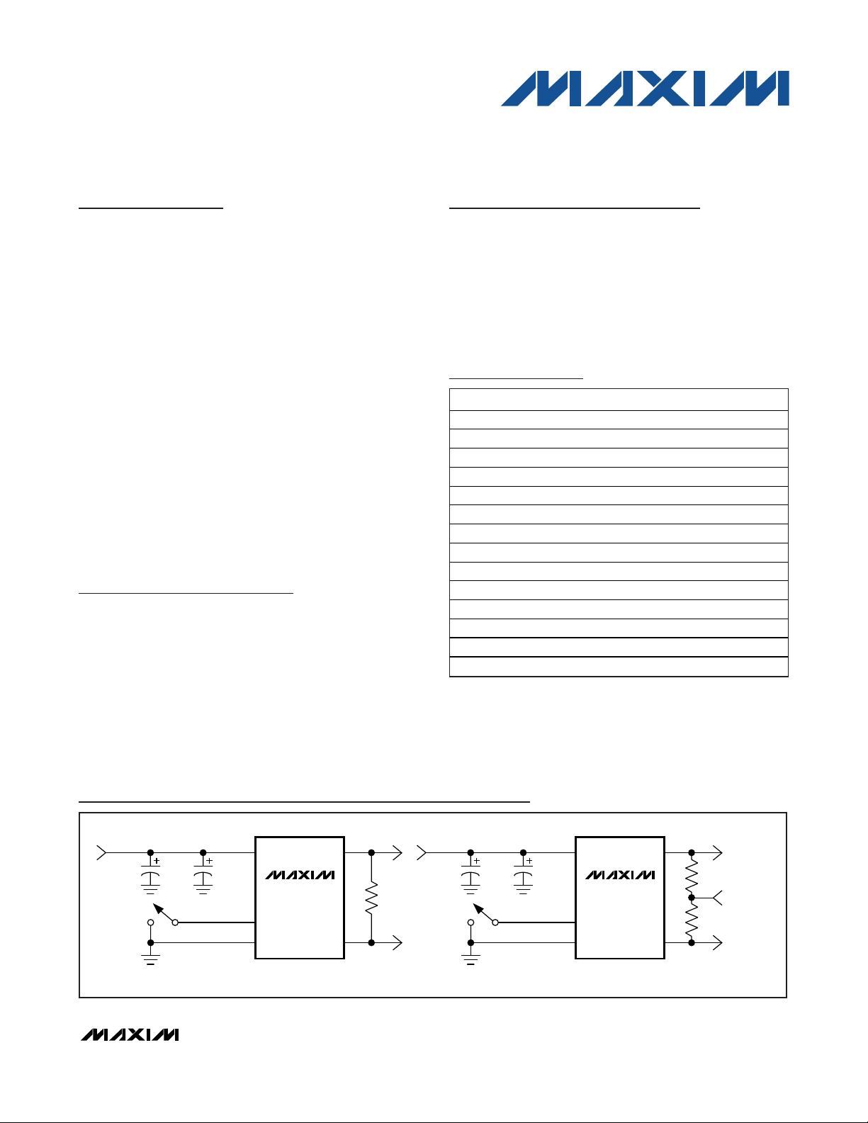
Typical Operating Circuits
Rev 2; 6/08
For pricing, delivery, and ordering information, please contact Maxim Direct at 1-888-629-4642,
or visit Maxim’s website at www.maxim-ic.com.
Pin Configuration and Selector Guide appear at end of
data sheet.
Ordering Information continued at end of data sheet.
+
Denotes a lead(Pb)-free/RoHS-compliant package. The lead
finish is JESD97 category e4 (Au over Ni) and is compatible with
both lead-based and lead-free soldering processes.
Ordering Information
PART TEMP RANGE PIN-PACKAGE
DS4125D+ -40°C to +85°C 10 LCCC
DS4125P+ -40°C to +85°C 10 LCCC
DS4150D+ -40°C to +85°C 10 LCCC
DS4150P+ -40°C to +85°C 10 LCCC
DS4155D+ -40°C to +85°C 10 LCCC
DS4155P+ -40°C to +85°C 10 LCCC
DS4156D+ -40°C to +85°C 10 LCCC
DS4156P+ -40°C to +85°C 10 LCCC
DS4160D+ -40°C to +85°C 10 LCCC
DS4160P+ -40°C to +85°C 10 LCCC
DS4250D+ -40°C to +85°C 10 LCCC
DS4250P+ -40°C to +85°C 10 LCCC
DS4300D+ -40°C to +85°C 10 LCCC
DS4300P+ -40°C to +85°C 10 LCCC
V
CC
0.1μF
0.01μF
DS4125–DS4776
OE
GND
LVDS OPTION
OUTP
OUTN
100Ω
0.1μF
0.01μF
V
CC
DS4125–DS4776
OE
GND
LVPECL OPTION
OUTP
OUTN
50Ω
50Ω
PECL_BIAS
- 2.0V
V
CC
Page 2
DS4125–DS4776
2 _______________________________________________________________________________________
ABSOLUTE MAXIMUM RATINGS
ELECTRICAL CHARACTERISTICS
(VCC= 3.135V to 3.465V, TA= -40°C to +85°C, unless otherwise noted.)
Stresses beyond those listed under “Absolute Maximum Ratings” may cause permanent damage to the device. These are stress ratings only, and functional
operation of the device at these or any other conditions beyond those indicated in the operational sections of the specifications is not implied. Exposure to
absolute maximum rating conditions for extended periods may affect device reliability.
Power-Supply Voltage (VCC) .......................................-0.3V, +4V
Operating Temperature Range ...........................-40°C to +85°C
Junction Temperature......................................................+150°C
Storage Temperature Range ...............................-55°C to +85°C
Soldering Temperature Profile
(3 passes max of reflow) ......................Refer to the IPC/JEDEC
J-STD-020 Specification.
DS4-XO Series Crystal Oscillators
PARAMETER SYMBOL CONDITIONS MIN TYP MAX UNITS
Operating Voltage Range VCC (Note 1) 3.135 3.3 3.465 V
Operating Current
Output Frequency f
Oscillator Startup Time t
Frequency Stability f
Frequency Stability O ver
Temperature with Initial Tolerance
Initial Tolerance f
Frequency Change Due to V
Frequency Change Due to Load
Variation
Aging (15 Years) f
Jitter J
Input-Voltage High (OE) VIH (Note 1)
Input-Voltage Low (OE) VIL (Note 1) 0
Input Leakage (OE) I
CC
I
LVDS, output loaded or unloaded 52 75
CC_D
I
LVPECL, output unloaded 49 70
CC_PU
LVPECL, output l oad 50 at VCC - 2.0V 74 100
I
CC_P I
f
OUT
STARTUP
f
(Note 2) 50 ms
TOTAL
f
TEMP
INITIAL
f
VCC
LOAD
AGING
RMS
LEAK
Over temperature range, aging, load,
supply, and initial tolerance (Note 3)
VCC = 3.3V -35 +35 ppm
VCC = 3.3V, TA = +25°C ±20 ppm
VCC = 3.3V ±5% -3 +3 ppm/V
±10% variation in termination
resistance
-7 +7 ppm
Integrated phase RMS; 12kHz to 5MHz,
= 3.3V, TA = +25°C
V
CC
Integrated phase RMS; 12kHz to 20MHz,
= 3.3V, TA = +25°C
V
CC
Integrated phase RMS; 12kHz to 80MHz,
= 3.3V, TA = +25°C
V
CC
GND OE VCC -50 +5.0 μA
MHz
NOM
-50 f
±1 ppm
0.7
0.7
1.0
0.7 x
V
CC
+50 ppm
NOM
VCC V
0.3 x
V
CC
mA
ps
V
Page 3
DS4125–DS4776
_______________________________________________________________________________________ 3
ELECTRICAL CHARACTERISTICS (continued)
(VCC= 3.135V to 3.465V, TA= -40°C to +85°C, unless otherwise noted.)
Note 1: All voltages referenced to ground.
Note 2: AC parameters are guaranteed by design and not production tested.
Note 3: Frequency stability is calculated as: Δf
TOTAL
= Δf
TEMP
+ Δf
VCC
x (3.3 x 5%) + Δf
LOAD
+ Δf
AGING
.
DS4-XO Series Crystal Oscillators
PARAMETER SYMBOL CONDITIONS MIN TYP MAX UNITS
LVDS
Output High Voltage V
Output Low Voltage V
Differential Output Voltage
Output Common-Mode Voltage
Variation
Change in Differential Magnitude
or Complementary Inputs
Offset Output Voltage V
Differential Output Impedance R
Output Current
OHLVDSO
OLLVDSO
|
V
ODLVDSO
V
LVDSOCOM
|V
ODLVDSO
OFFLVDS O
OLVDS O
L
VS SLVDS O
L
Output Rise Time (Different ia l) t
Output Fall T ime (Differential) t
Duty Cycle D
RLVDS O
FLVDSO
CYCLE_LVDS
Propagation Delay from OE Going
LOW to Logical 1 at OUTP
Propagation Delay from OE Going
HIGH to Output Acti ve
LVPECL
Output High Voltage V
Output Low Voltage V
Differential Voltage V
Rise Time t
Fal l Time t
Duty Cycle D
DIFF_PECL
R-PECL
F-PECL
CYCLE_PECL
Propagation Delay from OE Going
LOW to Output High Impedance
Propagation Delay from OE Going
HIGH to Output Acti ve
100 differential load (Note 1) 1.475 V
100 differential load (Note 1) 0.925 V
|
100 differential load 250 425 mV
100 differential load 150 mV
|
100 differential load 25 mV
100 differential load (Note 1) 1.125 1.275 V
80 140
OUTN or OUTP shorted to ground and
measure the current in the shorting path
OUTN or OUTP shorted together 6.5
LVDSO
40
20% to 80% 175 ps
80% to 20% 175 ps
45 55 %
t
200 ns
PA1
200 ns
t
P1A
OH
OL
Output connected to 50 at PECL_BIAS
at V
- 2.0V
CC
Output connected to 50 at PECL_BIAS
at V
- 2.0V
CC
Output connected to 50 at PECL_BIAS
at V
- 2.0V
CC
-
V
CC
1.085
-
V
CC
1.825
VCC -
0.88
V
-
CC
1.62
0.595 0.710 V
200 ps
200 ps
45 55 %
t
200 ns
PAZ
t
200 ns
PZA
mA
V
V
Page 4

Pin Description
DS4125–DS4776
DS4-XO Series Crystal Oscillators
4 _______________________________________________________________________________________
SINGLE-SIDEBAND PHASE NOISE AT fO= f
NOM
Typical Operating Characteristics
(VCC= +3.3V, TA = +25°C, unless otherwise noted.)
FREQUENCY vs. TEMPERATURE
DS4125/776 toc01
TEMPERATURE (°C)
f
OUT
DEVIATION (ppm)
806020 400-20
-18
-15
-13
-10
-8
-5
-3
0
3
5
8
10
13
15
-20
-40
OPERATING CURRENT (DS4155)
vs. OPERATING VOLTAGE
DS4125/776 toc02
VCC (V)
I
CC
(mA)
3.4353.3853.3353.2853.2353.185
48
50
53
55
45
3.135
+85°C
0°C
-40°C
+70°C
+40°C
+25°C
fM =
77.76MHz 125.00MHz 155.52MHz 156.25MHz 160.00MHz 311.04MHz 312.5MHz 622.08MHz
SINGLE-SIDEBAND PHASE NOISE AT fO = f
NOM
(dBc/Hz)
10Hz -60 -70 -70 -70 -70 -65 -65 -60
100Hz -95 -100 -100 -100 -100 -95 -95 -90
1kH z -122 -120 -120 -120 -120 -113 -113 -107
10kHz -126 -120 -120 -120 -120 -113 -113 -107
100kHz -131 -125 -125 -125 -125 -118 -118 -113
1MHz -143 -142 -142 -142 -142 -137 -137 -131
10MHz -149 -149 -149 -149 -149 -149 -149 -147
20MHz -153 -153 -153 -153 -153 -153 -153 -150
PIN NAME FUNCTION
1 OE Active-High Output Enable. Has an internal pul lup 100 k resistor.
2, 7–10 N.C. No Connection. Must be floated.
3 GND Ground
4 OUTP Posit ive Output for LVPECL or LVDS
5 OUTN Negat ive Output for LVPECL or LVDS
6 VCC Supply Voltage
— EP Exposed Paddle. Do not connect this pad or place exposed metal under the pad.
Page 5

DS4125–DS4776
DS4-XO Series Crystal Oscillators
_______________________________________________________________________________________ 5
Detailed Description
The devices consist of a fundamental-mode, AT-cut
crystal and a synthesizer IC that can synthesize any
one of these frequencies: 77.76MHz, 125MHz,
150MHz, 155.52MHz, 156.25MHz, 160MHz, 250MHz,
300MHz, 311.04MHz, 312.5MHz, and 622.08MHz.
All devices support two types of differential output drivers: LVDS and LVPECL. When the OE signal is low,
LVPECL outputs go to the PECL_BIAS level of
V
CC
- 2.0V, while the LVDS outputs are a logical one.
See Figures 2 and 3 for an LVDS and LVPECL output
timing diagram.
Additional Information
For more available frequencies, refer to the DS4106
data sheet at www.maxim-ic.com/DS4106.
Figure 1. Functional Diagram
Figure 2. LVDS Output Timing Diagram When OE Is Enabled
and Disabled
Figure 3. LVPECL Output Timing Diagram When OE Is Enabled
and Disabled
X1
TRI-
X2
DS4125–DS4776
STATE
PHASE
DET
FILTER
/m
V
CC
LC-VCO
/n
OUTSELN
OUTDRV
GND
OE
OUTP
OUTN
0.7 x V
OUTP
OUTN
CC
OE
t
P1A
0.3 x V
t
PA1
CC
0.7 x V
CC
OE
OUTP
OUTN
t
PZA
PECL_BIAS PECL_BIAS
PECL_BIAS PECL_BIAS
0.3 x V
t
PAZ
CC
Page 6

DS4125–DS4776
DS4-XO Series Crystal Oscillators
6 _______________________________________________________________________________________
Chip Information
SUBSTRATE CONNECTED TO GROUND
PROCESS: BiPOLAR SiGe
Selector Guide
+
Denotes a lead(Pb)-free/RoHS-compliant package. The lead finish is JESD97 category e4 (Au over Ni) and is compatible with both
lead-based and lead-free soldering processes.
Thermal Information
+
Denotes a lead(Pb)-free/RoHS-compliant package. The lead
finish is JESD97 category e4 (Au over Ni) and is compatible with
both lead-based and lead-free soldering processes.
Ordering Information (continued)
PART TEMP RANGE PIN-PACKAGE
DS4311D+ -40°C to +85°C 10 LCCC
DS4311P+ -40°C to +85°C 10 LCCC
DS4312D+ -40°C to +85°C 10 LCCC
DS4312P+ -40°C to +85°C 10 LCCC
DS4622D+ -40°C to +85°C 10 LCCC
DS4622P+ -40°C to +85°C 10 LCCC
DS4776D+ -40°C to +85°C 10 LCCC
DS4776P+ -40°C to +85°C 10 LCCC
THETA-JA (°C/W)
90
PART
DS4125D+ 125.00 ±50 LVDS 25D
DS4125P+ 125.00 ±50 LVPECL 25P
DS4150D+ 150.00 ±50 LVDS 50D
DS4150P+ 150.00 ±50 LVPECL 50P
DS4155D+ 155.52 ±50 LVDS 55D
DS4155P+ 155.52 ±50 LVPECL 55P
DS4156D+ 156.25 ±50 LVDS 56D
DS4156P+ 156.25 ±50 LVPECL 56P
DS4160D+ 160.00 ±50 LVDS 60D
DS4160P+ 160.00 ±50 LVPECL 60P
DS4250D+ 250.00 ±50 LVDS T5D
DS4250P+ 250.00 ±50 LVPECL T5P
DS4300D+ 300.00 ±50 LVDS 30D
DS4300P+ 300.00 ±50 LVPECL 30P
DS4311D+ 311.04 ±50 LVDS 31D
DS4311P+ 311.04 ±50 LVPECL 31P
DS4312D+ 312.50 ±50 LVDS 32D
DS4312P+ 312.50 ±50 LVPECL 32P
DS4622D+ 622.08 ±50 LVDS 62D
DS4622P+ 622.08 ±50 LVPECL 62P
DS4776D+ 77.76 ±50 LVDS 76D
DS4776P+ 77.76 ±50 LVPECL 76P
FREQUENCY (NOM)
(MHz)
FREQUENCY
STABILITY (ppm)
OUTPUT TYPE TOP MARK
Page 7

DS4125–DS4776
DS4-XO Series Crystal Oscillators
_______________________________________________________________________________________ 7
Pin Configuration
PACKAGE TYPE PACKAGE CODE DOCUMENT NO.
10 LCCC L1053+H2
21-0389
Package Information
For the latest package outline information and land patterns, go
to www.maxim-ic.com/packages
.
TOP VIEW
OE
N.C.
GND
(5.00mm × 3.20mm × 1.49mm)
*EXPOSED PAD
N.C. N.C.
+
1
2
3
*EP
N.C. N.C.
DS4125
6
V
CC
5
OUTN
4
OUTP
Page 8

DS4125–DS4776
DS4-XO Series Crystal Oscillators
Maxim cannot assume responsibility for use of any circuitry other than circuitry entirely embodied in a Maxim product. No circuit patent licenses are
implied. Maxim reserves the right to change the circuitry and specifications without notice at any time.
8
_____________________Maxim Integrated Products, 120 San Gabriel Drive, Sunnyvale, CA 94086 408-737-7600
© 2008 Maxim Integrated Products Maxim is a registered trademark of Maxim Integrated Products, Inc.
Revision History
REVISION
NUMBER
0 7/07 Initial release. —
REVISION
DATE
DESCRIPTION
Added DS4150, DS4250, DS4300. All
PAGES
CHANGED
1 3/08
2 6/08 Remo ved future status from the DS4150, DS4250, and DS4300. 1, 6
Removed f
In the Pin Description, changed the EP description to indicate that it should not
be connected and to avoid placing exposed metal under the pad location.
from the frequency stability calculation in Note 3. 3
INITIAL
4
 Loading...