

Page 1
General Description
The DS4625 is a dual-output, low-jitter clock oscillator
capable of producing frequency output pair combinations ranging from 100MHz to 625MHz. The device
combines an AT-cut crystal, an oscillator, and a lownoise phase-locked loop (PLL) in a 5.0mm x 3.2mm
surface-mount LCCC package. Standard frequency
options are listed in the
Ordering Information/Selector
Guide
table. For custom frequency options, contact the
factory at: Custom.Oscillators@maxim-ic.com
.
The DS4625 provides dual, low-voltage, positive emitter-coupled logic (LVPECL) clock output drivers. The
output drivers can be enabled and disabled through
the OE pin, which is an active-high CMOS input that
has an internal pullup resistor. When high, both output
pairs are enabled.
The device operates from a single +3.3V ±10% supply.
The operating temperature range is -40°C to +85°C.
Applications
XGMII Clock Oscillator
InfiniBand
TM/SM
SAS/SATA
PCIe
®
1GbE/10GbE
Features
♦ Standard Clock Output Frequencies: 100MHz,
125MHz, 150MHz, 156.25MHz, and 200MHz
♦ Phase Jitter < 0.7ps RMS (typical) from 12kHz to
20MHz
♦ LVPECL Output
♦ +3.3V ±10% Operating Voltage
♦ -40°C to +85°C Temperature Range
♦ Excellent Power-Supply Noise Rejection
♦ 5.0mm x 3.2mm Ceramic LCCC Package
♦ Output Enable/Disable
DS4625
3.3V Dual-Output LVPECL Clock Oscillator
________________________________________________________________
Maxim Integrated Products
1
Ordering Information/Selector Guide
19-4558; Rev 1; 3/10
For pricing, delivery, and ordering information, please contact Maxim Direct at 1-888-629-4642,
or visit Maxim’s website at www.maxim-ic.com.
+
Denotes a lead(Pb)-free/RoHS-compliant package. The lead finish is JESD97 category e4 (Au over Ni) and is compatible with both
lead-based and lead-free soldering processes.
*
Standard frequency options. Contact the factory at Custom.Oscillators@maxim-ic.com for custom frequencies.
PART TEMP RANGE
FREQUENCY (OP1:ON1)
(MHz) (f
C
)*
FREQUENCY (OP2:ON2)
(MHz) (fC)*
PIN-PACKAGE
TOP
MARK
DS4625P+100/100 -40°C to +85°C 100.000 100.000 10 LCCC 6AA
DS4625P+100/150 -40°C to +85°C 100.000 150.000 10 LCCC 6AC
DS4625P+125/125 -40°C to +85°C 125.000 125.000 10 LCCC 6BB
DS4625P+125/156 -40°C to +85°C 125.000 156.250 10 LCCC 6BD
DS4625P+150/150 -40°C to +85°C 150.000 150.000 10 LCCC 6CC
DS4625P+150/200 -40°C to +85°C 150.000 200.000 10 LCCC 6CE
Pin Configuration and Typical Application Circuit appear at end of data sheet.
InfiniBand is a trademark and service mark of the InfiniBand Trade Association.
PCIe is a registered trademark of PCI-SIG Corp.
Page 2
DS4625
3.3V Dual-Output LVPECL Clock Oscillator
2 _______________________________________________________________________________________
ABSOLUTE MAXIMUM RATINGS
RECOMMENDED OPERATING CONDITIONS
Stresses beyond those listed under “Absolute Maximum Ratings” may cause permanent damage to the device. These are stress ratings only, and functional
operation of the device at these or any other conditions beyond those indicated in the operational sections of the specifications is not implied. Exposure to
absolute maximum rating conditions for extended periods may affect device reliability.
(All voltages referenced to ground unless otherwise noted.)
Voltage Range on Any Pin Relative to Ground......-0.3V to +4.0V
Operating Temperature Range ...........................-40°C to +85°C
Junction Temperature......................................................+150°C
θJA...................................................................+90°C/W (Note 1)
Storage Temperature Range ...............................-55°C to +85°C
Lead Temperature (soldering, 10s) .................................+260°C
Soldering Temperature (reflow) .......................................+260°C
ELECTRICAL CHARACTERISTICS
(VCC= +2.97V to +3.63V, TA= -40°C to +85°C, typical values are at VCC= +3.3V and TA= +25°C, unless otherwise noted.) (Notes 2, 3)
Note 1: Package thermal resistances were obtained using a two-layer board. For detailed information on package thermal consider-
ations, refer to www.maxim-ic.com/thermal-tutorial
.
PARAMETER SYMBOL CONDITIONS MIN TYP MAX UNITS
Operating Voltage Range VCC 2.97 3.3 3.63 V
Input-Voltage High (OE) V
Input-Voltage Low (OE) VIL 0
IH
0.7 x
V
CC
VCC V
0.3 x
V
CC
V
PARAMETER S YMBOL CONDITIONS MIN TYP MAX UNITS
I
LVPECL, output unloaded 65 90 mA
CC_PU
Operating Current
Output Frequency
Startup Time t
Frequency Stability f
Frequency Stability Over
Temperature w ith In itial
Tolerance
Initial Tolerance f
Frequency Change Due to V
Frequency Change Due to Load
Variation
Aging (15 Years) f
OE Pullup Resistance RPU TA= +25°C 70 100 130 k
CC
I
LVPECL, output loaded 120 140 mA
CC_PL
I
f
f
V
CC_O EZ
f
OUT1
f
OUT2
(Note 4) 1.0 ms
START
TOTAL/fC
V
TEMP/fC
INITIAL/fCVCC
f
V
VCC
±10% variation in termination resistance ±1 ppm
LOAD/fC
AGING/fC
-7 +7 ppm
= VIL 80 115 mA
OE
V
= VIH f
OE
Temperature, aging, load, supply, and
initial tolerance (Note 5)
= +3.3V -35 +35 ppm
CC
= +3.3V, TA= +25°C ±20 ppm
= +3.3V ±10%, TA= +25°C -3 +3 ppm/V
CC
-50 +50 ppm
MHz
C
Page 3
DS4625
3.3V Dual-Output LVPECL Clock Oscillator
_______________________________________________________________________________________ 3
Note 2: Limits at -40°C are guaranteed by design and are not production tested.
Note 3: AC parameters are guaranteed by design and not production tested.
Note 4: Startup time is from V
CC
= V
CCMIN
until PLL locks to the crystal oscillator output.
Note 5: Frequency stability is calculated as: Δf
TOTAL
= Δf
TEMP
+ Δf
VCC
x (3.3 x 10%) + Δf
LOAD
+ Δf
AGING
.
Note 6: Supply-induced jitter is the deterministic jitter as measured on a LeCroy SDA11000 measured with a 50mV
P-P
sine wave
forced on V
CC
.
SINGLE-SIDEBAND PHASE NOISE
ELECTRICAL CHARACTERISTICS (continued)
(VCC= +2.97V to +3.63V, TA= -40°C to +85°C, typical values are at VCC= +3.3V and TA= +25°C, unless otherwise noted.) (Notes 2, 3)
Output High Voltage V
Output Low Voltage V
Differentia l Output Voltage |VOD|
Output R ise T ime tR 20% to 80% 200 ps
Output Fall Time tF 80% to 20% 200 ps
Duty Cycle D
Propagat ion Delay from OE
Going Low to Output High
Impedance
Propagat ion Delay from OE
Going High to Output Active
Jitter J
Accumulated Deterministic
Jitter Due to Reference Spurs
Accumulated Deterministic
Jitter Due to Power-Supply Noise
(P-P) (Note 6)
PARAMETER S YMBOL CONDITIONS MIN TYP MAX UNITS
OH
OL
CYCLE
t
PAZ
t
PZA
RMS
Output connected to 50 at PECL_BIAS at
V
- 2.0V
CC
Output connected to 50 at PECL_BIAS at
V
- 2.0V
CC
Output connected to 50 at PECL_BIAS at
V
- 2.0V
CC
45 55 %
(See Figure 2) 100 ns
(See Figure 2) 100 ns
Integrated phase RMS, 12kH z to 20MHz,
V
= +3.3V, TA= +25°C
CC
125.00MHz output, V
T
= +25°C
A
10kHz 12.9 ps
100kHz 26.3 ps
200kHz 20.1 ps
1MHz 6.4 ps
= +3.3V,
CC
-
V
CC
1.085
-
V
CC
1.825
0.595 0.710 V
0.7 ps
0.1 ps
V
CC
0.88
VCC -
1.62
V
V
SSB PHASE NOISE (dBc/Hz) (TYPICAL, +25°C, +3.3V)
OFFSET fC = 100MHz fC = 125MHz fC = 150MHz fC = 156.25MHz fC = 200MHz
100Hz -71 -85 -84 -79 -85
1kH z -116 -117 -116 -115 -113
10kHz -119 -118 -116 -117 -113
100kHz -126 -125 -122 -123 -120
1MHz -143 -142 -141 -140 -139
10MHz -151 -149 -149 -148 -149
20MHz -151 -150 -149 -149 -150
UNITS
dBc/Hz
Page 4
DS4625
3.3V Dual-Output LVPECL Clock Oscillator
4 _______________________________________________________________________________________
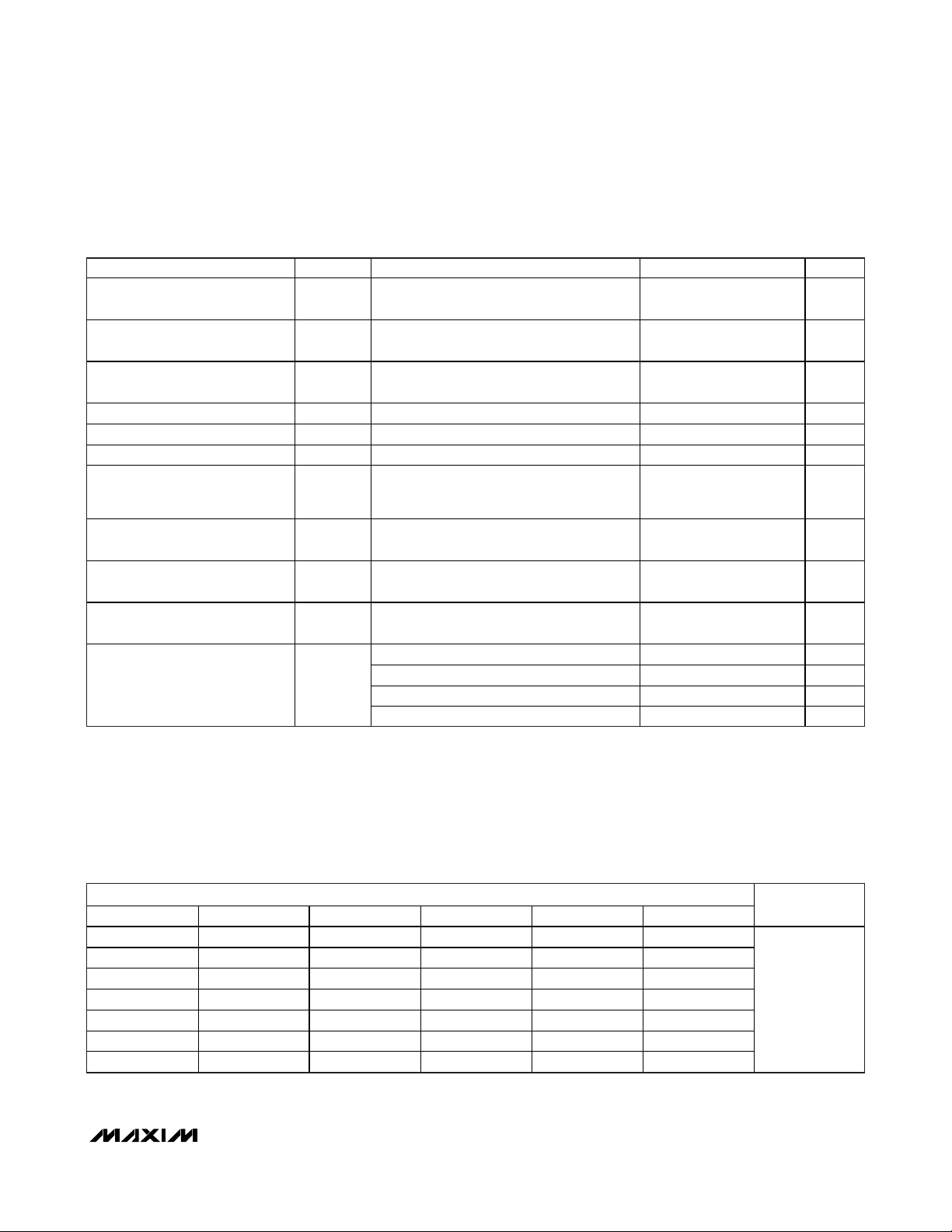
Typical Operating Characteristics
(TA = +25°C, unless otherwise noted.)
fC DEVIATION vs. TEMPERATURE
DS4625 toc01
TEMPERATURE (°C)
DEVIATION (ppm)
6040200-20
-40
-30
-20
-10
0
10
20
30
40
50
-50
-40
fC DEVIATION vs. V
CC
DS4625 toc02
VCC (V)
DEVIATION (ppm)
3.63.53.43.33.23.1
0.5
1.0
1.5
2.0
2.5
3.0
0
3.0
ICC vs. V
CC
DS4625 toc03
VCC (V)
CURRENT (mA)
3.53.43.33.23.1
60
70
80
90
100
110
120
130
140
50
3.0 3.6
I
CC_PU
I
CC_PL
ONE OUTPUT LOADED
Pin Description
PIN NAME FUNCTION
1 OE Active-High Output Enable. Has an internal pullup resistor (RPU).
2, 3 GND Ground
4 OP1 Positive Output 1 for LVPECL
5 ON1 Negat ive Output 1 for LVPECL
6 VCC Supply Voltage Input
A1, A2 N.C. No Internal Connection. Must be connected to ground.
A3 OP2 Positive Output 2 for LVPECL
A4 ON2 Negative Output 2 for LVPECL
— EP
Exposed Pad. The exposed pad must be used for thermal relief. This pad must be connected to
ground.
Page 5
DS4625
3.3V Dual-Output LVPECL Clock Oscillator
_______________________________________________________________________________________ 5
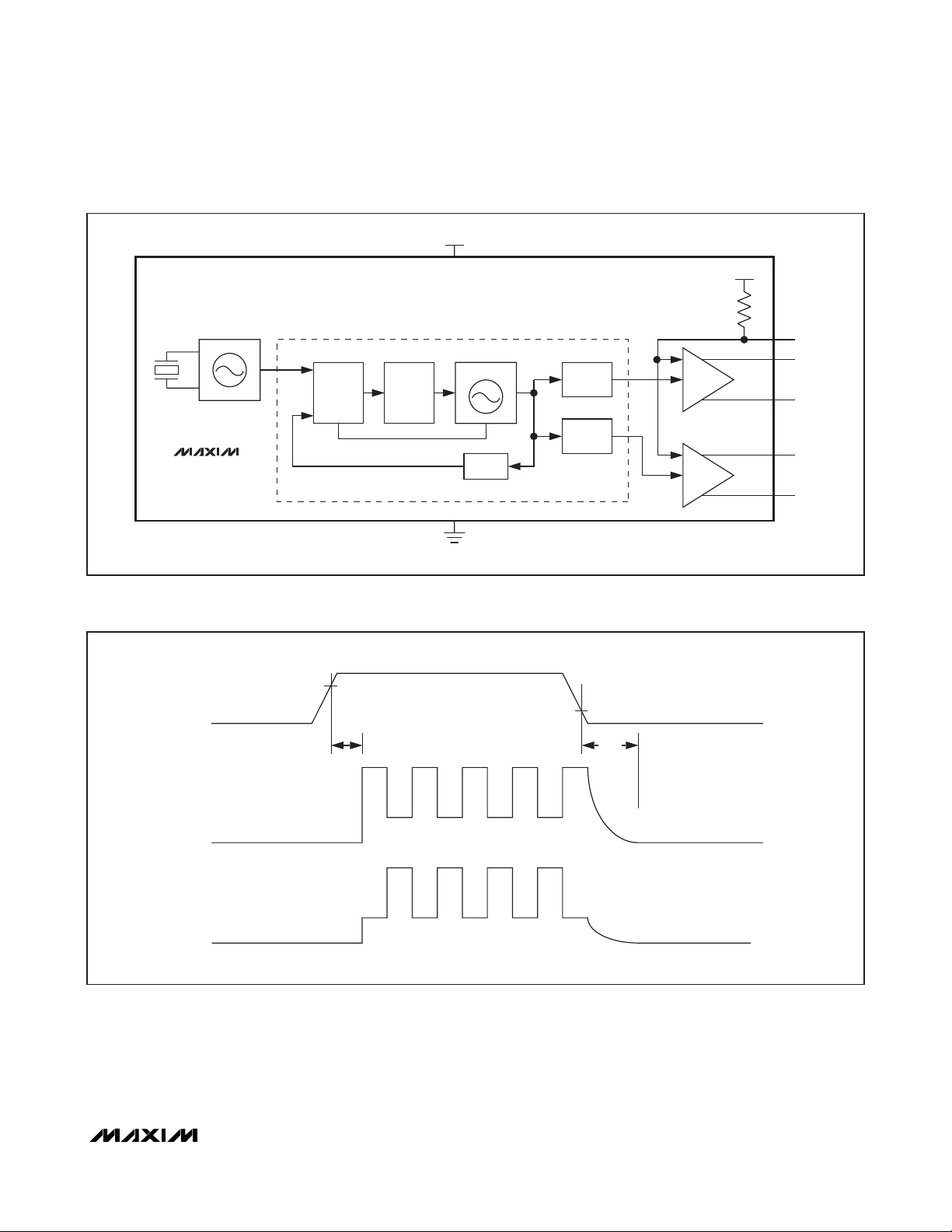
Figure 1. Block Diagram
Figure 2. LVPECL Output Timing Diagram When OE is Enabled and Disabled
X1
X0
X2
DS4625
PLL
PFD
LPF
V
GND
CC
LC-VCO
DIV P
DIV M
DIV N
LVPECL
LVPECL
V
CC
R
PU
OE
OP1
ON1
OP2
ON2
0.7 x V
OE
OP_
PECL_BIAS PECL_BIAS
ON_
PECL_BIAS
CC
t
PZA
0.3 x V
CC
t
PAZ
PECL_BIAS
Page 6

DS4625
3.3V Dual-Output LVPECL Clock Oscillator
6 _______________________________________________________________________________________
Detailed Description
The DS4625 is a dual-output, low-jitter clock oscillator
that produces frequency output pair combinations as
shown in the
Ordering Information/Selector Guide
table.
The phase relationship between the outputs is not guaranteed. The device combines an AT-cut, fundamentalmode crystal, an oscillator, and a low-noise PLL in a
5.0mm x 3.2mm surface-mount LCCC package.
The DS4625 provides dual LVPECL clock output drivers. The output drivers can be enabled and disabled
through the OE pin. The OE pin is an active-high CMOS
input that has an internal pullup resistor. When OE is
high, both output pairs are enabled.
Chip Information
PROCESS: Bipolar SiGe
Package Information
For the latest package outline information and land patterns,
go to www.maxim-ic.com/packages
. Note that a “+”, “#”, or
“-” in the package code indicates RoHS status only. Package
drawings may show a different suffix character, but the drawing
pertains to the package regardless of RoHS status.
Pin Configuration
PACKAGE TYPE PACKAGE CODE DOCUMENT NO.
10 LCCC L1053+H2
21-0389
Typical Application Circuit
TOP VIEW
*EXPOSED PAD
N.C. N.C.
+
A1 A2
1
OE
2
GND
GND
(5.00mm × 3.20mm × 1.49mm)
3
*EP
A3 A4
OP2 ON2
DS4625
6
5
4
V
ON1
OP1
CC
V
CC
0.1μF
0.01μF
DS4625
OE
GND
OP1
ON1
OP2
ON2
50Ω
50Ω
50Ω
50Ω
PECL_BIAS AT V
PECL_BIAS AT V
CC
CC
- 2.0V
- 2.0V
Page 7

DS4625
3.3V Dual-Output LVPECL Clock Oscillator
Maxim cannot assume responsibility for use of any circuitry other than circuitry entirely embodied in a Maxim product. No circuit patent licenses are
implied. Maxim reserves the right to change the circuitry and specifications without notice at any time.
Maxim Integrated Products, 120 San Gabriel Drive, Sunnyvale, CA 94086 408-737-7600 _____________________
7
© 2010 Maxim Integrated Products Maxim is a registered trademark of Maxim Integrated Products, Inc.
Revision History
REVISION
NUMBER
0 4/09 Initial release. —
1 3/10
REVISION
DATE
DESCRIPTION
Changed the operating temperature range limit from +70°C to +85°C, and added a new
part number to the Ordering Information table.
PAGES
CHANGED
1, 2, 3
 Loading...