

Page 1
General Description
The DS4303 is a nonvolatile (NV) sample and infinitehold adjustable voltage reference. The reference voltage is programmed in-circuit during factory calibration/
programming. Programming the reference voltage,
V
OUT
, is as simple as applying the desired voltage on
V
IN
and toggling the adjust pin (ADJ) to lock the V
OUT
voltage level indefinitely, even if the device is power
cycled. The DS4303 replaces current cumbersome factory adjustment arrangements with a low-cost solution
that can be adjusted using automated techniques. In
addition, the DS4303 has the ability to be readjusted
after the unit has been fully assembled and tested. This
results in a much more flexible manufacturing arrangement, lower inventory costs, and a quicker time-to-market.
Applications
Power-Supply Calibration
Threshold Setting
Offset Nulling
Bias Adjusting
Power Amps
Pressure Bridges
Factory-Calibrated Equipment
Features
♦ Precise Electronically Adjustable Voltage
Reference
♦ Enables Automated Factory Trimming of Devices
Needing Voltage Adjustment
♦ Can be Adjusted to Within ±1mV
♦ Wide Adjustable Output Voltage Range Within
300mV of the Supply Rails
♦ Low Temperature Coefficient
♦ ±1mA of Output-Current Drive
♦ NV Memory Stores the Voltage Indefinitely
♦ Output Short-Circuit Protection
♦ Low Cost
♦ Low Power Consumption
♦ 2.4V to 3.6V Single-Supply Operation
♦ Small 5-Lead SOT23 Package
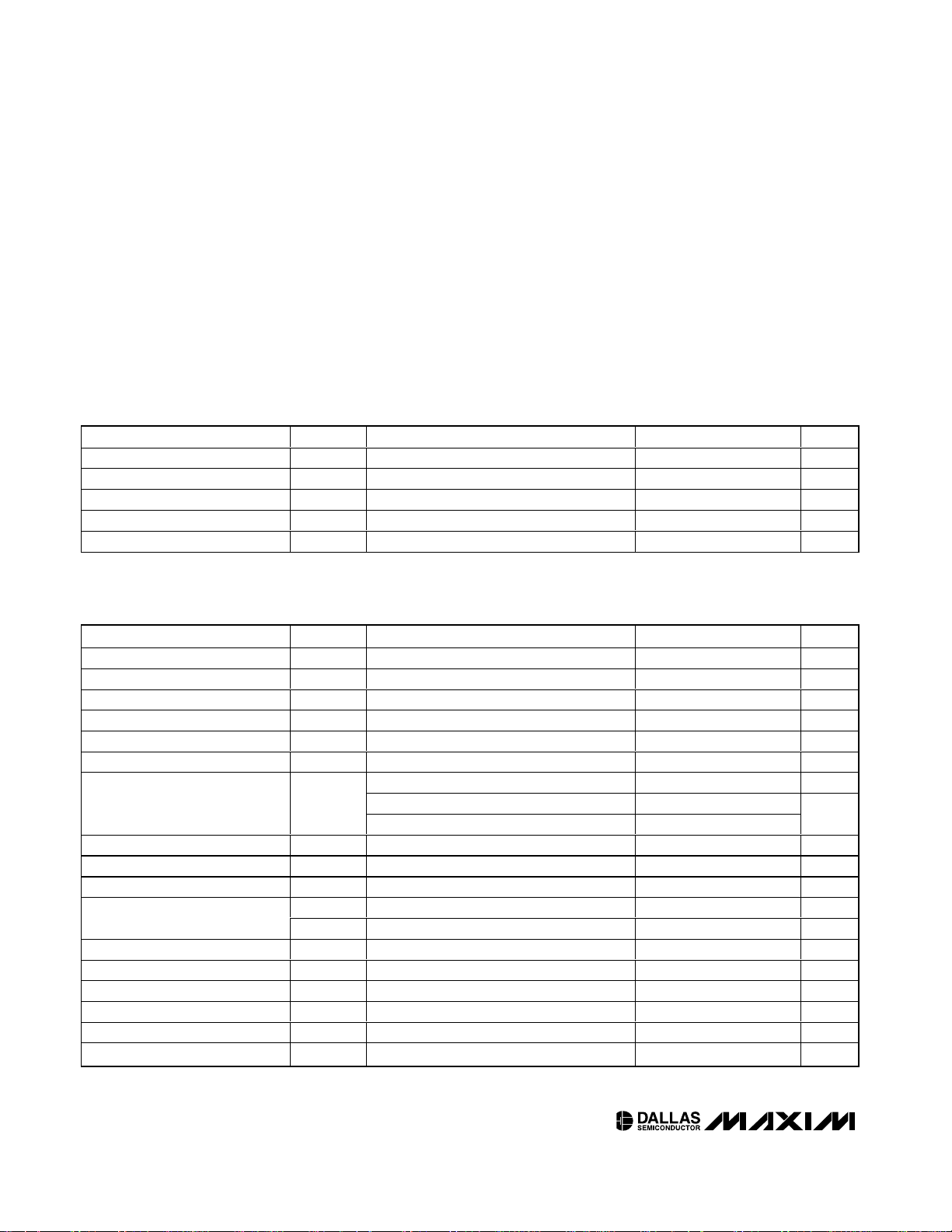
DS4303
Voltage Sample and Infinite Hold
______________________________________________ Maxim Integrated Products 1
GND
V
OUT
V
IN
15V
CC
ADJ
DS4303
SOT23
TOP VIEW
2
34
Pin Configuration
Ordering Information
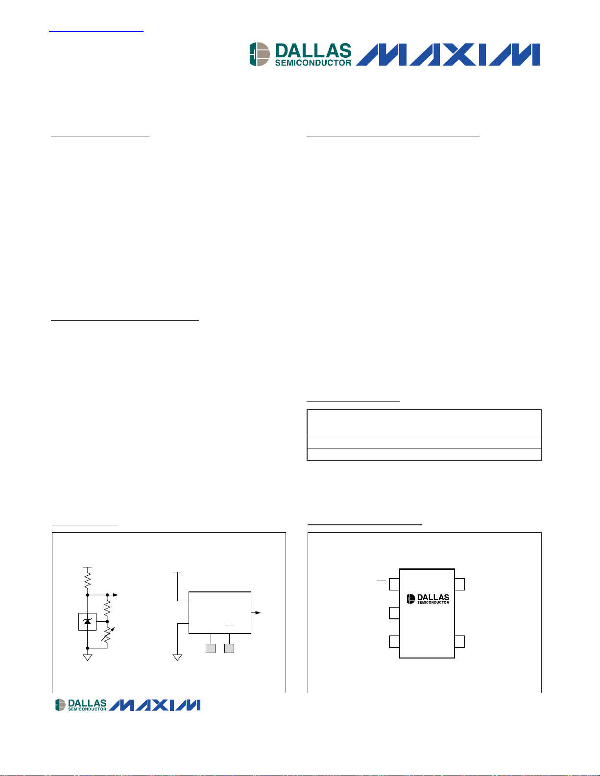
SHUNT
VOLTAGE
REFERENCE
ACCESS FOR
AUTOMATED
ALIGNMENT
REFERENCE
VOLTAGE
REFERENCE
VOLTAGE
HAND SELECTED
0.1% RESISTOR
OR MECHANICAL POT
EXISTING SOLUTION DS4303 SOLUTION
DS4303
V
CC
GND
V
OUT
VINADJ
V
CC
Typical Operating Circuit
Rev 0; 3/05
For pricing, delivery, and ordering information, please contact Maxim/Dallas Direct! at
1-888-629-4642, or visit Maxim’s website at www.maxim-ic.com.
PART
TEMP RANGE
PINPACKAGE
SOT
MARK
DS4303R/T&R
SOT23-5
4303
DS4303R+T&R
SOT23-5
4303+
+Denotes lead-free package.
查询DS4303供应商
-40°C to +85°C
-40°C to +85°C
Page 2
DS4303
Voltage Sample and Infinite Hold
2 _____________________________________________________________________
ABSOLUTE MAXIMUM RATINGS
RECOMMENDED OPERATING CONDITIONS
(TA= -40°C to +85°C)
Stresses beyond those listed under “Absolute Maximum Ratings” may cause permanent damage to the device. These are stress ratings only, and functional
operation of the device at these or any other conditions beyond those indicated in the operational sections of the specifications is not implied. Exposure to
absolute maximum rating conditions for extended periods may affect device reliability.
Voltage on VCCRelative to GND...........................-0.5V to +6.0V
Voltage on V
IN
, ADJ, and V
OUT
Relative to GND ...-0.5V to (VCC+ 0.5V), not to exceed +6.0V
Operating Temperature Range ...........................-40°C to +85°C
EEPROM Programming Adjust Temperature..........0°C to +70°C
V
OUT
to GND Short-Circuit Duration .........................Continuous
Storage Temperature Range .............................-55°C to +125°C
Soldering Temperature ...See IPC/JEDEC J-STD-020 Specification
PARAMETER
CONDITIONS
UNITS
Supply Voltage V
CC
(Note 1) 2.4 3.6 V
VIN Voltage Range V
IN
0.3
V
ADJ Logic 0 V
IL
V
V
OUT
Current V
OUTI
-1 +1 mA
V
OUT
Load V
OUTL
100 pF
ELECTRICAL CHARACTERISTICS
(VCC= +2.4 to +3.6V, TA= -40°C to +85°C, unless otherwise noted.)
PARAMETER
CONDITIONS
UNITS
Supply Current I
CC
VIN, ADJ and V
OUT
= open circuit 1.1 1.6 mA
VIN Resistance R
PD
95 kΩ
ADJ Pullup Resistance R
PU
18 kΩ
V
OUT
Voltage Range V
OUTR
(Note 1) 0.3
V
V
OUT
Tracking Accuracy
(Note 2) ±20 mV
V
OUT
Quantization V
OUTQ
(Note 3) ±1mV
-40°C to +85°C, V
OUT
= 0.4V
µV/°C
-40°C to +25°C, V
OUT
= 3.0V -5
V
OUT
Temperature Coefficient
+25°C to +85°C, V
OUT
= 3.0V -31 -13 +6
ppm/°C
V
OUT
Line Regulation
mV/V
V
OUT
Load Regulation
-1mA ≤ V
OUTI
≤ +1mA 5.5
mV/mA
Long-Term Stability
1000 hours at +25°C
ppm
e
n1
0.1Hz ≤ ƒ ≤ 10Hz 200
µV
P-P
V
OUT
Noise
e
n2
10Hz ≤ ƒ ≤ 1kHz 26
µV
RMS
V
OUT
PSRR
ƒ= 200kHz 21 dB
V
OUT
Self-Adjust Settling Time t
ST
(Note 4) 11 15
ms/V
EEPROM Programming Time t
W
(Note 5) 9 12 ms
Turn-On Time t
ON
VIN and ADJ = open circuit (Note 6) 10 µs
ADJ Toggle Low Time t
ADJ
100 ns
V
OUT
Factory Trimmed Value
+25°C, V
CC
= 3.3V (Note 7)
mV
SYMBOL
MIN TYP MAX
V
- 0.3
CC
-0.3 0.3 x V
CC
SYMBOL
V
OUTTA
MIN TYP MAX
V
- 0.3
C C
±104
V
OUTTC
V
OUTLN
V
OUTLD
V
OUTLTS
-4.0 +1.0
+28 +62
TBD
V
OUTPSRR
V
OUT FT
1200
Page 3
DS4303
Voltage Sample and Infinite Hold
_____________________________________________________________________ 3
ACTIVE SUPPLY CURRENT
vs. TEMPERATURE (V
OUT
= 0.3V)
DS4303 toc01
TEMPERATURE (°C)
SUPPLY CURRENT (mA)
603510-15
1.05
1.10
1.15
1.20
1.25
1.30
1.00
-40 85
VCC = 3.3V
VCC = 3.6V
VCC = 3.0V
VCC = 2.4V
IL = 0mA ADJ = V
CC
1.27
1.29
1.31
1.33
1.35
1.37
1.39
1.41
1.43
1.45
1.25
ACTIVE SUPPLY CURRENT
vs. TEMPERATURE (V
OUT
= 3.0V)
DS4303 toc02
TEMPERATURE (°C)
SUPPLY CURRENT (mA)
603510-15-40 85
VCC = 3.3V
VCC = 3.6V
IL = 0mA ADJ = V
CC
ACTIVE SUPPLY CURRENT
vs. SUPPLY VOLTAGE
DS4303 toc03
SUPPLY VOLTAGE (V)
SUPPLY CURRENT (mA)
3.43.22.6 2.8 3.0
1.05
1.10
1.15
1.20
1.25
1.30
1.35
1.40
1.00
2.4 3.6
TA = -40°C
TA = +25°C
TA = +85°C
IL = 0mA
Typical Operating Characteristics
(VCC= 3.3V, TA= +25°C, unless otherwise noted.)
Note 1: All voltages referenced to ground.
Note 2: Tracking accuracy is defined as V
OUT
- VINafter the DS4303 has completed self-adjustment.
Note 3: Quantization refers to the size of the voltage steps used to track the input signal.
Note 4: Settling time is the maximum amount of time V
OUT
requires to self-adjust. The settling time is determined by the following
formula: ∆V
OUT
x tST.
Note 5: EEPROM programming time is the hold time required after the DS4303 has completed self-adjustment before V
IN
or V
CC
can be removed or before ADJ can be toggled low once again.
Note 6: Turn-on time is defined as the time required for V
OUT
to reach its specified accuracy after the required supply voltage is
applied.
Note 7: V
OUT
not loaded.
Note 8: Guaranteed by design.
NONVOLATILE MEMORY CHARACTERISTICS
(VCC= +2.4V to 3.6V, unless otherwise noted.)
PARAMETER
CONDITIONS
UNITS
Programming Cycles +70°C (Note 8)
Cycles
SYMBOL
MIN TYP MAX
50,000
Page 4

DS4303
Voltage Sample and Infinite Hold
4 _____________________________________________________________________
Typical Operating Characteristics (continued)
(VCC= 3.3V, TA= +25°C, unless otherwise noted.)
3.553.503.35 3.40 3.453.30 3.60
-350
-300
-250
-200
-100
-150
-50
0
-400
LINE REGULATION
(V
OUT
= 3.0V)
DS4303 toc07
SUPPLY VOLTAGE (V)
OUTPUT VOLTAGE CHANGE (µV)
TA = -40°C
TA = +25°C
TA = +85°C
IL = 0mA
POWER-SUPPLY REJECTION RATIO
vs. FREQUENCY (V
CC
= 3.6V)
DS4303 toc08
FREQUENCY (kHz)
PSRR (dB)
100
25
30
35
40
45
50
20
10 1,000
V
OUT
= 0.3 V,
V
CC-AC
= 300mV
V
OUT
= 3.0 V,
V
CC-AC
= 300mV
RMS
DS4303 OUTPUT NOISE
(0.1Hz TO 10Hz)
DS4303 toc09
TIME (s)
V
OUT
(µV)
321
-200
-100
0
100
200
300
-300
04
VCC = 3.6V V
OUT
= 3.0V
DS4303 OUTPUT NOISE
(10Hz to 1kHz)
FREQUENCY (Hz)
µV
OUT NOISE
/ √
Hz
100
1
2
3
4
5
6
0
10 1000
DS4303 toc10
VCC = 3.6V V
OUT
= 3.0V
VOLTS
0.5
1.0
1.5
2.0
3.0
2.5
3.5
4.0
0
DS4303 TURN-ON
TRANSIENT
DS4303 toc11
1µs/div
V
CC
V
OUT
C
OUT
=100pF
DS4303 LOAD TRANSIENT
(V
OUT
= 3.3V, VCC = 3.6V)
DS4303 toc12
0.2ms/div
+1mA
-1mA
V
OUT
AC-COUPLED
200mV/div
I
OUT
-3
-2
-1
0
1
2
3
-4
LOAD REGULATION
(V
OUT
= 3.0V)
DS4303 toc05
LOAD CURRENT (mA)
OUTPUT VOLTAGE (mV)
0.50-0.5-1.0 1.0
VCC = 3.6V
TA = -40°C
TA = +25°C
TA = +85°C
LINE REGULATION
(V
OUT
= 0.3V)
DS4303 toc06
SUPPLY VOLTAGE (V)
OUTPUT VOLTAGE CHANGE (µV)
3.43.23.02.82.6
-2500
-2000
-1500
-1000
-500
0
-3000
2.4 3.6
TA = -40°C
TA = +25°C
TA = +85°C
IL = 0mA
LOAD REGULATION
(V
OUT
= 0.3V)
DS4303 toc04
LOAD CURRENT (mA)
OUTPUT VOLTAGE CHANGE (mV)
0.50-0.5
-4
-3
-2
-1
0
1
2
3
4
5
-5
-1.0 1.0
VCC = 3.0V
TA = -40°C
TA = +25°C
TA = +85°C
Page 5

DS4303
Voltage Sample and Infinite Hold
_____________________________________________________________________ 5
DS4303 LINE TRANSIENT
(V
OUT
= 2.0)
DS4303 toc13
0.2ms/div
3.6V
V
CC
3.0V
V
OUT
AC-COUPLED
200mV/div
DS4303 SHUTDOWN TRANSIENT
(V
OUT
= 3.3V)
DS4303 toc14
2ms/div
500mV/div
V
CC
V
OUT
C
OUT
= 100pF
DS4303 V
OUT
ADJUST TRANSIENT
(V
CC
= 3.6V, VIN = 3.3V)
DS4303 toc15
5ms/div
2V/div
1V/div
ADJ
V
OUT
DS4303 NORMALIZED V
OUT
vs. TEMPERATURE (V
OUT
= 0.4V)
DS4303 toc16
TEMPERATURE (°C)
V
OUT
(V/V)
603510-15
0.993
0.998
1.003
1.008
0.988
-40 85
VCC = 3.3V
0.9970
0.9975
0.9980
0.9985
0.9995
0.9990
1.0000
1.0005
0.9965
DS4303 NORMALIZED V
OUT
vs. TEMPERATURE (V
OUT
= 3.0V)
DS4303 toc17
TEMPERATURE (°C)
V
OUT
(V/V)
603510-15-40 85
VCC = 3.3V
Typical Operating Characteristics (continued)
(VCC= 3.3V, TA= +25°C, unless otherwise noted.)
Page 6

DS4303
Voltage Sample and Infinite Hold
6 _____________________________________________________________________
Detailed Description
The DS4303 provides a precise, NV output voltage,
V
OUT
, making it an ideal solution for factory calibration
of embedded systems. The DS4303 output voltage can
be adjusted over almost the entire operating supply
range of the device, and it can be precisely set to within ±1mV. A graphical description of the DS4303 is provided in the block diagram.
During factory calibration, a simple adjustment procedure must be followed. This entire procedure includes
setting VIN, toggling ADJ, waiting as V
OUT
self-adjusts,
and waiting for the completion of the EEPROM storage
cycle (See the timing diagram in Figure 1). At the start
of calibration, a voltage must be placed on VIN. This
voltage needs to be completely stable before the
adjustment procedure begins, and it must remain stable throughout the entire adjustment procedure. The
DS4303 will start its self-adjust procedure when the
ADJ pin is pulled low and held low for at least t
ADJ
,
after which it can be released at any time. Once ADJ
has been released, it should not be toggled again for
the remainder of the adjustment procedure. After the
falling edge on ADJ and the wait time, t
ADJ
, the V
OUT
self-adjust period begins. The length of the V
OUT
self-
adjust period can be determined using the formula
∆V x tST, where ∆V is | V
OUT OLD
- V
OUT NEW
|.
ADJ
GND
V
OUT
V
CC
V
CC
V
IN
V
CC
R
PD
R
PU
V
REF
ADC
AND
CONTROL
EEPROM
12-BIT
DAC
DS4303
Figure 1. Timing Diagram
PIN
FUNCTION
1 ADJ Adjust Control Input
2 GND Ground
3VINSample Voltage Input
4
Voltage Output
5VCCPower-Supply Voltage
Pin Description
Block Diagram
V
OUT
V
IN
ADJ
t
W
t
W
FIRST PROGRAMMING CYCLE ADDITIONAL PROGRAMMING CYCLES (IF REQUIRED)
t
ADJ
t
ADJ
t
ADJ
∆V
OUT
x t
ST
∆V
OUT
x t
ST
∆V
OUT
∆V
OUT
NAME
V
OUT
Page 7

DS4303
Voltage Sample and Infinite Hold
_____________________________________________________________________ 7
During the V
OUT
self-adjust period, the DS4303 inter-
nally adjusts the onboard DAC until V
OUT
matches VIN.
After V
OUT
has stabilized to within the tracking accura-
cy, V
OUTTA
, of VIN, it will be automatically stored in
EEPROM. The storage period lasts for the duration of
the EEPROM write time, tW. After the first adjustment
procedure has completed, V
OUT
can be measured,
and if necessary VINcan be readjusted and the entire
adjustment procedure can be repeated to fine-tune
V
OUT
within the V
OUTQ
range.
Following each self-adjust procedure, V
OUT
is saved
indefinitely, even if the DS4303 is power cycled.
Automated Programming Procedure
Figure 2 details an example of how the DS4303 can be
adjusted in an application. During factory alignment, a
three/four-node bed-of-nails is used to: (1) provide the
adjustment voltage through the VINpin, (2) control the
ADJ input, and (3) sense the needed feedback parameter. During manufacture, an automated test procedure adjusts V
OUT,
by changing VIN, until the feedback
parameter is optimized. After the bed-of-nails operation
is complete, both the VINand ADJ inputs are left open
circuit. V
OUT
can be readjusted at any time by following
the same procedure. The closed-loop nature of the
adjustment process removes all the system inaccuracies such as resistor tolerances, amplifier offsets, gain
mismatches, and even the inaccuracies in the automated equipment that provides the reference voltage.
Typical Operating Circuit
The typical operating circuit shows an example of how
the DS4303 can replace most existing calibration solutions. Many power supplies use a shunt voltage reference to provide the internal reference voltage, and
fine-tune adjustments are often made with hand-selected discrete resistors. The DS4303 replaces this cumbersome arrangement with a solution that is capable of
being adjusted by automated techniques. An additional
benefit of the DS4303 is the ability to provide a much
lower voltage (down to 300mV) than is possible with
shunt voltage references. Another benefit of the
DS4303 is the ability to be adjusted after the unit has
been fully assembled and tested, resulting in a much
more flexible manufacturing arrangement, lower inventory costs, and a quicker time-to-market.
Figure 2. Application Circuit
DS4303
2.4V TO 3.6V
EEPROM
GND
ADJ
V
IN
V
OUT
V
CC
VOLTAGE
SAMPLE AND
INFINITE
HOLD
DIGITALLY
CONTROLLED
VOLTAGE SOURCE
STEP 1:
SET REFERENCE
VOLTAGE
STEP 2:
TOGGLE ADJ
STEP 3:
DETERMINE IF
THE REFERENCE
VOLTAGE NEEDS
ADJUSTMENT
DIGITALLY
CONTROLLED
MEASUREMENT
DIGITAL PIN DRIVER
CIRCUITRY
REQUIRING
VOLTAGE
ADJUSTMENT
BED-OF-NAILS
TEST
ACCESS
PARAMETER MEASURED
DURING CALIBRATION
AUTOMATED TEST EQUIPMENT DEVICE UNDER TEST (DUT)
Page 8

DS4303
Voltage Sample and Infinite Hold
Maxim cannot assume responsibility for use of any circuitry other than circuitry entirely embodied in a Maxim product. No circuit patent licenses are
implied. Maxim reserves the right to change the circuitry and specifications without notice at any time.
8 _____________________Maxim Integrated Products, 120 San Gabriel Drive, Sunnyvale, CA 94086 408-737-7600
© 2005 Maxim Integrated Products Printed USA is a registered trademark of Maxim Integrated Products, Inc.
is a registered trademark of Dallas Semiconductor Corporation.
Layout Considerations
To prevent an inadvertent programming cycle from
occurring during power-up, minimize capacitive loading on the ADJ pin. A large capacitance on this pin
could potentially hold ADJ in a low state long enough
that a programming cycle is initiated.
Power-Supply Decoupling
To achieve best results, it is highly recommended that
a decoupling capacitor is used on the IC power-supply
pin. Typical values of decoupling capacitors are 0.01µF
or 0.1µF. Use a high-quality, ceramic, surface-mount
capacitor, and mount it as close as possible to the V
CC
and GND pins of the IC to minimize lead inductance.
Chip Topology
TRANSISTOR COUNT: 6001
SUBSTRATE CONNECTED TO GROUND
Package Information
For the latest package outline information, go to
www.maxim-ic.com/DallasPackInfo.
 Loading...